CJJ79XITS-7042MMDS BROADBAND BOOSTER
Axcera
Click to zoom
Application Details
- Equipment Class
- AMP - Amplifier
- Date of Grant
- Sep 17, 2000
- Application Purpose
- Original Equipment
- Date of Application
- Jul 17, 2000
- Equipment Note
- MMDS BROADBAND BOOSTER
- Frequency Range
- 2500.00000000 - 2690.00000000
- Company
- Axcera
- Country
- United States
Documents & Files
Document Text
Text extracted from the exhibit documents filed with the FCC. Open a document above to read the original.
Users Manual
ADC Telecommunications TECHNICAL MANUAL EXHIBIT II (PRELIMINARY) ITS-605C BROADBAND BOOSTER REV: 0 102 Rahway Road McMurray, PA 15317 USA Phone 412-941-1500 FAX 412-941-9421 ITS-605C BROADBAND BOOSTER TABLE OF CONTENTS I.INTRODUCTION: II.SYSTEM ITS-605C: A. SYSTEM DESCRIPTION B. SPECIFICATIONS C. INSTALLATION PROCEDURE IIIOPERATION ITS-605C: A. CONNECTIONS B. INITIAL TURN ON C. UNIT OPERATION D. INTERNAL LED INDICATORS E. MAINTENANCE IVBROADBAND BOOSTER AMPLIFIER SYSTEM: BLOCK DIAGRAM ........................................................................................................................... 1576-3000 INTERCONNECT .............................................................................................................................. 1576-8000 VBROADBAND BOOSTER TRAY: BLOCK DIAGRAM ........................................................................................................................... 1576-3100 INTERCONNECT .............................................................................................................................. 1576-8100 BROADBAND BOOSTER TRAY SUBASSEMBLIES ITS-605C SYSTEM DESCRIPTION The ITS-605C Boradband Booster is a wideband linear amplifier intended to be used as a booster in the MMDS/ITFS frequency bands, from 2500.00 to 2569.00 MHz, which allows the unit to operate with up to thirty one 6 MHz channels. The power capability of the unit varies with the number of channels according to specifications. The 605C is packaged in a weatherproof aluminum outdoor enclosure and uses an external convection cooled design. The 605C includes a preamplifier, power supply, and mounting hardware. . A multi-channel RF input signal enters the system at the broadband booster tray's RF input where it is filtered and amplified. The broadband booster tray also incorporates automatic level control to maintain the combined output power within the limits of the output amplifiers and all the necessary control logic of the system. SPECIFICATIONS: ITS-605C Broadband Booster Type of Emissions ........................................................................................ BOOSTER Frequency Range .............................................................................. 2500 to 2569 MHz DC voltage and total current of final amplifier stage .................. 10 volts DC at 5.48 amps (Class A - Not RF power dependent) Output Power Rating .............................................................. 1.5 watts (peak envelope) (250 mW total average) Performance Specifications Operating Frequency Range .............................................................. 2500 to 2569 MHz RF Output - Nominal: Impedance ............................................................................................... 50 Ω Connector ............................................................................................ Type N Power (average): 4 Channel ................................................................... 62.5 mW/channel 8 Channels ............................................................... 31.25 mW/channel 12 Channel ................................................................. 20.8 mW/channel 16 Channels ................................................................ 15.6 mW/channel 24 Channel ................................................................. 10.4 mW/channel 31 Channels .................................................................. 8.0 mW/channel Nominal Input Signal Range ........................................................ -83 to -53 dBm/channel Connector ........................................................................................... Type N Impeadance ............................................................................................. 50 Ω Out-of-Band Power .................................................................. Per FCC Rules (21.908) -25 dB max (at band edges): -40 dB max (250.00 KHz above and 250.00 KHz below band edges): -50 dB max (3.00 MHz above and 3.00 MHz below band edges): -60 dB max (20.00 MHz above and 20.00 MHz below band edges): Out-of-Band Power (Unoccupied Channel) ..... -25 dB max (at unoccupied channel edges) -40 dB max (250.0 KHz above and 250.0 KHz below occupied channel edges): -50 dB max (3.0 MHz above and 3.0 MHz below occupied channel edges): Harmonic Products ..................................................................................... -60 dB max Electrical Requirements Power Line Voltage ................................................................. 60VAC, ±10%, 50/60 Hz Power Consumption ....................................................................................... 260 Watts SPECIFICATIONS: ITS-605C Broadband Booster Environmental Maximum Altitude ......................................................................... 12,000 feet (3,660m) Ambient Temperature ................................................................................ -40 ° to 50 ° C Mechanical Dimensions: (WxDxH) Broadband Booster Tray .......... 18" x 21" x 11.5" (45.75cm x 53.33cm x 29.25cm) Weight: Broadband Booster Tray ......................................................... 60 lbs. (27.3 kgs) INSTALLATION PROCEDURE Unpacking Please inspect all material thoroughly upon arival. ADC certifies that upon leaving our facility the equipment was undamaged and in proper working order. The shipping container should be inspected for obvious damage indicative of rough handling. Remove the booster from the shipping container and inspect for damage. Check for dents, and scratches, or any broken connectors. Extract all packing material from inside and around the unit. Check for loose hardware and connectors, retighten if needed. Any claims against in-transit damage should be directed towards the carrier. Save all packing material in case unit must be returned. Installation of Booster The 605C is designed as a pole mount device, however, it may also be mounted on …
Text truncated - open the document above for the full version.
Users Manual
ADC Telecommunications TECHNICAL MANUAL EXHIBIT II (PRELIMINARY) ITS-605C BROADBAND BOOSTER REV: 0 102 Rahway Road McMurray, PA 15317 USA Phone 412-941-1500 FAX 412-941-9421 ITS-605C BROADBAND BOOSTER TABLE OF CONTENTS I.INTRODUCTION: II.SYSTEM ITS-605C: A. SYSTEM DESCRIPTION B. SPECIFICATIONS C. INSTALLATION PROCEDURE IIIOPERATION ITS-605C: A. CONNECTIONS B. INITIAL TURN ON C. UNIT OPERATION D. INTERNAL LED INDICATORS E. MAINTENANCE IVBROADBAND BOOSTER AMPLIFIER SYSTEM: BLOCK DIAGRAM ........................................................................................................................... 1576-3000 INTERCONNECT .............................................................................................................................. 1576-8000 VBROADBAND BOOSTER TRAY: BLOCK DIAGRAM ........................................................................................................................... 1576-3100 INTERCONNECT .............................................................................................................................. 1576-8100 BROADBAND BOOSTER TRAY SUBASSEMBLIES ITS-605C SYSTEM DESCRIPTION The ITS-605C Boradband Booster is a wideband linear amplifier intended to be used as a booster in the MMDS/ITFS frequency bands, from 2500.00 to 2569.00 MHz, which allows the unit to operate with up to thirty one 6 MHz channels. The power capability of the unit varies with the number of channels according to specifications. The 605C is packaged in a weatherproof aluminum outdoor enclosure and uses an external convection cooled design. The 605C includes a preamplifier, power supply, and mounting hardware. . A multi-channel RF input signal enters the system at the broadband booster tray's RF input where it is filtered and amplified. The broadband booster tray also incorporates automatic level control to maintain the combined output power within the limits of the output amplifiers and all the necessary control logic of the system. SPECIFICATIONS: ITS-605C Broadband Booster Type of Emissions ........................................................................................ BOOSTER Frequency Range .............................................................................. 2500 to 2569 MHz DC voltage and total current of final amplifier stage .................. 10 volts DC at 5.48 amps (Class A - Not RF power dependent) Output Power Rating .............................................................. 1.5 watts (peak envelope) (250 mW total average) Performance Specifications Operating Frequency Range .............................................................. 2500 to 2569 MHz RF Output - Nominal: Impedance ............................................................................................... 50 Ω Connector ............................................................................................ Type N Power (average): 4 Channel ................................................................... 62.5 mW/channel 8 Channels ............................................................... 31.25 mW/channel 12 Channel ................................................................. 20.8 mW/channel 16 Channels ................................................................ 15.6 mW/channel 24 Channel ................................................................. 10.4 mW/channel 31 Channels .................................................................. 8.0 mW/channel Nominal Input Signal Range ........................................................ -83 to -53 dBm/channel Connector ........................................................................................... Type N Impeadance ............................................................................................. 50 Ω Out-of-Band Power .................................................................. Per FCC Rules (21.908) -25 dB max (at band edges): -40 dB max (250.00 KHz above and 250.00 KHz below band edges): -50 dB max (3.00 MHz above and 3.00 MHz below band edges): -60 dB max (20.00 MHz above and 20.00 MHz below band edges): Out-of-Band Power (Unoccupied Channel) ..... -25 dB max (at unoccupied channel edges) -40 dB max (250.0 KHz above and 250.0 KHz below occupied channel edges): -50 dB max (3.0 MHz above and 3.0 MHz below occupied channel edges): Harmonic Products ..................................................................................... -60 dB max Electrical Requirements Power Line Voltage ................................................................. 60VAC, ±10%, 50/60 Hz Power Consumption ....................................................................................... 260 Watts SPECIFICATIONS: ITS-605C Broadband Booster Environmental Maximum Altitude ......................................................................... 12,000 feet (3,660m) Ambient Temperature ................................................................................ -40 ° to 50 ° C Mechanical Dimensions: (WxDxH) Broadband Booster Tray .......... 18" x 21" x 11.5" (45.75cm x 53.33cm x 29.25cm) Weight: Broadband Booster Tray ......................................................... 60 lbs. (27.3 kgs) INSTALLATION PROCEDURE Unpacking Please inspect all material thoroughly upon arival. ADC certifies that upon leaving our facility the equipment was undamaged and in proper working order. The shipping container should be inspected for obvious damage indicative of rough handling. Remove the booster from the shipping container and inspect for damage. Check for dents, and scratches, or any broken connectors. Extract all packing material from inside and around the unit. Check for loose hardware and connectors, retighten if needed. Any claims against in-transit damage should be directed towards the carrier. Save all packing material in case unit must be returned. Installation of Booster The 605C is designed as a pole mount device, however, it may also be mounted on …
Text truncated - open the document above for the full version.
External Photos
Note: The followng Internal Photos were taken from Section 4.3 of the Report. 4.3.1Front view, 605C Broadband Booster (Closed Door) 4.3.3Rear view, 605C Broadband Booster 4.3.4Bottom view, 605C Broad band Booster 4.3.5Top view, External Power Supply (Closed Door) 4.3.6Top view, External Power Supply (Open Door) 4.3.7Top view, +15 dB Preamplifier 4.3.8Top view, +25 dB Preamplifier
External Photos
4.3.4 Bottom view, Broadband Booster Manufacturer Identification/FCC Identification Label
ID Label/Location Info
Note: The following label location drawing was taken from section 4.0 of the Report. 4.0IDENTIFICATION LABELS/LABEL PLACEMENT AND PHOTOGRAPHS 4.2 Rear Panel Drawing (Label Placement):
Internal Photos
Note: The following Internal Photo was taken from Section 4.3 of the Report. 4.3.2Front view, 605C Broadband Booster (Open Door)
Operational Description
2.0TECHNICAL DESCRIPTION 2.4Circuit Description General The 605C Broadband Booster is comprised of a remote preamplifier, booster amplifier and external power supply. The preamplifier may be chosen with a gain of 15 or 25 dB and is mounted in an outdoor enclosure suitable for mounting near the receive antenna. The preamplifier output is normally connected through low loss coaxial cable to the input of the booster. The booster includes automatic level control, power amplification stages, DC/DC power converter, and control circuitry. The combined peak envelope output power of the tray is used to develop the automatic level control voltage. The booster unit receives power through a coaxial connector from an external power supply module. The external power supply is supplied with standard 117V/220 VAC power. Preamplifier The amplifier stages of the preamplifier are wideband gallium arsenide transistor amplifier stages. The input stage uses low noise devices to maintain a low system noise figure. The second stage uses higher power transistors to insure a wide dynamic range. Both stages are wideband microstrip designs with class A bias and no operation adjustments. Booster Amplifier The amplified signal from the preamp enters the booster at J6 on the bottom of the unit and is applied to a circulator then fed to the Broadband Bandpass Filter (2140-1004) which provides the initial selectivity to the system. The output of the filter is fed to a second circulator and then to the input (J1) of the Two Stage Amplifier Module (11576- 1126). This module consist of two cascaded GaAs FET amplifiers (ATF10136 driving a FLL 101ME) with an overall gain of approximately 27 dB. The output of the Two Stage Amplifier Module is fed to the PIN Diode Attenuator Module (1575-1135) which uses a series configuration Pin Diode attenuator circuit. The gain of the attenuator is controlled using a peak detected sample of the output amplifier. By controlling the gain of this attenuator, the output power can be regulated, maintaining a constant output regardless of minor changes in the input signal. The Output signal from the PIN Diode Attenuator is fed to the Single Stage Amplifier Module which consist of a single GaAs FET (ATF10136) amplifier stage with a gain of approximately 13 dB. The output of this module is applied to a circulator then to the Three Stage Amplifier Module (1516-1107) which consist of three cascaded GaAS FET amplifiers (FLL101ME driving a FLL351ME driving a FLL120 MK) with an overall gain of approximately 37 dB. The output of the Three Stage Amplifier Module is applied to a circulator then fed to the input of a Broadband Filter (2140-1033) then to the input of the Single Stage 10W Amplifier Module (1576-1117 or 1576-1118) which consist of a single GaAs FET amplifier (FLL200IB-3) with a gain of approximately 11 dB. The output of the module (J2) is applied to a circulator then to the RF output jack (J2) on the bottom of the unit. An internal 20 dB microstrip coupler is used to obtain a sample of the RF output. This RF sample connects to the Average Power Detector/Buffer Board (1517- 1104). 2.0TECHNICAL DESCRIPTION 2.4Circuit Description - continued The signal enters the Average Detector/Buffer Board at J1 and is applied to a Wilkinson Coupler which splits the signal. One output of the splitter is amplified and fed to the RF sample output jack (J4) of the module, which connects to the RF sample jack (J5) on the bottom of the unit. The other output of the coupler is applied to an average detector circuit that generates an ALC voltage, which is used to control the PIN Diode Attenuator. The Booster Control Board (1576-1101), provides the capability to control and monitor the operating status of the booster. The board is designed to protect the booster in the event of one of the following faults: over temperature, loss or reduction in output power, loss of input signal and loss of the -5 VDC GaAs FET bias voltage. The Booster Control Board also provides the capability to remotely control and monitor the booster status via the Remote Diagnostics (J8) and External Control (J7) jacks located on the bottom of the unit. The DC biasing of the FET amplifiers within the various modules is controlled and filtered by daughter boards, which are soldered directly to the main boards. The DC bias drain to source currents are set by adjusting the negative gate to source voltages which are adjusted by potentiometers on the daughter boards. The 605C booster is powered by an external 60VAC source. The AC source enters the booster at J3 and is applied to the Input Protection Board (1517-1102) which provides over voltage and over current protection using a 3A inline fuse and MOV varistor. The output of the Input Protection Board is connected to a Toroid transformer. The Toroid transformer provides two 20 VAC secondary windings. The first winding is sent to a full wave bridge rectifier, which supplies a positive 48 VDC to the DC/DC Converter Board (1517-1111). The second winding is supplied to a full wave bridge rectifier circuit located on the ±12V -5V DC Power Supply Board (1576-1102) then to negative 5 volt and negative 12 volt voltage regulators. The DC/DC Converter Board contains a DC/DC converter IC and the required support circuitry to produce a constant regulated 10VDC output signal that is used to supply the FET amplifiers in the Three Stage Amplifier Module and the Single Stage 10W Amplifier Module via the Two Section Bias Protection Board (1576-1102). An Inhibit input from the Booster Control Board drives a magnetic latching relay, which in tun drives the on/off (enable) input of the DC/DC converter IC. This input is used to shut off the converter IC and remove power from the output amplifiers in the event of an input signal loss. The Bias Protection Board distributes the -5V gate bias and + 10V drain bias to the Three Stage Amplifier and Single Stage Amplifier Modules. The -5V line from the -5V/±12 Power Supply Boar…
Text truncated - open the document above for the full version.
Parts List/Tune Up Info
2.0TECHNICAL DESCRIPTION 2.5Alignment Procedure In the following procedure, the complete Multi-Channel Boaster is adjusted for optimum performance. This alignment procedure is performed by adjusting each circuit for its specified performance while observing the appropriate output parameters of the board or subassembly being adjusted. Because of the broadband nature of the amplifier stages, this is a straightforward procedure, easily accomplished is RF test equipment is available. In this procedure, the input signals are first connected and each circuit is adjusted in sequence by connecting the test equipment to the specified point. Equipment required: 1. Spectrum Analyzer (with tracking generator) 2. Network Analyzer 3. Power Meter 4. Multi-channel test signal 5. 30 dB Coupler 6. Attenuators 7. Digital Multimeter (DMM) 1. Connect power to the booster. Terminate the output with a 50W 50Ω load. 2. Set the network analyzer for the following settings: Start Frequencybeginning of range Stop Frequencyend of range Power Level-45 dB (in combination with attenuators and power level) Reference Level0 dB 3. Set S2 on Booster Control board for manual. 4. Calibrate cables from network analyzer for transmission. 5. Connect the RF out cable to J1 RF I/P and the RF In cable to J2 of the Broadband Bandpass Filter. Tune the filter, and verify that it is within specifications. 6. Reconnect rigid to J2 of the filter, and move RF In cable of the analyzer to J2 of the A10 Two Stage Amplifier. Tune the module for gain and output power specifications. 2.0TECHNICAL DESCRIPTION 2.5Alignment Procedure - continued 7. Reconnect J2 to Two Stage Amplifier and move RF In cable of the analyzer to J2 of the PIN Attenuator Module. Turn ALC PIN Attenuator Bias voltage to maximum using R56 on the Booster Control board and measure gain. ALC PIN Attenuator bias voltage should be > 11.5V at FL2 of the module. There should be 4 dB of loss through this module. Reset voltage to 4.0V at FL2 of the PIN Attenuator Module. Response should be within ±0.5 dB. Reconnect J2 to PIN Attenuator Module. 8. Calibrate cables from network analyzer for Ch. 1 for Transmission, and Ch. 2 for Reflection. Connect RF Out cable to J1 of A14 Single Stage Amplifier Module. Connect RF In cable to J2 of module. Tune the module for gain, reflected, and output power specifications. Reconnect rigid to J1 and J2 of the module. 9. Move RF Out cable from the analyzer to J1 of the circulator (A15) and the RF In cable from the analyzer to J2 of the Three Stage Amplifier Module. Tune the Module for gain and output power specifications. Reconnect the rigid to J1 of the circulator and J2 of the amplifier module. 10. Move RF Out In cable from J2 of the Three Stage Amplifier Module to the RF output (J2) of the booster. Tune the Single Stage Amplifier Module (A18) for gain and output power specifications. Reconnect rigid to J1 of the circulator and J2 of the amplifier module. 11. Verify that the voltage at FL2 of the Single Stage Amplifier Module is 10.2V. 12. Connect 45 dB of attenuation on the RF Out port of the network analyzer. Calibrate the cables from the network analyzer to transmission. 13.Connect the calibrated cables as shown in the figure below. 14. Turn PIN Attenuator bias voltage to maximum at FL2 of the PIN Attenuator Module. Measure the open loop gain of the booster. (Note: compensate for the 30 dB coupler). Verify that the open loop gain is within specifications. Reset PIN Attenuator voltage for 4.0V at FL2 of the module. 15. Measure response across the frequency band. Response should be within ±1 dB. 2.0TECHNICAL DESCRIPTION 2.5Alignment Procedure - continued 16.Connect the booster as shown below: 17. Record the Peak Power/Ch and the average power with two input carriers. 18. Measure and record the Composite Triple Beat for the booster. Verify CTB meets specifications. 19. Set spectrum analyzer for the following settings: Span10MHz Res BW300KHz Sweep500msec Atten0 dB ReferenceTop line of analyzer 20. With one carrier present, set delta marker on carrier peak and disconnect the RF I/P to the booster. Subtract 13 from the absolute value of the difference in level. This is the Carrier to noise level. Verify the level is within specifications. 21. Apply two carriers (MDS1 and MDS2) to the input of the booster. 22. Set voltage on J8 (center pin) on Booster Control Board to 0.2V using R13 on the Average Power Detector board. 23. Switch S2 to ALC, set R42 on Booster Control board for 29 dBm. 24. Decrease input level in 1 dB increments until the output power drops 1 dB. Adjust R57 on the Booster Control board until Low Output LED (DS4) lights. 25. Verify that the Low Output LED turns off when the input level is increased 1 dB. 26. Increase input level until the output level is 0.3 dB higher than the original output power level.. Adjust R55 on the Booster Control board until the Overdrive LED (DS3) lights. 27. Verify that the Overdrive LED turns off when the input level is decreased by 1 dB. 28. Verify that there is a 30 dB ALC range for the booster. 2.0TECHNICAL DESCRIPTION 2.5Alignment Procedure--continued 29. Adjust the input signal to the proper level. 30. Set S2 switch on the Booster Control board to manual. 31. Calibrate and connect network analyzer as in step 2, 4, and 5. 32. Plot the response of the booster and verify the flatness is within specifications.
Schematics
9 9 8 8 7 7 6 6 5 5 4 4 3 3 2 2 1 1 EE DD CC BB AA +12V -5V -Vg -Vg+5.1V+10V NOTES: 1. ALL RESISTORS ARE 1/8W, 5% UNLESS NOTED. 2. ALL CAPACITANCE VALUES ARE IN uF,ALL RESISTANCE VALUES ARE IN ohms, UNLESS OTHERWISE NOTED. B 03/06/97 CAS 1576-3124 0 11 ------- ------- --- SCH., 2 STAGE BIAS DAUGHTER BOARD BKW BKW 4/7/97 4/7/97 ITS CORPORATION REVECNDATEAPV TITLE THIS PRINT IS THE PROPERTY OF ITS CORP IT SHALL NOT BE COPIED WITHOUT PERMISSION MATERIAL FINISH DWN CHK RELSCALESHEET REV REV ECN DAT E APV DWG. NO. OF R100 51 C101 .001 + C100 4.7 10V L100 FERRITE BEAD R101 51 C103 .001 + C102 4.7 10V L101 FERRITE BEAD R109 47 R108 47 R118 200 CW 3 2 1 R119 27 C108 .001 R102 51 C105 .001 + C104 4.7 10V L102 FERRITE BEAD R103 51 C107 .001 L103 FERRITE BEAD R111 47 R110 47 R116 200 CW 3 2 1 R117 27 C109 .001 CR100 10V 1N4740 CR101 10V 1N4740 R112 10 1W K1 1 2 6 7 14 8 913 R114 47 R113 47 C112 .1 + C113 10 35V C110 .1 + C111 10 35V L105 .47uH FL1 FL2 L104 .47uH A1A2A3A4 CR102 5.1V 1N4733A + C106 10 35V E1 R115 100/1W A A B B C C D D E E F F G G H H I I 55 44 33 22 11 SMA +12V I/P SMA ALC BIAS VOLT I/P 1 9013 8/1 4/97 BK W FL1 WAS FL2, FL2 WAS FL1. (TMY) DEL. PART# ON THEHY BRID COUPLERS. JKF A0 20002462 4/28/9 9 BK W 1576-3134 A0 SCH, PIN ATTEN. BD. 2 - 3 GHZ (1576-1134) JKF 4/8/97 B1 OF 1 BKW4/8/97 4/8/97 BKW ADC Telecommunications REV ECO DATEAPV TITLE THIS PRINT IS THE PROPERTY OF ADC, IT SHALL NOT BE COPIED WITHOUT PERMISSION MATERIAL FINISH DWN CHK REL SCALESHEET REV REV ECO DATE APV DWG. NO. --- ----- ----- +12V +12V +12V J1 E1 R7 100 R8 100 C1 100pF FL1 + C13 10 35V C15 100pF C16 15pF C6 100pF R3 1K R5 1K R6 1K R4 1K C3 15pF C4 .01 C5 100pF CR1 HSMP4810 CR2 HSMP4810 CR3 HSMP4810 CR4 HSMP4810 CR5 HSMP4810 CR6 HSMP4810 CR7 HSMP4810 CR8 HSMP4810 L4 .47uH L1 .47uH L3 .47uH C7 100pF C2 100pF R2 100 R1 100 J2 L2 .47uH C11 100pF C14 .1 C8 15pF L5 .47uH Q1 2N4124 1 2 3 B E C C9 .01 C10 .01 C17 .01 CR10 1N914 R10 220 R11 1.2K R9 1.2K CR9 1N914 C12 .1 FL2 HC1 12 34 HC2 12 34 NOTE: 1) ALL RESISTORS ARE 1/8W UNLESS OTHERWISE NOTED. 2) ALL CAPACITORS ARE IN uF UNLESS OTHERWISE NOTED. 3) ALL INDUCTORS ARE IN uH UNLESS OTHERWISE NOTED.
Test Report
EXHIBIT I FCC TYPE ACCEPTANCE REPORT ADC TELECOMMUNICATIONS MODEL ITS-605C FCC ID-CJJ79XITS-7042 BROAD BAND BOOSTER Date Filed July 18, 2000 This application is filed in compliance with Part 2, Part 21 and Part 74 of the FCC Rules and Regulations. ADC Telecommunications 102 Rahway Road McMurray, PA 15317 Rev. 1.0 TABLE OF CONTENTS 1.0 IDENTIFICATION OF APPLICANT AND EQUIPMENT 1.1 Applicant 1.2 Equipment Model Number 1.3 Manufacturing Plans 2.0 TECHNICAL DESCRIPTION 2.1 Introduction 2.2 Technical Specifications 2.3 Performance Specifications 2.4 Circuit Description 2.5 Alignment Procedure 2.6 Block Diagrams 3.0 ENGINEERING DATA 3.1 RF Power Measurement 3.2 Occupied Bandwidth 3.3 Out-of-Band Power 3.4 Unoccupied Channel Emissions 3.5 Radiated Emissions 3.6 Frequency Stability 3.7 Test Equipment 4.0 IDENTIFICATION LABLES/LABEL PLACEMENT AND PHOTOGRAPHS 5.0 CERTIFICATION OF TEST DATA 1.0IDENTIFICATION OF APPLICANT AND EQUIPMENT 1.1Applicant: ADC Telecommunications 102 Rahway Road McMurray, PA 15317 The above name and address is printed on a label attached to the rear panel of the equipment. 1.2Equipment and Model Number: ITS-605C This information is provided on the front panel of the equipment. 1.3ADC Telecommunications shall manufacture this product in quantities necessary to satisfy market demand. 2.0TECHNICAL DESCRIPTION - MODEL ITS-605C 2.1Introduction The ITS-605C is a wideband linear amplifier intended to be used as a digital multi-channel booster in the MMDS/ITFS frequency band (2500.00 to 2690.00 MHz). The power per channel capability of the unit varies with the number of channels according to specifications. The 605C is packaged in a weatherproof aluminum outdoor enclosure and uses an external convection cooled design. Functionally, the unit is comprised of a broadband booster, a +15 dB or +25 dB preamplifier and an external power supply. The RF input signal enters the system at the RF input of the pre-amplifier then is fed to the broadband booster tray's RF input where it is filtered and amplified. The broadband booster tray also incorporates automatic level control to maintain the combined output power within the limits of the output amplifiers and control circuitry to disable the broadband amplifier when no input signal is present. The 605C utilizes GaAS FET amplifier modules for amplification of the RF signal. The unit is supplied complete with mounting hardware. Parameters and specification for operation of this unit are provided on the following pages, and a complete circuit description and alignment procedure are also included in this report. Refer to the overall system block diagram and the particular referenced schematics in the attached circuit description section of this report. 2.0TECHNICAL DESCRIPTION 2.2Technical Specifications Type of Emissions .................................................................................................... BOOSTER Frequency Range ................................................................................................... 2500 to 2690 DC voltage and total current of final amplifier stage ...................... 10 volts DC at 5.48 amps (Broadband Amplifier tray) (Class A - Not RF power dependent) Operating Frequency Range ................................................................................. 2500 to 2690 Total Output Power Capability ........................................................ 1.5 Watts (peak envelope) (250 mWatts total average max) RF output (average): 4 Channels ....................................................................................... 62.5 mW/Channel 8 Channel ............................................…
Text truncated - open the document above for the full version.
Contact Information
Applicant
Kenneth Foutz(Sr. Vice President)
Technical Specifications
| # | Rule Parts | Frequency Range | Power Output | Emission | Tolerance |
|---|---|---|---|---|---|
| 1 | 21,74 | 2.50 GHz - 2.69 GHz | 250.00 mW | BOOSTER | Hz |
Other Applications from Axcera

CJJ79XITS-7045
Dec 02, 2001Model: BTS-7010 Multi-Channel MMDS/ITFS Booster
Equipment Class
AMP - Amplifier
CJJ79XITS-7041
Jun 28, 2000MMDS/ITFS TRANSLATOR
Equipment Class
TBC - Licensed Broadcast Station Transmitter
CJJ79XITS-7040
Apr 24, 2000MDS/MMDS/ITFS Digital Transmitter
Equipment Class
TBC - Licensed Broadcast Station Transmitter
CJJ79XITS-7037
Apr 02, 2000ITFS/MMDS Broadband Translator
Equipment Class
AMP - Amplifier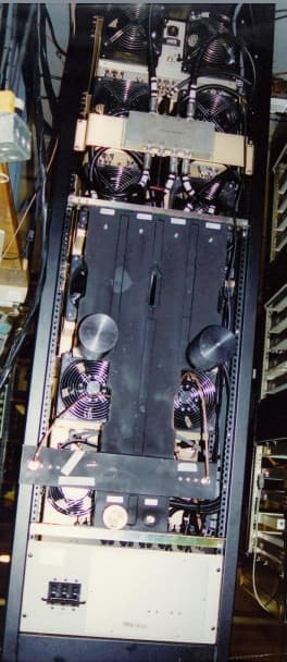
CJJ79XITS-7036
Mar 29, 2000MMDS/ITFS BROADBAND TRANSLATOR
Equipment Class
AMP - Amplifier