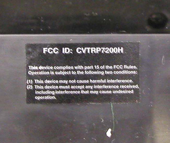
CVTRP7200HRadio Controlled Toy (Receiver)
Nikko Co Ltd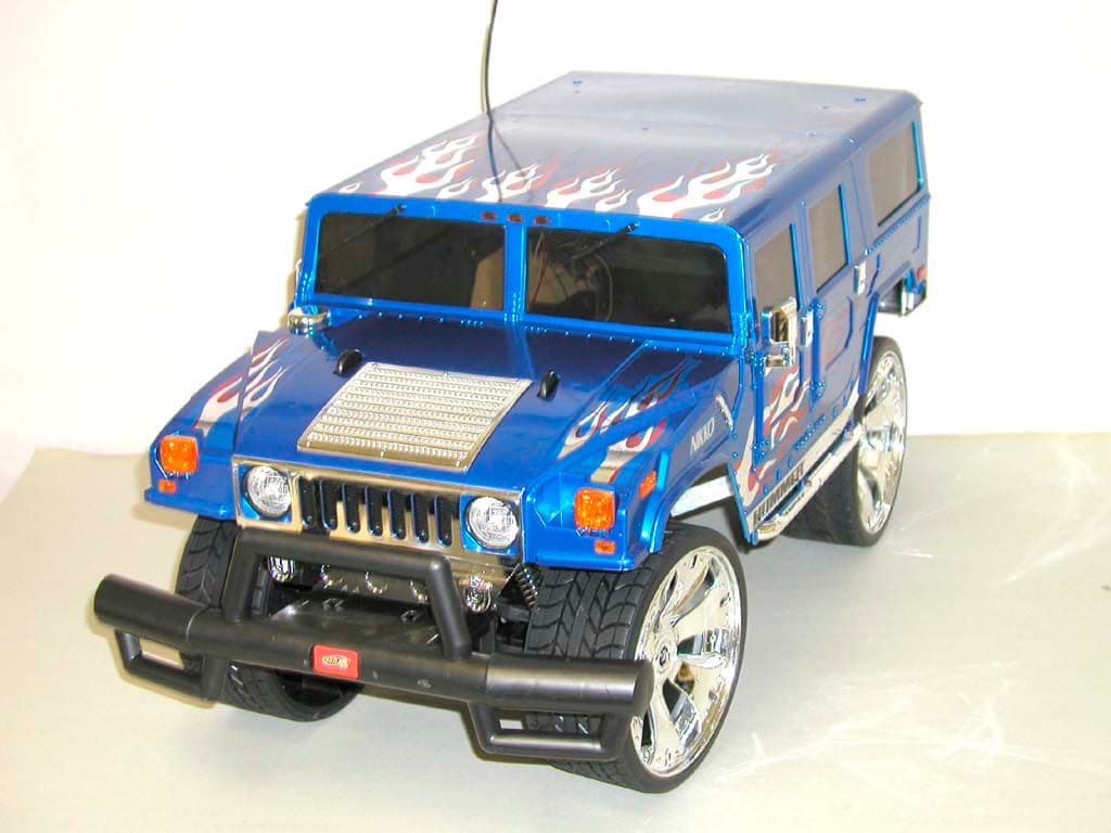
Click to zoom
Application Details
- Equipment Class
- CRR - Superregenerative Receiver
- Date of Grant
- Jul 14, 2005
- Application Purpose
- Original Equipment
- Date of Application
- Jul 14, 2005
- Equipment Note
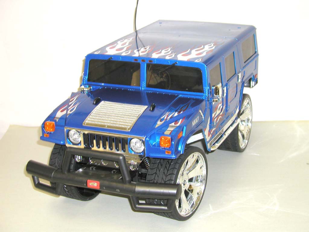
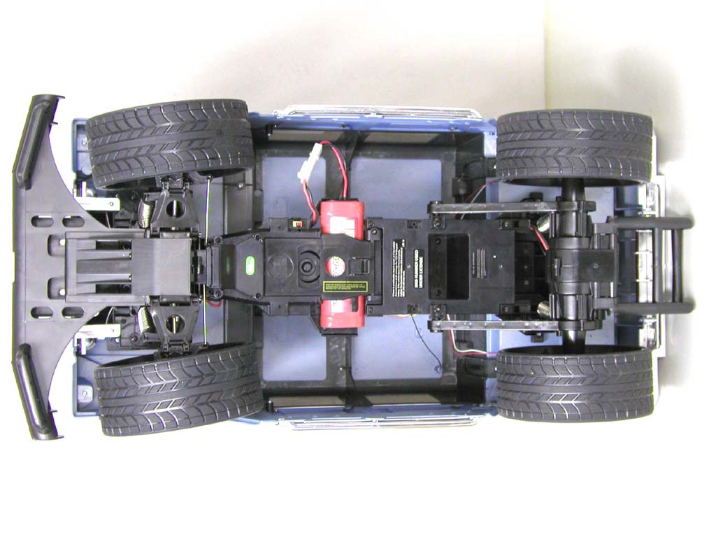
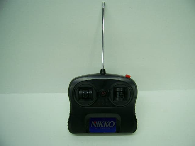
- Radio Controlled Toy (Receiver)
- Frequency Range
- 49.83000000 - 49.89000000
- Company
- Nikko Co Ltd
- Country
- Japan
Documents & Files
Document Text
Text extracted from the exhibit documents filed with the FCC. Open a document above to read the original.
Users Manual
KMNA-060009 NM0-010605 Do not charge Battery Pack immediately after use. Wait until it has cooled before charging. Avoid short circuits. Short circuits will cause overheating, burning of the cords and other damages to the battery Pack and Charger. The Ni-Cd Battery Charger should be used for charging one Battery Pack. Do not use the Charger for charging other type of batteries and battery packs Do not use the Charger as a direct current outlet for other electrical appliances or machines. Make sure that the Battery Pack and Charger are kept out of the hands of infants and small children while charging. Do not charge near fires, where the temperature is extremely high, or where it is wet or damp. The charger will become slightly heated while charging. Allow sufficient free space around the Charger. If the power of the battery pack is weak in spite of proper charging, the batteries may be worn out from repeated use. Replace it with a new Ni-Cd battery pack. Dispose of use Ni-Cd battery packs correctly. Disconnect the supply before making or breaking connections to the battery. Only use batteries or accumulators of the recommended type or a similar type. WARNING AGAINST RECHARGING NON-RECHARGEABLE BATTERIES. Please use this battery charger only for the charge of the rechargeable battery pack. The Ni-Cd battery pack should be charged under the supervision of an adult. CAUTION Charger Household outlet Ni-Cd battery pack Press Charger’s connector Battery’s Connector RECHARGING "WARNING! USE UNDER THE DIRECT SUPERVISION OF AN ADULT." The newly purchased Ni-Cd pack is not charged. Charge before operating. 1. Join the connector of the charger to the connector of the Ni-Cd battery pack. 2. Plug the charger into an electrical outlet. 3. Recharge for about 4-5 hours. 4. When the recharging is over, plug out the charger from the electrical outlet and detach the connectors. When playing for the first time after purchase, or after a long interval, the battery power may be weak. Even after recharging, the playing time can be relatively short. The battery will gradually regain power after 2 or 3 repetitions of usage and recharging. BOTTOM VIEW VEHICLE TOP VIEW 2 Pass the antenna wire through the antenna tube, then insert the tube into the antenna tube holder. If the antenna tube cannot be successfully inserted into the antenna tube holder, try holding the root of the antenna wire with fingers of one hand and extending the wire with fingers of the other hand. 1. ATTACHING ANTENNA TUBE * Note: Be careful not to pull antenna wire too strong. PREPARATION FOR STARTING OPERATION 2. INSTALLING TRANSMITTER ANTENNA Place the transmitter antenna into the antenna holder to screw it in clock-wise. Do not extend the antenna when installing. It’s dangerous. If the antenna is not screwed in securely, the vehicle may move erratically. Screw the antenna securely. Transmitter antenna 3. INSTALLING THE BATTERIES TRANSMITTER To remove the battery lid, press the point marked “OPEN” and pull the lid downward. Install battery make sure that (+) and (-) poles are positioned properly. * Dispose the used batteries separately from other trash. One 9 volt (006P) battery Antenna wire Antenna tube Antenna tube holder 3 4 ON OFF (1) USING THE CONTROLLER (5) Turn “OFF” the vehicle. Steering control stick Forward / Reverse control stick Red LED power indicator LEFT / STRAIGHT / RIGHT FORWARD STOP (NEUTRAL) REVERSE O F F O N (4) Start operating the vehicle. O F F O N 5 ADJUSTING WORKING LIGHT FUNCTION CAUTION: Extend transmitter antenna to its full length. The vehicle can be controlled from a long distance by holding the transmitter higher with the antenna straight up. (2) (3) Turn “ON” the vehicle. (6) Remove all the batteries from the vehicle and the transmitter. Turn on the transmitter by operating the control stick. (The power indicator will light up.) Adjust the steering alignment when the vehicle does not run straight forward. TO ADJUST STEERING ALIGNMENT Turn the steering alignment lever towards “L” if the vehicle runs towards right. Turn the steering alignment lever towards “R” if the vehicle runs towards left. L RL R 6 7 8
Operational Description
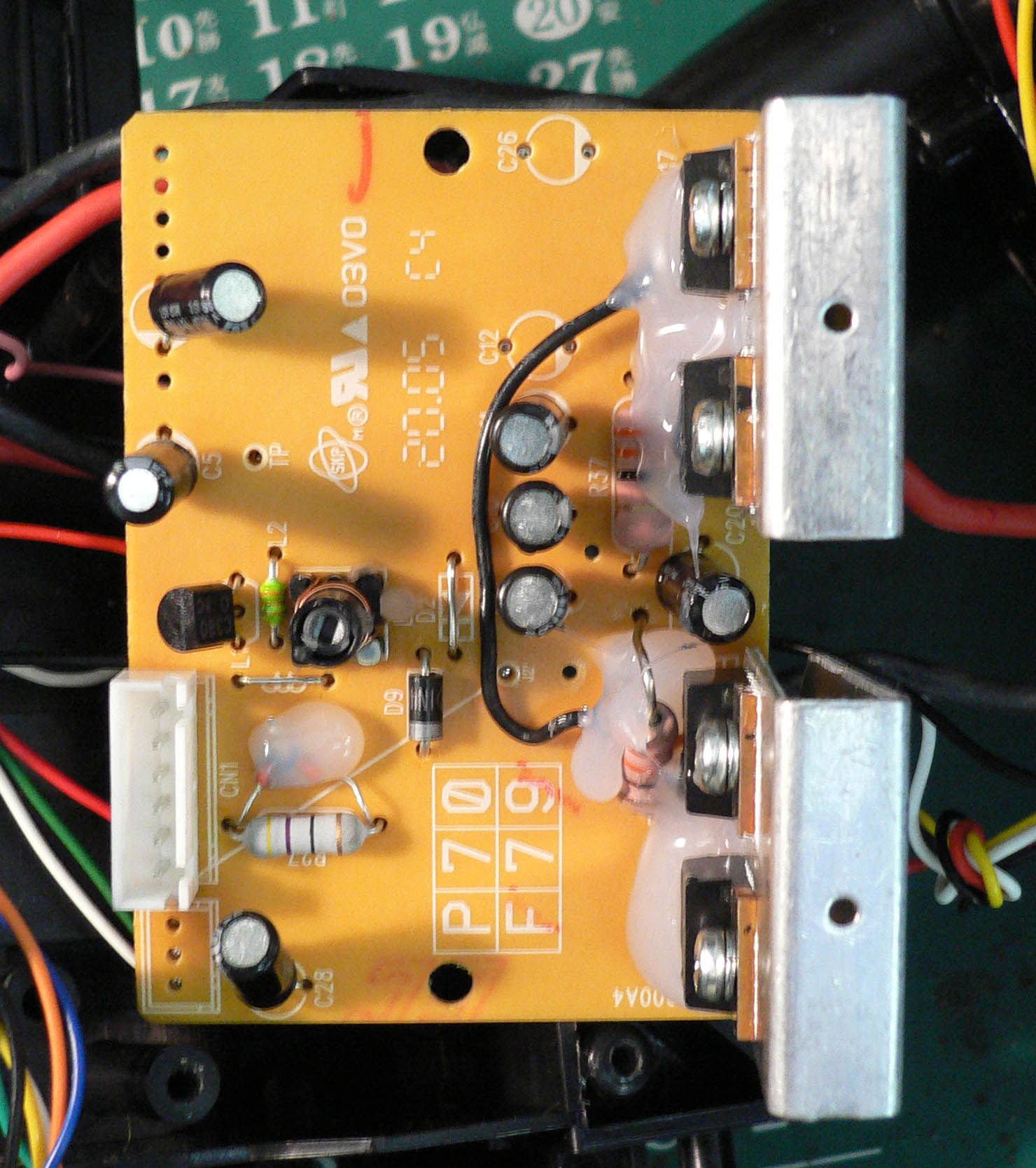
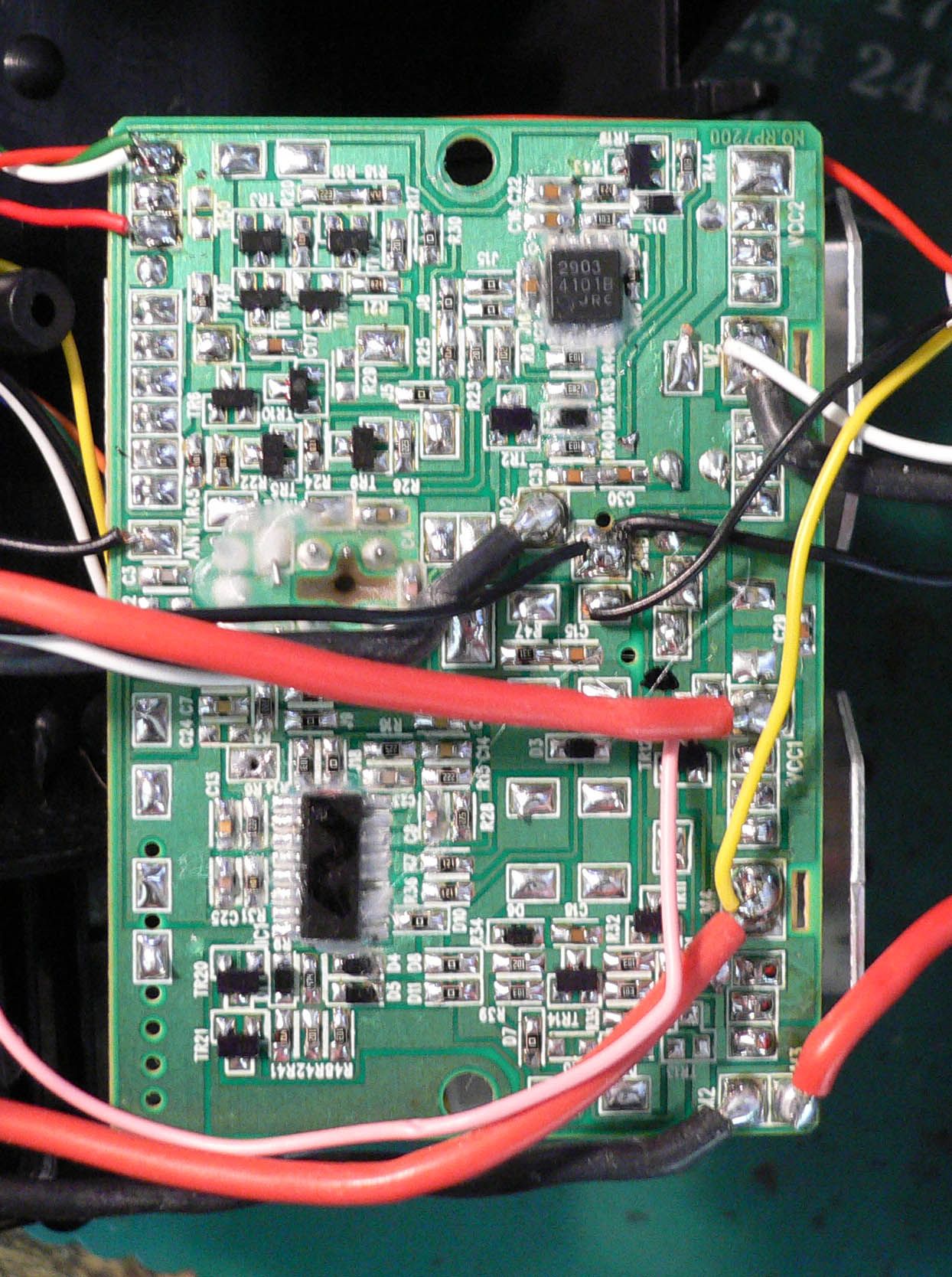
RP7200 CIRCUIT EXPLANATION FCC ID:CVTRP7200H 1) The Radio Frequency inputted through The ANT.,is passed to the Super regenerative receiver,formed by TR1, where the Action Signal is detected. 2)The Action Signal is decode in the Ic.,and are send to each output terminal. 3)TR11,12,14,15,16,17 and 18 form the power motor drive control circuit. IC2,TR2,3,4,5,6,7,8,9,10 and 19 form the steering control circuit. 4)Forward motion IC1.11P(Pin) is turned Hi,and TR11,15 and 18 are turned on to make a Forward drive. 5)Backward motion IC1.10P is turned Hi,and TR12,16 and 17 are turned on to make a backward drive. 6)Right turns IC1.6P is turned Hi,and TR2 is turned on, and the voltage of IC2.5P fall down. Then the voltage of IC2.5P fall down from the voltage of 6P, and IC2.7P is turned Low. When IC2.7P is turned Low,and TR4,5,10 and 22 are turned on to make a Right turn. 7)Left turns IC1.7P is turned Hi,and TR19 is turned on, and the voltage of IC2.3P fall down. Then the voltage of IC2.3P fall down from the voltage of 2P, and IC2.1P is turned Low. When IC2.1P is turned Low,and TR3,6,7 and 8 are turned on to make a Left turn. NIKKO CO.,LTD. R&D Dept. Manager Y.MAEDA
Parts List/Tune Up Info
NO.RP7200 PCB.PARTS LIST FCC ID:CVTRP7200H49.860MHz RX PCB NO.DESCRIPTIONCODEPARTS NAMENOTENO.DESCRIPTIONCODEPARTS NAMENOTE 1I.C.IC1RX2 73R341k 2IC2BA10339/F 74R351k 3TRANSISTORTR12SC380-O75R36120(1/10W) 4TR22SC1623L6 or equivalent76R3733(2W) 5TR32SA812 or equivalent77R3833(2W) 6TR4KTC8550 or equivalent78R3910k 7TR52SA812 or equivalent79R4010k 8TR6KTC8550 or equivalent80R414.7k 9TR72SA812 or equivalent81R421k 10TR8KTC8050 or equivalent82R4312K 11TR92SA812 or equivalent83R4410k 12TR10KTC8050 or equivalent84R45100k 13TR112SC1623L6 or equivalent85R4610k 14TR122SC1623L6 or equivalent86R47330 15TR13-87VR25kOUT OF PCB 16TR142SC1623L6 or equivalent88R4810k 17TR152SA1129K or equivalent89R49100k 18TR162SA1129K or equivalent90R50- 19TR172SC2654K or equivalent91CAPACITORC 1105(C) 20TR182SC2654K or equivalent92C 25p( C) 21TR192SC1623L6 or equivalent93C 333p(C) 22TR202SC1623L6 or equivalent94C 41p(C) 23TR212SC1623L6 or equivalent95C 54.7(E) 24DIODED 11N4148WS or equivalent96C 6222(B,X7R) 25D 20 Ohm wire97C 7103(B.X7R) 26D 3VZ3.3V98C 8471(B.X7R) 27D 41N4148WS or equivalent99C 9103(B.X7R) 28D 51N4148WS or equivalent100C10100(E) 29D 61N4148WS or equivalent101C11100(E) 30D 70 ohm102C12- 31D 80 ohm103C13222(C.X7R) 32D 91N4002 or equivalent104C14103(C.X7R) 33D100 ohm105C15104(C) 34D110 ohm106C16105(C) 35D121N4148WS or equivalent107C17104(C) 36D131N4148WS or equivalent108C18105(C) 37D141N4148WS or equivalent109C19100(E) 38D15VZ6.8V110C2010(NP) 39D16VZ6.8V111C21105(C) 40RESISTORR1150k112C22104(C) 41R2-113C2333(C) 42R3820114C24- 43R42.2K115C25471(B.X7R) 44R5-116C26- 45R62.2K117C27100(E) 46R7120(1/10W)118C28100(E) 47R81k119C29104(C) 48R9470k120C30104(C) 49R10680 121C31104(C) 50R1110k122INDUCTORL 1- 51R123.3K123L 2SP 3.3uH 52R136.8K 124L 3S6.5T 53R1410k125JUNPERJ10 ohm 5mm 54R152.2K126J30 ohm 60mm 55R162.2M127J50 ohm 56R171k128J80 ohm 57R184.7k129J90 ohm 58R1922k130J11- 59R20820(1/10W)131J120 ohm 60R21820(1/10W)132J150 ohm 61R22820(1/10W)133J160 ohm 62R231k134J180 ohm 63R24820(1/10W)135EXTRA PARTSEP 1Heat sink H-23 x2 64R254.7k136EP 2TP:3*8B(W/spring washer)x4 65R2622k137EP 2PCB No.RP7200 66R2747(1W)RESISTOR:No mark=(Discrete:1/6W,±5%, Chip:1/16W±5%) INDUCTOR:100mA,±10% 67R282.2MCAPACITOR (C):Ceramic,50WV,+80-20% (T):Tantalum,35WV,±10% 68R29- (M):Mylar,50WV[No mark=K.rank(±10%),J.rank(±5%)] 69R300 (E):Electrolytic,16WV,±20% (N):Non pole Electrolytic,16WV,±20% 70R31100k 71R3210k 72R3310k
Parts List/Tune Up Info
Sheet2 SPEED MASTER X21 MAIN PCB 2003.11.20 tk. NO.DESCRIPTIONCODENormal versionTimer cut off version 1IC.IC124LC64T-I/ST(TSSOP)SII 2IC2NJM2903V(SSOP)JRC 3IC3HT48R70AHOLTEC 4IC4NJU26150FR1JRC 5IC5NJUMU7223DL1-50-TE1JRC 6IC6NJM2871AF25-TE1JRC 7IC7SN74LX125ATI 8IC9AK5355VTAKM 9TRANSISTORTR12SC1623L6 or equivalent 10TR2KTC8550 or equivalent 11TR3KTC8050 or equivalent 12TR4KTC8550 or equivalent 13TR52SC1623L6 or equivalent 14TR92SC1623L6 or equivalent 15TR102SC1623L6 or equivalent 16TR152SC1623L6 or equivalent 17TR162SC1623L6 or equivalent 18 DIODE D61N4148WS or equivalent 19D71N4148WS or equivalent 20D92FW-J42 or equivalentSCHOTTKY 21D141N4148WS or equivalent 22RESISTORR1100k 1608 type 23R2100k 1608 type 24R3100k 1608 type 25R4100k 1608 type 26R5100k 1608 type 27R6100k 1608 type 28R7100k 1608 type 29R8100k 1608 type 30R91k 1608 type 31R101k 1608 type 32R1110k 1608 type 33R12330 1608 type 34R13330 1608 type 35R141.8k 1608 type 36R153.3k 1608 type 37R161.8k 1608 type 38R1710 1608 type - 1 - Sheet2 39R1810k 1608 type 40R19100k 1608 type 41R204.7k 1608 type 42R211M 1608 type 43R22100 1608 type 44R2310k 1608 type 45R248.2k 1608 type - 2 - Sheet2 NO.DESCRIPTIONCODENormal versionTimer cut off version 46R2510k 1608 type 47R268.2k 1608 type 48R271k 1608 type 49R314.7k 1608 type 50R3547 1608 type 51R3647 1608 type 52R3747 1608 type 53R3847 1608 type 54R391k 1608 type 55R4027k 1608 type 56R4110k 1608 type 57R4227k 1608 type 58R4310k 1608 type 59R441k 1608 type 60R4510k 1608 type 61R4647 1608 type 62R4710k 1608 type 63R4810k 1608 type 64R4910k 1608 type 65R5010k 1608 type 66R53330k 1608 type 67R5810k 1608 type 68R5910k 1608 type 69CAPACITORC1105(C) 1608 type 70C2105(C) 1608 type 71C3105(C) 1608 type 72C4105(C) 1608 type 73C5100(E) small 74C6104(C) 1608 type 75C7100(E) small 76C8103(C) 1608 type 77C9104(C) 1608 type 78C1010(E) small 79C1110(E) small 80C1210p(C) 1608 type 81C1310p(C) 1608 type 82C14105(C) 1608 type 83C15104(C) 1608 type - 3 - Sheet2 84C1610(E) small 85C17104(C) 1608 type 86C18104(C) 1608 type 87C19104(C) 1608 type 88C20104(C) 1608 type 89C21104(C) 1608 type 90C2210p(C) 1608 type - 4 - Sheet2 NO.DESCRIPTIONCODENormal versionTimer cut off version 91C23102(C) 1608 type 92C2412p(C) 1608 type 93C25103(C) 1608 type 94C26103(C) 1608 type 95C2710(E) small 96C2810(E) small 97C29103(C) 1608 type 98C30103(C) 1608 type 99C32104(C) 1608 type 100C3310p(C) 1608 type 101C3410(E) small 102C3510(E) small 103C36104(C) 1608 type 104C37104(C) 1608 type 105C382.2(E) small 106C39104(C) 1608 type 107C4010(E) TANTAL 108C4210p(C) 1608 type 109C43150p(C) 1608 type 110C4410p(E) small 111INDUCTORL12.2uH 112JAMPER *AJ10O 113*AJ20O 114*AJ30O 115*AJ50O 116*AJ60O 117EXTRA PARTSEP1X1:X'TAL 8MHzAT-38 118EP2X2:X'TAL 33.6888MHzAT-49 119EP3BUZZER JV-27T4EJOINT VICTORY 120EP5TACT SW : IT-1102SW1,2,3,4,5 LUCKY FIRST KNOB=4.3 121EP6CONNECTER : A1501WR0-8PCON1 JWT 122EP7CONNECTER : A1501WR0-9PCON2 JWT 123EP8CONNECTER : A1501WR0-3PCON3 JWT 124EP9LCD:OPTO0164CTCASIL 125EP9PCB:No.SG-0015 both surface PCB(glass) RESISTOR:1608 type chip,1/16W,±5% INDUCTOR:100mA,±10% CAPACITOR(C):Ceramic,1608 type chip,50WV,+-10% (T):Tantalum,35WV,±10% (M):Mylar,50WV[No mark=K.rank(±10%),J.rank(±5%)] - 5 - Sheet2 (E):Electrolytic,16WV,±20% (N):Non pole Electrolytic,16WV,±20% - 6 -
Test Report
JAPAN QUALITY ASSURANCE ORGANIZATION 21-25, KINUTA 1-CHOME, SETAGAYA-KU, TOKYO 157-8573 JAPAN PHONE (03) 3416-0111, FAX (03) 3416-9691 JQA File No. : 400-50236 Issue Date : June 30, 2005 Page 1 of 25 EMI TEST REPORT JQA File No. : 400-50236 Model No. : RP7200H Type of Equipment : Radio Controlled Toy (Superregenerative Type) Regulations Applied : CFR 47 FCC Rules and Regulations Part 15 FCC ID : CVTRP7200H Applicant : NIKKO CO., LTD. Address : 1-7-14, Mizumoto, Katsushika-ku, Tokyo 125-0032, Japan Manufacturer : NIKKO ELECTRONICS BHD. Address : Plot 497, Prai Free Trade Zone, Prai Industrial Estate, Prai, Penang, Malaysia. 13600 Received date of EUT : June 20, 2005 Final Judgment : Passed Test results in this report are obtained in use of equipment that is traceable to National Institute of Advanced Industrial Science and Technology (AIST) of Japan and National Institute of Information and Communications Technology (NICT) of Japan. The test results only respond to the tested sample. This report should not be reproduced except in full, without the written approval of JQA EMC Engineering Dept. Testing Div. JQA File No. :400-50236 FCC ID :CVTRP7200H Model No. :RP7200H Issue Date :June 30, 2005 Standard :CFR 47 FCC Rules Part 15 Page 2 of 25 JAPAN QUALITY ASSURANCE ORGANIZATION TABLE OF CONTENTS Page 1 Documentation 1.1 Test Regulation 3 1.2 General Information 3 1.3 Test Condition 4 – 7 1.4 EUT Modifications / Deviation from Standard 8 1.5 Test results / Uncertainty 9 1.6 Summary 10 1.7 Test Configuration / Operation of EUT 11 1.8 EUT Arrangement (Drawings) 12 1.9 Preliminary Test and Test-setup (Drawings) 13 – 16 1.10 EUT Arrangement (Photographs) 17 2 Test Data 2.1 AC Power Line Conducted Emission N/A 2.2 Radiated Emission (Electric Field) 18 – 20 2.3 Antenna Conducted Power N/A 3 Appendix Test instruments List 21 – 25 JQA File No. :400-50236 FCC ID :CVTRP7200H Model No. :RP7200H Issue Date :June 30, 2005 Standard :CFR 47 FCC Rules Part 15 Page 3 of 25 JAPAN QUALITY ASSURANCE ORGANIZATION 1 DOCUMENTATION 1.1 TEST REGULATION FCC Rules and Regulations Part 15 Subpart A and B Superregenerative Receiver Test procedure : AC power line conducted emission, radiated emission and antenna conducted power tests were performed according to the procedures in ANSI C63.4-2003. 1.2 GENERAL INFORMATION 1.2.1 Test facility : 1) Test Facility located at EMC Engineering Dept. Testing Div. : - No.2 and 3 Anechoic Chambers( 3 meters Site ). - Shielded Enclosure. 2) EMC Engineering Dept. Testing Div. is recognized under the National Voluntary Laboratory accreditation Program for satisfactory compliance established in title 15, Part 285 Code of Federal Regulations. NVLAP Lab Code : 200189-0 1.2.2 Description of the Equipment Under Test (EUT) : 1) Type of Equipment : Radio Controlled Toy 2) Product Type : Production 3) Category : Superregenerative Receiver 4) EUT Authorization : Certification 5) FCC ID : CVTRP7200H 6) Trade Name : NIKKO 7) Model No. : RP7200H 8) Tuning Frequency Range : 49.830 MHz – 49.890 MHz 9) Highest Frequency Used in the EUT : - 10) Serial No. : None 11) Date of Manufacture : None 12) Power Rating : 7.2VDC (Battery pack) 13) EUT Grounding : None 1.2.3 Definitions for symbols used in this test report : x - indicates that the listed condition, standard or equipment is applicable for this report. - indicates that the listed condition, standard or equipment is not applicable for this report. JQA File No. :400-50236 FCC ID :CVTRP7200H Model No. :RP7200H Issue Date :June 30, 2005 Standard :CFR 47 FCC Rules Part 15 Page 4 of 25 JAPAN QUALITY ASSURANCE ORGANIZATION 1.3 TEST CONDITION 1.3.1 The measurement of the AC Power Line Conducted Emission - was performed in the following test site. x - was not applicable. Test location : Safety & EMC Center EMC Engineering Dept. Testing Div. 21-25, Kinuta 1-chome, Setagaya-ku, Tokyo 157-8573, Japan - Shielded Enclosure - Anechoic Chamber No. 2 (portable Type) Used test instruments : Type Number of test instruments (Refer to Appendix) Test Receiver N/A Spectrum Analyzer N/A Cable N/A AMN(for EUT) N/A AMN(for Peripheral) N/A Termination N/A JQA File No. :400-50236 FCC ID :CVTRP7200H Model No. :RP7200H Issue Date :June 30, 2005 Standard :CFR 47 FCC Rules Part 15 Page 5 of 25 JAPAN QUALITY ASSURANCE ORGANIZATION 1.3.2 The measurement of the Radiated Emission(30 MHz – 1000 MHz) x - was performed in the following test site. - was not applicable. Test location : Safety & EMC Center EMC Engineering Dept. Testing Div. 21-25, Kinuta 1-chome, Setagaya-ku, Tokyo 157-8573, Japan - Anechoic Chamber No. 2 (3 meters) x - Anechoic Chamber No. 3 (3 meters) Validation of Site Attenuation : 1) Last Confirmed Date :March, 2005 2) Interval :1 year Used test instruments : Type Number of test instruments (Refer to Appendix) Test Receiver TR06 Antenna AN03, AN07, AN09 Cable CA02 RF Amplifier N/A Signal Generator SG05 JQA File No. :400-50236 FCC ID :CVTRP7200H Model No. :RP7200H Issue Date :June 30, 2005 Standard :CFR 47 FCC Rules Part 15 Page 6 of 25 JAPAN QUALITY ASSURANCE ORGANIZATION 1.3.3 The measurement of the Radiated Emission(Above 1000 MHz) - was performed in the following test site. x - was not applicable. Test location : Safety & EMC Center EMC Engineering Dept. Testing Div. 21-25, Kinuta 1-chome, Setagaya-ku, Tokyo 157-8573, Japan - No. 2 site (3 meters) - No. 3 site (3 meters) Validation of Site Attenuation : 1) Last Confirmed Date :March, 2005 2) Interval :1 year Used test instruments : Type Number of test instruments (Refer to Appendix) Test Receiver N/A Spectrum Analyzer N/A Cable N/A Antenna N/A RF Amplifier N/A JQA File No. :400-50236 FCC ID :CVTRP7200H Model No. :RP7200H Issue Date :June 30, 2005 Standard :CFR 47 FCC Rules Part 15 Page 7 of 25 JAPAN QUALITY ASSURANCE ORGANIZATION 1.3.4 The measurement of the Antenna Conducted Power - was performed in the following test site. x - was not applicable. Test location : Safety & EMC Center EMC Engineering Dept. Testing Div…
Text truncated - open the document above for the full version.
Test Setup Photos
JQA File No. :400-50236 FCC ID :CVTRP7200H Model No. :RP7200H Issue Date :June 30, 2005 Standard :CFR 47 FCC Rules Part 15 Page 17 of 25 JAPAN QUALITY ASSURANCE ORGANIZATION 1.10 TEST ARRANGEMENT (PHOTOGRAPHS) PHOTOGRAPHS OF EUT CONFIGURATION FOR RADIATED EMISSIONS MEASUREMENT Photograph present configuration with maximum emission
Contact Information
Applicant
Minori Oohira
81-3 3609-0900Fax: 81 3-3609-1033
Test Firm
Japan Qlty. Assur. Org. Kitakansai Testing CenterHiroyuki Nakamura
Technical Specifications
| # | Rule Parts | Frequency Range | Power Output |
|---|---|---|---|
| 1 | 15B | 49.83 MHz - 49.89 MHz | - |
Other Applications from Nikko Co Ltd
CVTTA7752
Mar 12, 2008Radio Controlled Toy
Equipment Class
DXX - Part 15 Low Power Communication Device Transmitter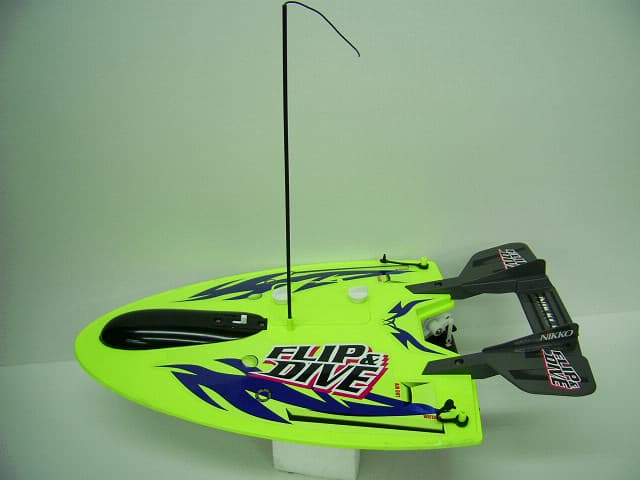
CVTRA4040H
Mar 12, 2008Radio Controlled Toy
Equipment Class
CYY - Communications Receiver used w/Pt 15 Transmitter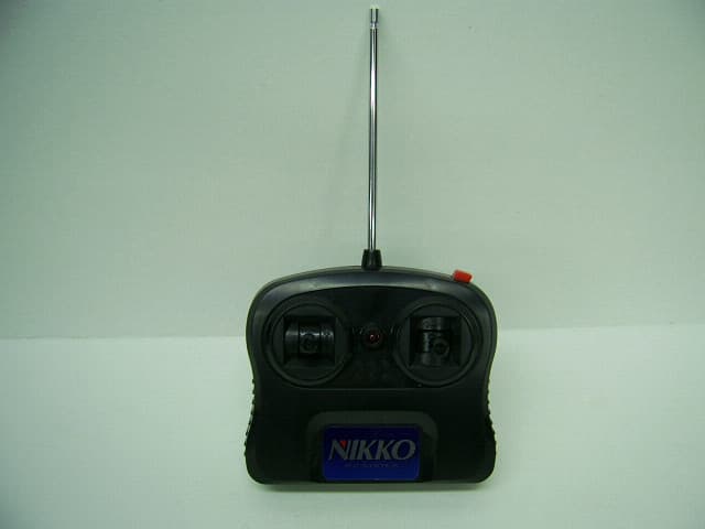
CVTTP7752H
Mar 12, 2008Radio Controlled Toy
Equipment Class
DXX - Part 15 Low Power Communication Device Transmitter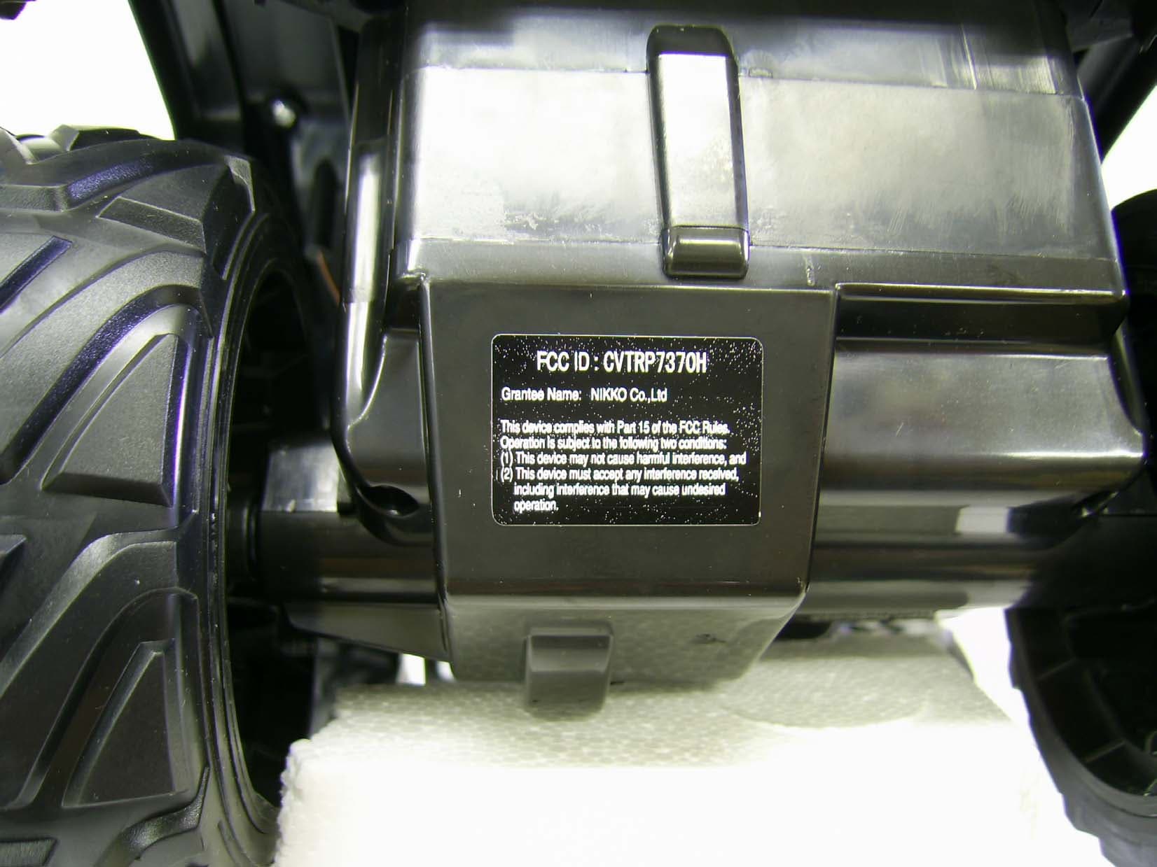
CVTRP7370H
Jul 24, 2007Radio Controlled Toy Receiver
Equipment Class
CYY - Communications Receiver used w/Pt 15 Transmitter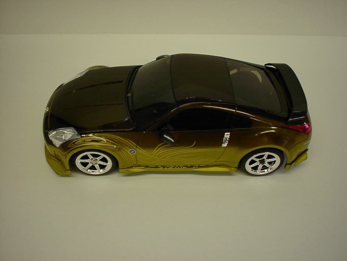
CVTRP7340H
Jan 28, 2007Radio Controlled Toy
Equipment Class
CRR - Superregenerative Receiver