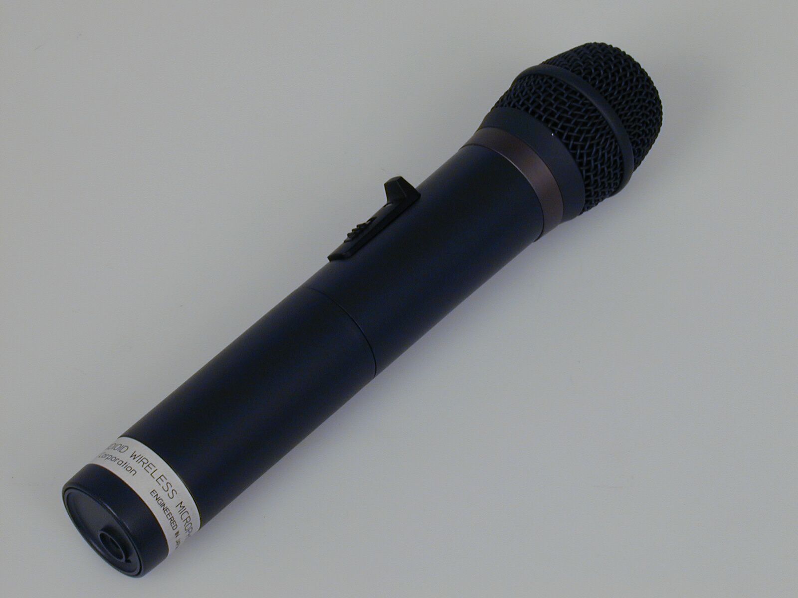
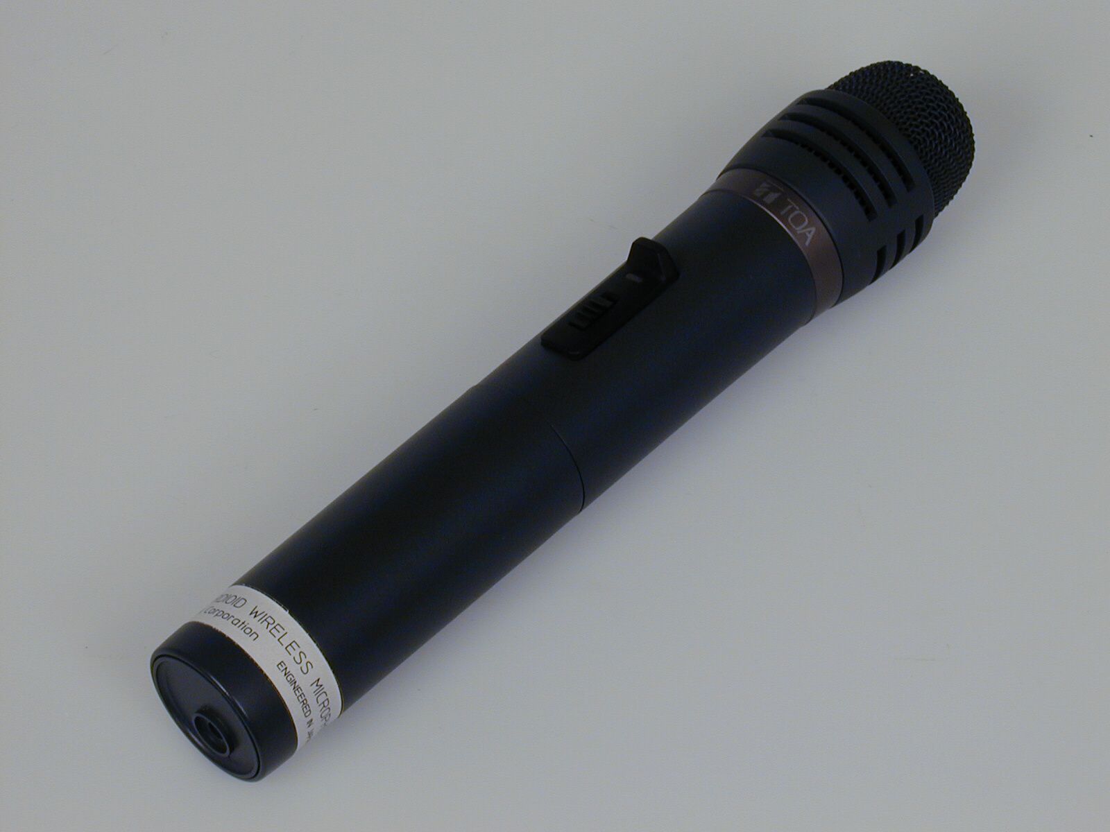
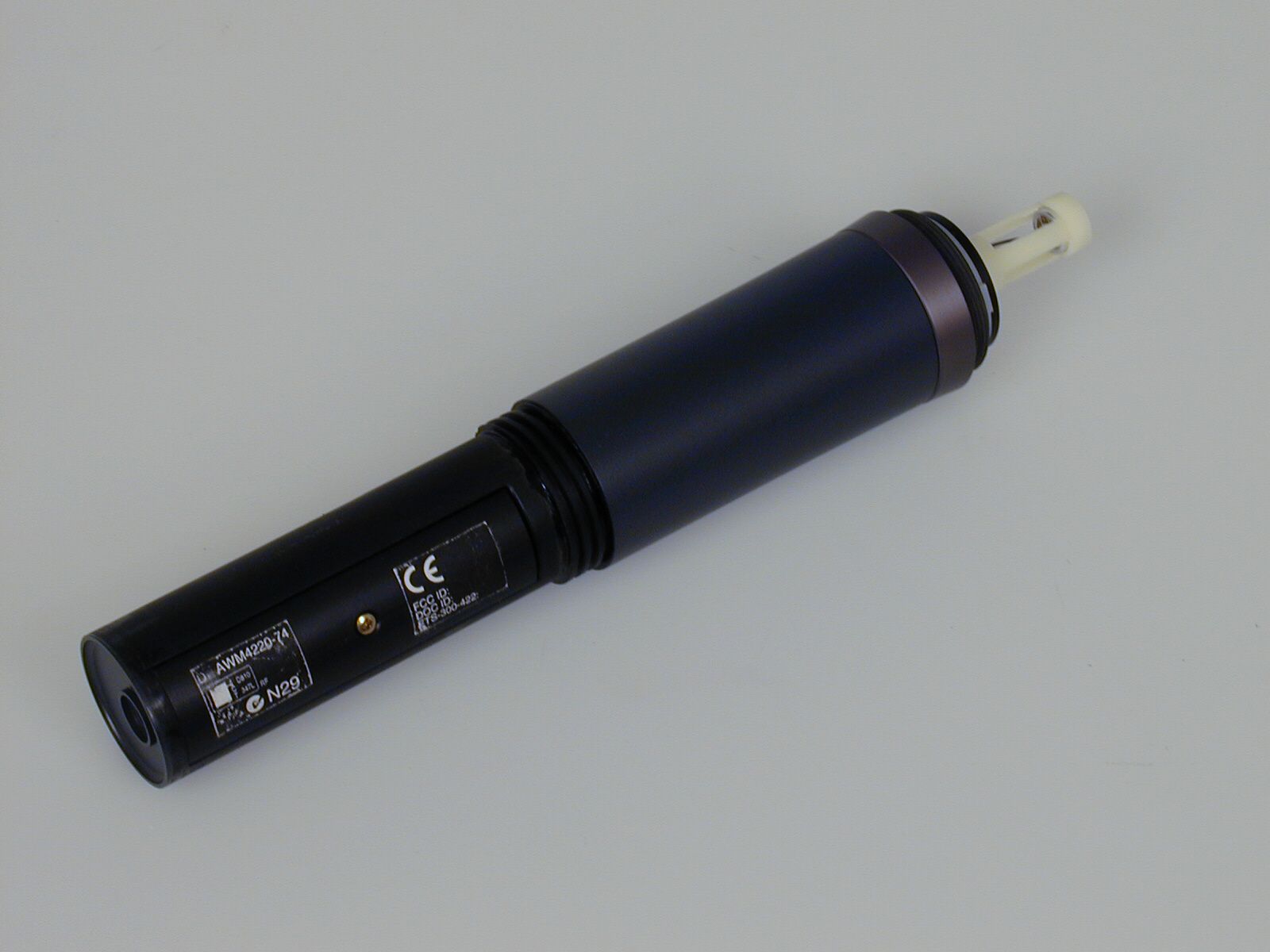
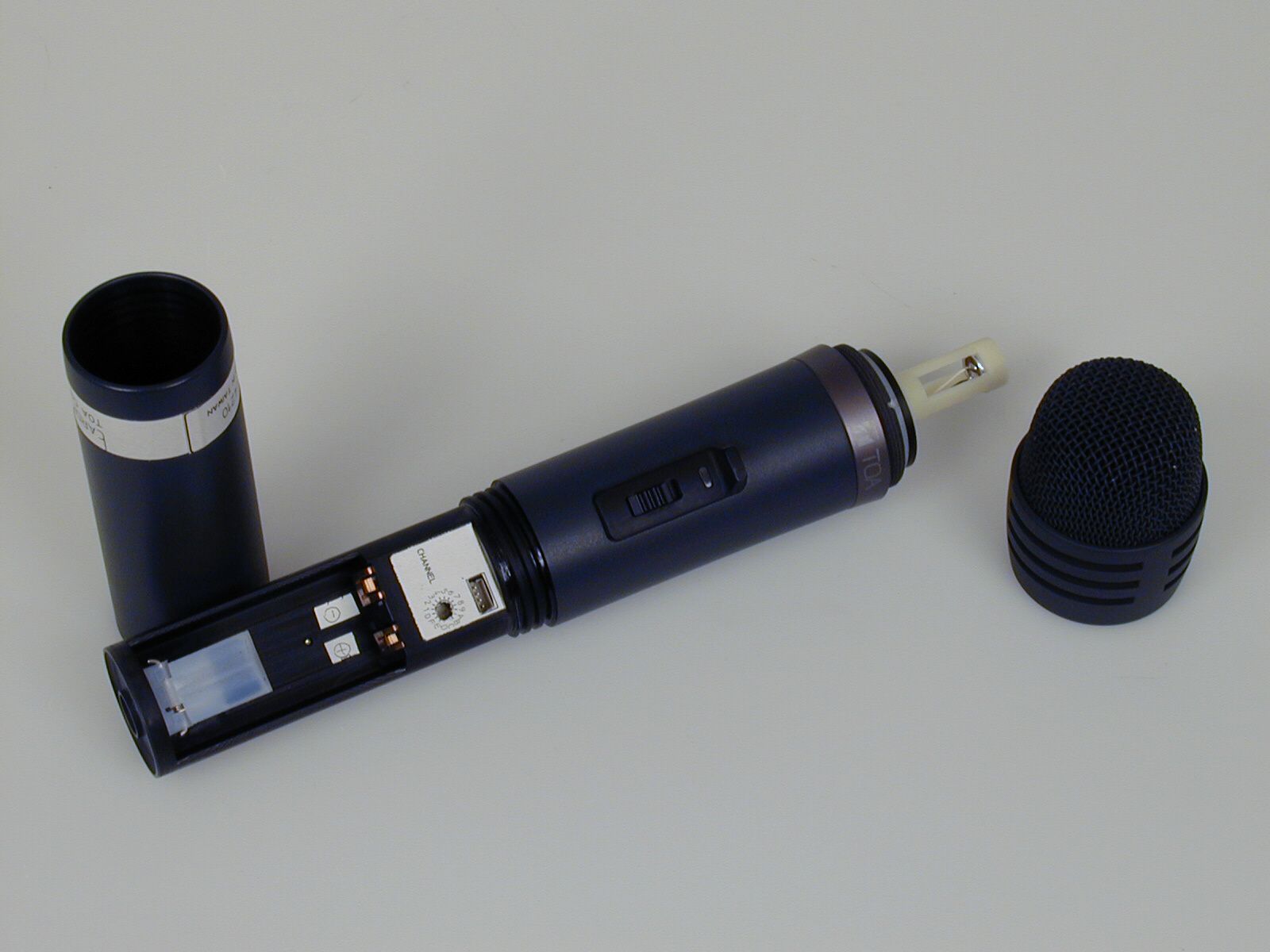
DLAWM-4210-4220Wireless Microphone
TOA Corporation
Click to zoom
Application Details
- Equipment Class
- TBF - Licensed Broadcast Transmitter Held to Face
- Date of Grant
- Aug 24, 2000
- Application Purpose
- Original Equipment
- Date of Application
- May 18, 2000
- Equipment Note
- Wireless Microphone
- Frequency Range
- 614.00000000 - 806.00000000
- Company
- TOA Corporation
- Country
- Japan
Documents & Files
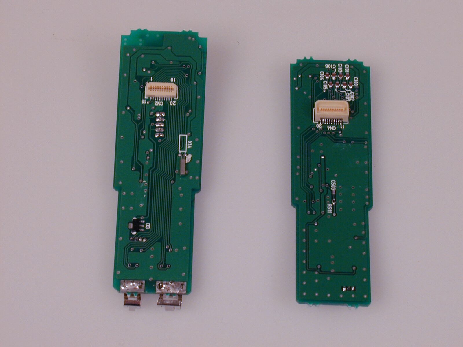
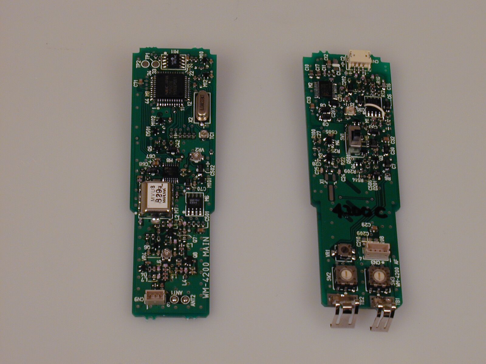
Document Text
Text extracted from the exhibit documents filed with the FCC. Open a document above to read the original.
Users Manual
11 9. OPERATING INSTRUCTIONS TOA WIRELESS MICROPHONE model WM-4210 General description The WM-4210 hand held wireless microphone has been manufactured for use with a UHF system. It incorporates a cardioid pick-up pattern and has been designed for use in vocal and speech reinforcement applications. The built-in compressor -expander circuit minimizes the influence from ambient noise. Battery insertion 1)Hold the microphone body and rotate the microphone grip counterclockwise. The microphone grip is designed to be completely removed from the body. 2)The battery compartment accepts one 6LR61 battery. Please insert the battery according to the instructions attached to the inside of the battery compartment. Please observe correct polarity when inserting the battery. 3)Replace the microphone grip by sliding and relightening it clockwise . Operating the microphone 1)Make sure that the receiver and the wireless microphone are of the same channel(frequency). 2)If they are not identical in channel(frequency),you have to adjust the bank and channel switches. 3)Place the microphone ON/OFF switch in the ON position. The orange LED indicates the circuit is active. 4)Make sure to shift the ON/OFF switch back to the off position after using the WM-4210 wireless microphone. Battery replacement 1)A brand-new battery will provide the power for enough to operate the unite continuously for 10 hours . 2)As long as the battery has sufficient power for the microphone to function properly, the orange LED will light. When the orange LED starts to fade and then flashing, replace it with a new one. Operational Hints (1) The microphone's service distance is 3-150 m. When the microphone user moves in a facility, signal dropouts (momentary losses of signal reception) may be encountered. These dropouts are caused by the building's architectural designs or materials which block the travel of or reflect the radio signal. If this occurs, the user needs to change locations for better signal reception. (2) The proper operation of your wireless system may be interfered with by other system operating on the same frequency. In such cases, change the operating frequency of your system. It is recommended that the Scan function (of the WT-4800) be used to avoid the frequency interference, which always searches and shows idle frequencies. (3) Should you have any questions regarding the use or availability of TOA wireless products, please contact your local TOA dealer. Audio level This wireless microphone is designed to satisfy the most of the popular vocalists. The audio level is set at 130dBspl . 12 ModelWM-4210 Carrier Frequency 16 frequencies (Selectable from 690 MHz and 806 MHz) Frequency StabilityLess than 0.005% OscillatorCrystal-controlled PLL-synthesizer Modulation System Reactance modulation RF Carrier Power Less than 50mW Effective Radiated Power Less than 10mW Maximum Input Level130dBspl Maximum Deviation±40kHz Microphone ElementUnidirectional dynamic microphone Frequency Response50 to 15000Hz Pre-emphasis 50 μsec Antenna Whip antenna (Internal) Battery Type 6LR61(Alkaline 9V) Battery Life More than 10 hours Current Consumption 50mA TYP.(at 9.0V) Ambient Temperature14°F to 122°F (–10°C to 50°C) Tone Frequency 32.768 kHz Controls Power ON/OFF, Bank and Channel select, BatteryChecker, illegal Channel ColorBlack Dimensionsø1.5" X 8.76"(ø38 X 222.5mm) Weight 0.594 lbs.(270g) with battery Specifications FCC license requirement FCC This system requires a FCC license for legal operation. Obtain the application form FCC at the address listed on the form and mail it to the FCC after completing it, following the instructions below. When the application is approved, the FCC will mail the license to you.
Users Manual
11 9. OPERATING INSTRUCTIONS TOA WIRELESS MICROPHONE model WM-4220 General description The WM-4220 hand held wireless microphone has been manufactured for use with a UHF system. It incorporates a cardioid pick-up pattern and has been designed for use in speech reinforcement applications. The built-in compressor -expander circuit minimizes the influence from ambient noise. Battery insertion 1)Hold the microphone body and rotate the microphone grip counterclockwise. The microphone grip is designed to be completely removed from the body. 2)The battery compartment accepts one 6LR61 battery. Please insert the battery according to the instructions attached to the inside of the battery compartment. Please observe correct polarity when inserting the battery. 3)Replace the microphone grip by sliding and relightening it clockwise . Operating the microphone 1)Make sure that the receiver and the wireless microphone are of the same channel(frequency). 2)If they are not identical in channel(frequency),you have to adjust the bank and channel switches. 3)Place the microphone ON/OFF switch in the ON position. The orange LED indicates the circuit is active. 4)Make sure to shift the ON/OFF switch back to the off position after using the WM-4220 wireless microphone. Battery replacement 1)A brand-new battery will provide the power for enough to operate the unite continuously for 10 hours . 2)As long as the battery has sufficient power for the microphone to function properly, the orange LED will light. When the orange LED starts to fade and then flashing, replace it with a new one. Operational Hints (1) The microphone's service distance is 3-150 m. When the microphone user moves in a facility, signal dropouts (momentary losses of signal reception) may be encountered. These dropouts are caused by the building's architectural designs or materials which block the travel of or reflect the radio signal. If this occurs, the user needs to change locations for better signal reception. (2) The proper operation of your wireless system may be interfered with by other system operating on the same frequency. In such cases, change the operating frequency of your system. It is recommended that the Scan function (of the WT-4800) be used to avoid the frequency interference, which always searches and shows idle frequencies. (3) |Should you have any questions regarding the use or availability of TOA wireless products, please contact your local TOA dealer. Audio level This wireless microphone is designed to satisfy the most of the popular presenters. The audio level is set at 125dBspl . 12 ModelWM-4220 Carrier Frequency 16 frequencies (Selectable from 690 MHz and 806 MHz) Frequency StabilityLess than 0.005% OscillatorCrystal-controlled PLL-synthesizer Modulation System Reactance modulation RF Carrier Power Less than 50mW Effective Radiated Power Less than 10mW Maximum Input Level125dBspl Maximum Deviation±40 kHz Microphone ElementUnidirectional erectlet condenser microphone Frequency Response100 to 15000 Hz Pre-emphasis 50 μsec Antenna Whip antenna (Internal) Battery Type 6LR61(Alkaline 9V) Battery Life More than 10 hours Current Consumption 50mA TYP.(at 9.0V) Ambient Temperature14°F to 122°F (–10°C to 50°C) Tone Frequency 32.768 kHz Controls Power ON/OFF, Bank and Channel select, BatteryChecker, illegal Channel ColorBlack Dimensionsø”1.5" X 8.76"(ø38 X 222.5mm) Weight 0.594 lbs.(250 g) with battery Specifications FCC license requirement FCC This system requires a FCC license for legal operation. Obtain the application form FCC at the address listed on the form and mail it to the FCC after completing it, following the instructions below. When the application is approved, the FCC will mail the license to you.
Block Diagram
6 6. BLOCK DIAGRAM +B: DC 5V LOOPFIL. CHANNELSET VOLTAGEDETECTORM10: S-80842ANNP SW OFF DETECT MUTE SW. BIAS SW. BAT CHECKER X1:32.768KHz X2: 6.000MHz RESET FREQ. SET DATA POWER ON / OFF SW BATT.6LR61DC9V RFLPF RF AMP.Q7:2SC3356 D1: DA204U BIASREGULATOR VCOM7:MVUS MIC AMP.M1,: NJM2115M TONE OSC.M3: TC4SU69F FREQUENCYSYNTHESIZERM8: LMX2316 BIAS SW.Q6:2SA1622 PAD CPUM9: PD750004GB BAT. CHECKERQ2: 2SC4211D2: LED MIC CPU CPU REG. CONT./SW OFF DETECTQ1,3,4: 2SC4211 RF P.A.Q8:2SC3356 VOLTAGE DETECTM102: S-80855ANNP CLOCK BUFFERM12: TC7S04FU VR4RF POWER ADJ. D4 VR2DEV. ADJ. PRE EMPHASISM1: NJM2115M COMPRESSERM2:SA575DK L.P.F.M2:SA575DK TONE BUFFERM4: TC4SU69F MUTE SW.M101:TC7S66FU PLL LOOP VCO SW.Q5:2SA1622 CPU REGULATORM5: TK11250MTL CPU LOW VOLTAGE DETECT REFERENCECLOCK OSC FREQ.ADJ. EEPROMM11: 24C16 FREQ. DATAWRITE VCO. SW. 2 3 1 45 6 9 12 13 14 15 16 17 11 10 29 19 27 23 24 25 26 20 22 28 18
Block Diagram
6 6. BLOCK DIAGRAM +B: DC 5V LOOPFIL. CHANNELSET VOLTAGEDETECTORM10: S-80842ANNP SW OFF DETECT MUTE SW. BIAS SW. BAT CHECKER X1:32.768KHz X2: 6.000MHz RESET FREQ. SET DATA POWER ON / OFF SW BATT.6LR61DC9V RFLPF RF AMP.Q7:2SC3356 D1: DA204U BIASREGULATOR VCOM7:MVUS MIC AMP.M1,: NJM2115M TONE OSC.M3: TC4SU69F FREQUENCYSYNTHESIZERM8: LMX2316 BIAS SW.Q6:2SA1622 PAD CPUM9: PD750004GB BAT. CHECKERQ2: 2SC4211D2: LED MIC CPU CPU REG. CONT./SW OFF DETECTQ1,3,4: 2SC4211 RF P.A.Q8:2SC3356 VOLTAGE DETECTM102: S-80855ANNP CLOCK BUFFERM12: TC7S04FU VR4RF POWER ADJ. D4 VR2DEV. ADJ. PRE EMPHASISM1: NJM2115M COMPRESSERM2:SA575DK L.P.F.M2:SA575DK TONE BUFFERM4: TC4SU69F MUTE SW.M101:TC7S66FU PLL LOOP VCO SW.Q5:2SA1622 CPU REGULATORM5: TK11250MTL CPU LOW VOLTAGE DETECT REFERENCECLOCK OSC FREQ.ADJ. EEPROMM11: 24C16 FREQ. DATAWRITE VCO. SW. 2 3 1 45 6 9 12 13 14 15 16 17 11 10 29 19 27 23 24 25 26 20 22 28 18
Operational Description
7 7. CIRCUIT EXPLANATION HOW EACH SECTION WORKS We will explain operations of each section based on block diagrams. (1) MICROPHONE (Block diagram No. 1) An internal microphone is of unidirectional dynamic type. Impedance: 600 Ω Sensitivity: -52 dB (1kHz, 0 dB = 1 V/1 pa) (2) MICROPHONE AMPLIFIER (2) The microphone amplifier uses an OP amp (M1) and amplifies the signal from the microphone capsule to the level necessary for the compressor circuit. (3) COMPRESSOR (3) The compander IC is SA575DK (M2), and has a compressor circuitry and 2 OP amps. The compression ratio is 1/2 (logarithmic compression). (4) PRE-EMPHASIS (4) Pre-emphasis is carried out to improve the system's S/N ratio. Amplifier (M1) is used as an OP amp. A time constant if 50 μsec. (5) LPF (5) The third Butterworth type low-pass filter is constructed using the OP amp built in M2 to attenuate the audio signal components of over 15 kHz. Also, the harmonic components of the tone signal to be superimposed in the LPF circuit are attenuated by the-pass filter.. (6) MUTE SW (6) Using the analog switch (M101), this circuit mutes both the audio and tone signals during the periods of from the power switch-on to the commencement of signal transmission and from power switch-off to transmission termination to operate the receiver tone squelch. (7) TONE OSC(7, 8) Consists of a quarts oscillator (X1) and an inverter (M3) and oscillates a signal for tone squelch (tone signal). The oscillation frequency is 32.768 kHz, and the output signal is taken out through a buffer (M4). (8) PLL FREQUENCY SYNTHESIZER (9, 10, 11) VCO (M7), PLL IC (M8) and LOOP FILTER make up a phase locked loop. The VCO oscillates the transmission frequency directly and divides the output. It then compares the frequency phase by means of the 25 kHz comparison frequency, and outputs a pulse corresponding to the phase difference. The pulse is applied to the VCO as a control voltage after integrated at a loop filter, and then is locked to the set transmission frequency. Both the audio and tone signals are input from the VCO's modulation terminal, and then are frequency-modulated. The modulation method is a reactance modulation system using a variable capacitance diode. (9) RF AMP, RF POWER AMP (12,13, 14) By amplifying the VCO's oscillation output with a transistor, these amplifiers not only make up for losses in a pad or RF LPF, but also gain the antenna power. The two-stage construction method is employed for the amplifiers to obtain sufficient buffer effects for the VCO, and a 6 dB pad is installed in the amplifier input. The output is less than 50 mW, and is adjusted by changing Q8's bias current using VR4 to change operation points. (10) BIAS REGULATOR, BIAS SWITCH (15, 16) By compensating for the temperature by means of a diode (D4), the bias circuit suppresses the changes of operation points due to temperature variations. When the VCO's transmission frequency becomes stable after PLL lockup completion, the switch (Q6) turns on and the bias is applied for radio signal transmission. (11) RF LPF (17) A 3-stage πtype low-pass filter is used for the RF section's band limiting filter to suppress the spurious- 8 radiated signals with frequencies much different from the transmission frequency. (12) CPU and its peripheral parts (18, 19, 20, 21, 22) This section is comprised of the CPU (M9), voltage detector (M10) and crystal-controlled reference oscillator (X2). The reference oscillator is 6.0 MHz in frequency, and is oscillated by the CPU's internal inverter to operate the CUP as a clock. At the same time, the 6 MHz signal is supplied to the PLL IC via the buffer (M12) as the PLL reference oscillation frequency. The oscillation frequency is adjusted by TCI so that its deviation stays within ±1 kHz. After its power switch is set to the ON position, the CPU controls the transmission frequency setting, the start of transmission, actions till voice transmission, and actions when the system is switched off. The operating procedures are stored in the CPU's mask ROM, and the control contents are as follows: (A) The CPU reads transmission frequency setting data from both the Bank and Channel setting switches, and transmits data to PLL IC for the division ratio setting. (B) The CPU controls the bias circuitry and Q6 so that the radio signal is not transmitted until the transmission frequency becomes stable. (C) The CPU controls MUTE SW, VCO SW, BIAS SW, and BATT.CHECKER. When the circuit voltage drops below 4.2 V, the voltage detector transmits a reset signal to the CPU to stop the CPU's operation so that no radio signal is transmitted. (13) REG.CONT/SW OFF DETECT (23, 24, 29) Setting the power switch to the ON position turns on Q3, and adds the control voltage to a regulator (M5) for its operation. As a result, the voltage of 5 VDC is supplied to each circuit all circuits begin to operate. If the power switch is set to the OFF position, both Q1 and Q4 transmit the SW OFF DETECT signal to the CPU and the tone signal is muted (M101) to enable the receiver's tone squelch. Both Q5 and Q6 then turn off, and the radio signal transmission stops. During this process, M5 continues to operate according to time constants of both C30 and R31. One second after the signal transmission stops, when R31's terminal voltage becomes lower than M5's operating voltage, M5 and all other circuits stop their operations. (14) BATT.CHECKER (25, 26, 27) Informs the battery consumption by means of a lamp (D2). Although the lamp lights bright when the battery is new, it becomes darker as the battery voltage drops. When the voltage drops below 6 V, M102 transmits a signal to the CPU and causes the lamp to flash bright, indicating the battery needs to be replaced. (15) Frequency registration (28) Transmission frequencies and their banks and channels are written in the EEPROM (M11), and the contents can be changed as required.
Operational Description
7 7. CIRCUIT EXPLANATION HOW EACH SECTION WORKS We will explain operations of each section based on block diagrams. (1) MICROPHONE (Block diagram No. 1) An internal microphone is of unidirectional, electret condenser type. Impedance: 1k Ω Sensitivity: –47 dB (1kHz, 0 dB = 1 V/1 pa) (2) MICROPHONE AMPLIFIER (2) The microphone amplifier uses an OP amp (M1) and amplifies the signal from the microphone capsule to the level necessary for the compressor circuit. (3) COMPRESSOR (3) The compander IC is SA575DK (M2), and has a compressor circuitry and 2 OP amps. The compression ratio is 1/2 (logarithmic compression). (4) PRE-EMPHASIS (4) Pre-emphasis is carried out to improve the system's S/N ratio. Amplifier (M1) is used as an OP amp. A time constant if 50 μsec. (5) LPF (5) The third Butterworth type low-pass filter is constructed using the OP amp built in M2 to attenuate the audio signal components of over 15 kHz. Also, the harmonic components of the tone signal to be superimposed in the LPF circuit are attenuated by the-pass filter.. (6) MUTE SW (6) Using the analog switch (M101), this circuit mutes both the audio and tone signals during the periods of from the power switch-on to the commencement of signal transmission and from power switch-off to transmission termination to operate the receiver tone squelch. (7) TONE OSC(7, 8) Consists of a quarts oscillator (X1) and an inverter (M3) and oscillates a signal for tone squelch (tone signal). The oscillation frequency is 32.768 kHz, and the output signal is taken out through a buffer (M4). (8) PLL FREQUENCY SYNTHESIZER (9, 10, 11) VCO (M7), PLL IC (M8) and LOOP FILTER make up a phase locked loop. The VCO oscillates the transmission frequency directly and divides the output. It then compares the frequency phase by means of the 25 kHz comparison frequency, and outputs a pulse corresponding to the phase difference. The pulse is applied to the VCO as a control voltage after integrated at a loop filter, and then is locked to the set transmission frequency. Both the audio and tone signals are input from the VCO's modulation terminal, and then are frequency-modulated. The modulation method is a reactance modulation system using a variable capacitance diode. (9) RF AMP, RF POWER AMP (12,13, 14) By amplifying the VCO's oscillation output with a transistor, these amplifiers not only make up for losses in a pad or RF LPF, but also gain the antenna power. The two-stage construction method is employed for the amplifiers to obtain sufficient buffer effects for the VCO, and a 6 dB pad is installed in the amplifier input. The output is less than 50 mW, and is adjusted by changing Q8's bias current using VR4 to change operation points. (10) BIAS REGULATOR, BIAS SWITCH (15, 16) By compensating for the temperature by means of a diode (D4), the bias circuit suppresses the changes of operation points due to temperature variations. When the VCO's transmission frequency becomes stable after PLL lockup completion, the switch (Q6) turns on and the bias is applied for radio signal transmission. (11) RF LPF (17) A 3-stage πtype low-pass filter is used for the RF section's band limiting filter to suppress the spurious- 8 radiated signals with frequencies much different from the transmission frequency. (12) CPU and its peripheral parts (18, 19, 20, 21, 22) This section is comprised of the CPU (M9), voltage detector (M10) and crystal-controlled reference oscillator (X2). The reference oscillator is 6.0 MHz in frequency, and is oscillated by the CPU's internal inverter to operate the CUP as a clock. At the same time, the 6 MHz signal is supplied to the PLL IC via the buffer (M12) as the PLL reference oscillation frequency. The oscillation frequency is adjusted by TCI so that its deviation stays within ±1 kHz. After its power switch is set to the ON position, the CPU controls the transmission frequency setting, the start of transmission, actions till voice transmission, and actions when the system is switched off. The operating procedures are stored in the CPU's mask ROM, and the control contents are as follows: (A) The CPU reads transmission frequency setting data from both the Bank and Channel setting switches, and transmits data to PLL IC for the division ratio setting. (B) The CPU controls the bias circuitry and Q6 so that the radio signal is not transmitted until the transmission frequency becomes stable. (C) The CPU controls MUTE SW, VCO SW, BIAS SW, and BATT.CHECKER. When the circuit voltage drops below 4.2 V, the voltage detector transmits a reset signal to the CPU to stop the CPU's operation so that no radio signal is transmitted. (13) REG.CONT/SW OFF DETECT (23, 24, 29) Setting the power switch to the ON position turns on Q3, and adds the control voltage to a regulator (M5) for its operation. As a result, the voltage of 5 VDC is supplied to each circuit all circuits begin to operate. If the power switch is set to the OFF position, both Q1 and Q4 transmit the SW OFF DETECT signal to the CPU and the tone signal is muted (M101) to enable the receiver's tone squelch. Both Q5 and Q6 then turn off, and the radio signal transmission stops. During this process, M5 continues to operate according to time constants of both C30 and R31. One second after the signal transmission stops, when R31's terminal voltage becomes lower than M5's operating voltage, M5 and all other circuits stop their operations. (14) BATT.CHECKER (25, 26, 27) Informs the battery consumption by means of a lamp (D2). Although the lamp lights bright when the battery is new, it becomes darker as the battery voltage drops. When the voltage drops below 6 V, M102 transmits a signal to the CPU and causes the lamp to flash bright, indicating the battery needs to be replaced. (15) Frequency registration (28) Transmission frequencies and their banks and channels are written in the EEPROM (M11), and the contents can be changed as required.
Schematics
9 8. CIRCUIT DIAGRAM 10
Schematics
9 8. CIRCUIT DIAGRAM 10
Test Report
Elliott Laboratories, Inc. -- EMC DepartmentTest Report Report Date: May 12, 2000 File: R37514Page 2 of 10 pages TABLE OF CONTENTS COVER PAGE...................................................................................................................................................................................1 TABLE OF CONTENTS................................................................................................................................................................2 SCOPE..............................................................................................................................................................................................3 OBJECTIVE.....................................................................................................................................................................................3 STATEMENT OF COMPLIANCE................................................................................................................................................3 EMISSION TEST RESULTS.........................................................................................................................................................4 LIMITS OF POWER, MODULATION, AND BANDWIDTH...............................................................................................4 LIMITS OF RADIATED SPURIOUS EMISSIONS.................................................................................................................4 LIMITS OF FREQUENCY TOLERANCE.................................................................................................................................4 EQUIPMENT UNDER TEST (EUT) DETAILS............................................................................................................................5 GENERAL.....................................................................................................................................................................................5 OTHER EUT DETAILS...............................................................................................................................................................5 ENCLOSURE................................................................................................................................................................................5 MODIFICATIONS.......................................................................................................................................................................5 SUPPORT EQUIPMENT.............................................................................................................................................................5 EXTERNAL I/O CABLING.........................................................................................................................................................5 EUT OPERATION.......................................................................................................................................................................5 TEST SITE........................................................................................................................................................................................6 GENERAL INFORMATION.......................................................................................................................................................6 RADIATED EMISSIONS CONSIDERATIONS......................................................................................................................6 MEASUREMENT INSTRUMENTATION....................................................................................................................................7 RECEIVER SYSTEM....................................................................................................................................................................7 INSTRUMENT CONTROL COMPUTER.................................................................................................................................7 FILTERS/ATTENUATORS........................................................................................................................................................8 ANTENNAS.................................................................................................................................................................................8 ANTENNA MAST AND EQUIPMENT TURNTABLE.........................................................................................................8 INSTRUMENT CALIBRATION................................................................................................................................................8 TEST PROCEDURES.....................................................................................................................................................................9 EUT AND CABLE PLACEMENT.............................................................................................................................................9 RADIATED EMISSIONS...........................................................................................................................................................9 CONDUCTED EMISSIONS FROM ANTENNA PORT.........................................................................................................9 SPECIFICATION LIMITS AND CALCULATIONS...............................................................................................................10 RADIATED EMISSIONS SPECIFICATION LIMITS, SECTION 74.861(E)(6)..................................................................10 EXHIBIT 1: Test Equipment Calibration Data...............................................................................................................1 EXHIBIT 2: Test Data Log Sheets...........................................................…
Text truncated - open the document above for the full version.
Contact Information
Applicant
Tomohisa Tanaka
Technical Contact
Elliott LaboratoriesDavid W Bare
[email protected]408-245-7800
684 West Maude Ave. · Sunnyvale, California · United States
Non-Technical Contact
Elliott LaboratoriesDavid W Bare
[email protected]408-245-7800
Test Firm
Elliott Laboratories, Inc.David Bare
408-245-7800Fax: 408-245-3499
Technical Specifications
| # | Rule Parts | Frequency Range | Power Output | Emission | Tolerance |
|---|---|---|---|---|---|
| 1 | 74.861 | 614 MHz - 806 MHz | 12.00 mW | 125KF3E | 0.0023000000 % |
Other Applications from TOA Corporation
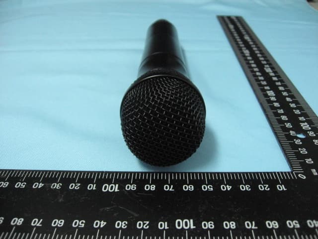
DLAS5HDX
Jul 30, 2014Wireless Microphone
Equipment Class
TBC - Licensed Broadcast Station Transmitter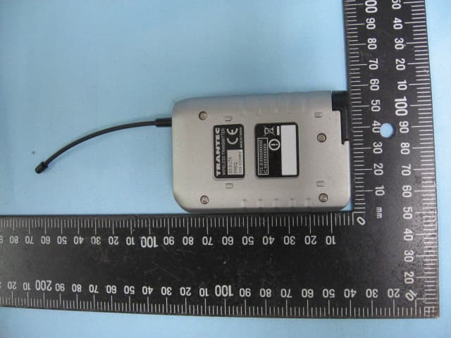
DLAS5LTX
Jul 30, 2014UHF Wireless Transmitter
Equipment Class
TBT - Licensed Broadcast Transmitter Worn on Body
DLAWM-5325
Jul 20, 2011Wireless Transmitter
Equipment Class
TBT - Licensed Broadcast Transmitter Worn on Body
DLAWM-5270B
Mar 29, 2011Wireless Microphone
Equipment Class
TNF - Licensed Non-Broadcast Transmitter Held to Face
DLAWM-5225
Mar 28, 2011Wireless Microphone
Equipment Class
TNF - Licensed Non-Broadcast Transmitter Held to Face