E9698109
Motorola Mobility LLC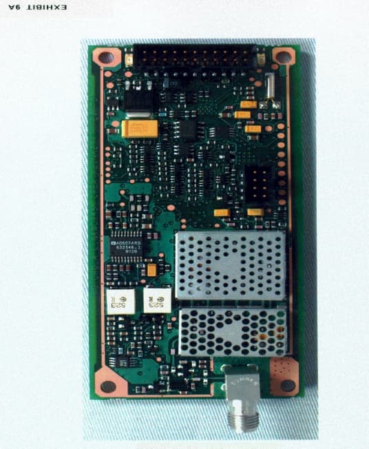
Click to zoom
Application Details
- Equipment Class
- PCB - PCS Licensed Transmitter
- Date of Grant
- Dec 20, 1998
- Application Purpose
- Original Equipment
- Date of Application
- Oct 25, 1998
- Frequency Range
- 896.00000000 - 901.00000000
- Company
- Motorola Mobility LLC
- Country
- United States
Documents & Files
Document Text
Text extracted from the exhibit documents filed with the FCC. Open a document above to read the original.
Users Manual
CreataLink 2 XT Installation and Operation Issue Date: October 15, 1998 68XXXXXXXX-O Series: Product Family 91B Data Transceiver TM CreataLink 2 XT Installation and Operation Issue Date: October 15, 1998 68XXXXXXXX-O Series: Product Family 91B Data Transceiver CreataLink 2 XT Data Transceiver Installation and Operation October 15, 199868XXXXXXXX-Oiii Foreword General Information The information in this manual has been reviewed for accuracy. However, no responsibility is assumed for inaccuracies. Motorola Inc. reserves the right to make changes to any products discussed herein. The information in this document is subject to change without notice. Motorola Inc. assumes no liability for hardware or software damage or loss of data because of errors or omissions in this manual. Motorola Inc. does not assume any liability arising from the application or use of any products or circuits described herein. Neither does Motorola Inc. convey any license under its patents or right of others. Refer questions concerning the contents of this manual to the following location: Motorola, Inc. Paging Products Group 3301 Quantum Boulevard, Boynton Beach, FL 33426 or telephone:1-800-MOT-FASD Refer questions regarding warranty repair to Motorola Paging Products Group: telephone:(888) 668-3273 Refer all other product inquiries to the One-Call-Support Center: telephone:(800) 520-7243 G05_FWD.FR5 Page iii Friday, October 23, 1998 1:53 PM ForewordCreataLink 2 XT Data Transceiver Installation and Operation iv68XXXXXXXX-OOctober 15, 1998 Computer Software Copyrights The Motorola products described in this manual might include copyrighted Motorola computer software stored in semiconductor memories and other media. Laws in the United States and other countries preserve for Motorola certain exclusive rights for copyrighted computer programs, including the exclusive right to copy or reproduce in any form the copyrighted computer software. Accordingly, any copyrighted Motorola computer software contained in the Motorola products described in this manual cannot be copied or reproduced in any manner without the express written permission of Motorola. Furthermore, the purchase of Motorola products does not grant, either directly or by implication, estoppel, or otherwise, any license under the copyrights, patents or patent applications of Motorola, except for the normal, nonexclusive, royalty-free license to use that arises by operation of law in the sale of a product. Trademarks CLP, CreataLink, FLEX, Motorola, the Motorola logo, and ReFLEX are trademarks or registered trademarks of Motorola, Inc. MAXIM is a registered trademark of MAXIM Integrated Products, Inc. Other trademarks are noted as such throughout this document. Trademarks contained herein are the acknowledged property of their respective owners. G05_FWD.FR5 Page iv Friday, October 23, 1998 1:53 PM CreataLink 2 XT Data Transceiver Installation and OperationForeword October 15, 199868XXXXXXXX-Ov Important Safety Information The installation, maintenance, and/or operation of this equipment may present potentially unsafe conditions, including, but not limited to, electrical shock, improper voltage to components, and improper operation that can cause personal injury, death or damage to property. Read Instructions: Read all the safety instructions before operating the equipment. Retain these safety instructions for future reference. Specialized procedures and instructions are required and must be followed. Also, all applicable safety procedures, such as Occupational, Safety, and Health Administration (OSHA) requirements, National Electric Code Requirements, local code requirements, safe working practices, and good judgement must be used by personnel. Heed Admonitions: Adhere to all warnings on the equipment and in the operating instructions. Follow all operating and use instructions. Two safety admonitions are used in this instruction manual to indicate: •Personal injury or equipment damage. •Harmful injury that may result in death. Mounting: Mount the equipment only as recommended by the manufacturer. Situate the equipment away from heat sources such as radiators, heat registers, stoves, or other equipment (including amplifiers) that produces heat. CAUTION This safety admonition applies to an operating or maintenance procedure, practice or condition which, if not strictly observed, could result in personal injury or damage to the equipment or database. DANGER This safety admonition applies to an operating or maintenance procedure, practice or condition which, if not strictly observed, could result in serious personal injury or death. G05_FWD.FR5 Page v Friday, October 23, 1998 1:53 PM ForewordCreataLink 2 XT Data Transceiver Installation and Operation vi68XXXXXXXX-OOctober 15, 1998 Power Sources and Grounding: Connect the equipment to the type of power source described in the installation instructions or as marked on the equipment. Take precautions to avoid defeating the grounding or polarization provisions of the equipment. Disconnect the power to the equipment by a circuit breaker when left unused for long periods of time. Cleaning:Clean the outside of the equipment by using only a damp cloth. Do not immerse the equipment in any type of liquid, including water. Do not use liquid cleaners or aerosol cleaners. Dirt or other foreign matter should not be allowed to accumulate in the interior of the enclosure. Damage Requiring Service: Do not attempt to perform service functions that are not described in the operating instructions. All other servicing should be referred to qualified service personnel. Motorola is not responsible for static damage to equipment not sold under the Motorola logo. Motorola, Inc. 1997, 1998. All rights reserved. Printed in the U.S.A. G05_FWD.FR5 Page vi Friday, October 23, 1998 1:53 PM CreataLink™2 XT Data Transceiver Installation and Operation / Chapter 1 1-168XXXXXXOctober 15, 1998 Introduction1 This chapter introduces the reader to this …
Text truncated - open the document above for the full version.
Cover Letter(s)
FCC ID:E9698109 DATE: 22 October 1998 TO: Authorization and Evaluation Division Federal Communications Commission Laboratory 7435 Oakland Mills Road Columbia, Maryland 21045 FROM: Scott Parker, Electrical Engineer SUBJECT: Request for Certification FCC ID: E9698109 Gentlemen: Motorola, Inc., 1500 Gateway Blvd., Boynton Beach, FL, 33426-8292, hereby requests certification for the CreataLink™2 XT transmitter models FCC ID: E9698109 as set forth in the Federal Communications Commission’s Rules and Regulations, Part 2 and 24. Model FCC ID: E9698109 is a Frequency Modulation Communications Transceiver having two frequency conversions and is designed for the reception of one fixed frequency within the range of 929 to 941 MHz and transmission in the range of 896 to 902 MHz. This radio equipment is intended for use in the common carrier paging system, PCS system, and SMR system. Exhibit 1 FCC ID:E9698109 FCC ID:E9698109 DATE: 22 October 1998 TO: Authorization and Evaluation Division Federal Communications Commission Laboratory 7435 Oakland Mills Road Columbia, Maryland 21045 FROM: William [Mac] Elliott, Staff Compliance Engineer SUBJECT: Request for Confidential Treatment FCC ID: E9698109 To the Commission: This is to request that the attached material associated with the application for the CreataLink™2 XT models FCC ID: E9698109 be withheld from public inspection and be treated confidentially. This request is made under the provisions of Section 0.457 (d) of the Commission’s Rules 47 C.F.R. 0.457 (d) (1997), and Section 552(b) (4) of the Freedom of information Act, 5 U.S.C. 552 (b)(4). The attached material , namely the schematics, is confidential commercial or business information that would not customarily be released to the public and that would not be apparent to the public from an examination of the equipment. Release of these materials to the public would cause the company substantial competitive harm. Under these circumstances, the information qualifies for confidential treatment under the FCC’s rules and the FOIA. The filing fee required with this request has been submitted with the payment for the approval fee. Should you have any questions concerning this matter, please call me at your earliest convenience. Regards, Mac Elliott Staff Compliance Engineer Motorola Inc. 561-739-3792 [email protected]
External Photos
FCC ID: E9698109 PHOTOGRAPHS Photograph Exhibit Number 1. Product Top View 9A 2. Product Bottom View 9B EXHIBIT 9 FCC ID: E9698109 EXHIBIT 9A FCC ID:E9698109 EXHIBIT 9B
Internal Photos
FCC ID: E9698109 PHOTOGRAPHS Photograph Exhibit Number 1. Product Top View 9A 2. Product Bottom View 9B EXHIBIT 9 FCC ID: E9698109 EXHIBIT 9A FCC ID:E9698109 EXHIBIT 9B
Operational Description
FCC ID:E9698109 GENERAL INFORMATION FCC Reference Pursuant 1. Production Plans 2.983 (c) Quantity production is planned. 2. Data Submittal Procedure Data is supplied in accordance with Part 2, Sub-part J of the Commissions rules. 3. Similar currently Type Accepted Transmitter, FCC ID: LX697FT4004. EXHIBIT 2 FCC ID:E9698109 DESCRIPTION 1. Transmitter Technical Characteristics – Pursuant 2.983 (d) A. RF Power Out 2 Watts B. Frequency Range Receiver 929-941 MHz Transmitter 896-902 MHz C. Frequency Stability 1 PPM D. Emissions 10KOFID E. Spurious Emissions -46 dBc F. DC Voltage and Current into the 4.5 Volts final RF Power Amplifier stage/stages 1.1 Amps Note: The following is the necessary bandwidth calculation. Personal Messaging Unit Specifications: Deviation = 2400 Hz maximum Maximum modulating frequency = 4800 symbols/2 symbols per cycle = 2400 Hz (Note: 9600 bits per second/2 bits per symbol = 4800 symbols per second) Bn = Necessary bandwidth, Hz M = Max modulating frequency, Hz D = Peak frequency deviation, Hz Bn = 2M + 2D = 2(2400) + 2(2400) = 9600 Hz 2. Transmitter Application This transmitter use is for the transmission of data only at 800, 1600, 6400, and 9600 bits per second to provide four level FSK modulation. A. Power Supplies CreataLink™2 XT is powered by an external 5 - 12 V DC power supply. The transmitter circuitry is powered from a 4.5 volt regulator and a 3.3 volt regulator. The receiver circuitry is powered from 4.5 volt regulator and a 3.3 volt regulator. The controller is powered from a 5 volt regulator and a 3.3 volt regulator. EXHIBIT 3 FCC ID:E9698109 DESCRIPTION – CONTINUED B. Antenna Available 1. Transmit No antenna will be supplied with CreataLink2 XT. An external antenna is connected to the personal messaging unit’s RF connector. Motorola’s optional external antenna meets e.r.p. limits. Integrators will be advised of e.r.p. limits imposed on them in selecting an antenna. 2. Receive No antenna will be supplied with theCreataLink2 XT. An external antenna is connected to the personal messaging unit’s RF connector. C. Squelch Types (not applicable) D. Microphone (not applicable) E. Maximum Transmit Channel Capability The product is capable of a maximum of 1023 transmit channels. F. Housing (not applicable - the transmitter is sold as a bare board with shielding.) G. Other Options 1. External Antenna Kit The external antenna kit consists of a low-profile monopole antenna with a radome and six feet of RG58/U coax with an RF connector. EXHIBIT 3 FCC ID: E9698109 CIRCUIT DESCRIPTION EXHIBIT 7 This section provides the description of circuits required by subpart 2.983 of the Commissions’ rules. The following are included: Circuit NameExhibit Number 1.Carrier Frequency Generation and Stabilization7A 2.Modulation Limiting7B 3.Means for Attenuating Spurious Emissions7C 4.Means for Limiting Power to Two Watts7D 5.Means for Limiting Impact of Externally Connected Signals7E FCC ID: E9698109 CIRCUIT DESCRIPTION – CARRIER FREQ. GENERATION & STABILIZATION EXHIBIT 7A 1. Carrier Frequency Generation and Stabilization Reference Oscillator and Fractional N Synthesizer The factors which have a direct impact on the frequency generating stability of the carrier are the stability of the reference oscillator, the ability of the charge pump to hold its voltage, and the phase lock loop’s ability to track out changes in the system while keeping the system phase-locked during operation. The reference oscillator used is a voltage-controlled 16.8 MHz quartz crystal (VCXO), which once locked to a forward channel is digitally compensated to guarantee that the output frequency variation is within 0.5PPM over the temperature range of -40 to +85C. Temperature compensation is performed by sending a digital word to an external voltage digital-to-analog converter (DAC), which adjusts the VCXO control voltage to adjust the frequency. The DAC has a tuning range of 0.1 to 3.5 VDC. This allows precise frequency adjustment using small linear steps. The adjustment range allows for a 60 PPM frequency shift. The charge pump voltage multiplier, which supplies the transmitter voltage controlled oscilla- tor (VCO) steering voltage, uses a buffered and divided sample of the 16.8 MHz VCXO signal from which the voltage multiplier diodes are clocked. This allows the demands of the control line voltage required to keep the loop locked to be met. The 16.8 MHz signal is also further divided to supply the reference frequency to the phase comparator, which in turn makes adjustments based on the phase difference of the reference frequency and the sampled VCO output frequency. All these circuits, along with the AFC (Automatic Frequency Control) algo- rithm, are tied back to the VCXO, allowing for 1 PPM frequency stability to be maintained. Transmit Voltage Controlled Oscillator The transmitter VCO consists of a buffer amplifier and a varactor-tuned tank circuit. The out- put impedance of the VCO is fixed with R742. This minimizes frequency shifting due to impedance changes at the output of the transmitter buffer and its corresponding input and out- put pads. The transmitter buffer also serves to isolate the VCO from the power supplies in order to minimize loading effects of the power amplifier on the VCO and thus maintain fre- quency stability. Exhibits 5C contain the schematics for the above described circuitry. CIRCUIT DIAGRAM Y700 reference oscillator U850 DAC output tuning voltage U720 synthesizer 16.8 MHz Q740 carrier feedback VCO 3 dB pad to PA U760 transmitter buffer FCC ID: E9698109 CIRCUIT DESCRIPTION – MODULATION LIMITING EXHIBIT 7B 2. Modulation Limiting The CreataLink2 XT has a modulation scheme which prevents overmodulation by utilizing a digital signal processor (DSP). The DSP controls the DC levels for FSK modulation while applying a digital splatter filter. The four DC levels are determined at the controller system level by measuring the frequency deviation level for each of the four symbol choices. Unique …
Text truncated - open the document above for the full version.
Parts List/Tune Up Info
FCC ID: E9698109 FUNCTION OF SEMICONDUCTORS AND OTHER ACTIVE DEVICES EXHIBIT 4 Transceiver Schematic Ref. DesignatorDevice TypeCircuit ApplicationSource Q740NPNreceive VCO #1Motorola Q780NPN/PNP ComboDC supply switchPhillips Q785PNPDC supply switchMotorola Q901NPNlow noise amplifierHewlett Packard Q930PNPDC biasMotorola Q931NPNlow noise amplifierMotorola Q935NPNBufferMotorola Q940NPNBufferMotorola Q980NPNreceive VCO #2Motorola U720BiCMOS ICTX/RX synthesizerMotorola U721CMOS ICOR gateToshiba U760silicon bipolar ICbuffer amplifierMotorola U770LDMOSRF power amplifierMotorola U771CMOS ICoperational amplifierNational Semiconductor U791CMOS ICoperational amplifierNational Semiconductor U850CMOS ICD/A convertorAnalog Devices U920GaAs ICRX mixerTriquint U930CMOS ICreceiver IF subsystemAnalog Devices U980CMOS ICRX synthesizerMotorola U981CMOS ICOR gateToshiba Y700VC TCXOreference oscillatorMotorola Y740Resonatorreceive VCO #1Murata FCC ID: E9698109 FUNCTIONOFSEMICONDUCTORSANDOTHERACTIVEDEVICES–CONTINUED EXHIBIT 4A Controller Schematic Ref. DesignatorDevice TypeCircuit ApplicationSource Q211P-channel FETopen collector I/OInternational Rectifier Q212P-channel FETopen collector I/OInternational Rectifier Q213Dual NPNopen collector I/OPhillips Q214Dual NPNopen collector I/OPhillips Q240PNPpower supplyRohm Q280P-channel FETbackup batteryMotorola Q281Dual NPNbackup batteryPhillips Q283NPN/PNP Combobackup batteryPhillips Q290NPN/PNP Comboopen collector I/OPhillips Q291Dual NPNopen collector I/OPhillips Q292NPN/PNP Comboopen collector I/OPhillips Q293NPN/PNP Comboopen collector I/OPhillips Q294Dual NPNopen collector I/OPhillips Q295NPN/PNP Comboopen collector I/OPhillips Q296NPN/PNP Comboopen collector I/OPhillips Q297Dual NPNopen collector I/OPhillips Q298NPN/PNP Comboopen collector I/OPhillips U100CMOS ICmicroprocessorMotorola U110CMOS ICdigital signal processorLucent U180CMOS ICA/D convertorAnalog Devices U190CMOS ICmemoryToshiba U210CMOS ICopen collector I/OMotorola U211CMOS ICopen collector I/OMotorola U220CMOS ICpower supplyNational Semiconductor U230CMOS ICpower supplySharp U240CMOS ICpower supplyRicoh U270CMOS ICRS-232Maxim U285CMOS ICbackup batterySharp U290CMOS ICOpen Collector I/OMotorola Y100Crystal38.4 KHz ClockMicro Crystal or Seiko FCC ID: E9698109 TUNE-UP PROCEDURE EXHIBIT 6 The following tune-up procedure is similar to what will appear in the final service manual. Only qualified service shops will have the equipment necessary to make transmitter adjustments (fre- quency and modulation parameters) via Tune Modes. Recommended Tune/Test Equipment Intel-based PC running Windows98 operating system (also called “PC”) CreataLink™ Paging Programming Software for the PC (also called “PPS software”) Serial Interface cable (for power and a serial connection between CreataLink™ and the PC) HP53310A Modulation Domain Analyzer with options 031 and 001 (also called “MDA”) HP8991A Peak Power Analyzer HP84815A Peak Power Sensor HP53131A Universal Counter Signal/oscilloscope probe (for attachment to HP53131A) 20 dB attenuator 10 MHz reference line Test Mode Descriptions Typically, the radio is tested in Test Mode first to verify proper radiated performance (FM deviation, silent carrier, etc., all at 901.40625 MHz test frequency). If any parameter needs tuning, the radio is placed in Tune Mode using the PPS software, which reads and writes to the radio via the serial interface cable. Once the parameter is tuned, the radio is tested to verify the correct tuned value. The applicable test modes are: Test Mode List For Transmitter Tune-Up (TX at 901.40625 MHz) Test ModeRadio Output Reference Oscillator Test16.8 MHz signal at Test Point TP700 Silent Carrier Testconstant tx: unmodulated carrier Balance Low Testconstant tx: 100 Hz sinewave at full deviation Balance High Testconstant tx 1600 Hz sinewave at full deviation Symbol Deviation Testconstant tx: pseudo-random four-level FSK data sequence Transmitter On16 msec tx repeated every 2 sec: simulated ack data Long Reverse550 msec tx repeated every 2 sec: four-level stair-step data FCC ID: E9698109 TUNE-UP PROCEDURE – CONTINUED EXHIBIT 6 How to Place Radio in Tune Mode 1. Plug the serial interface cable into a wall outlet, then connect it to the PC serial port and to the radio. 2. On the PPS software, click theRead Device icon to read the radio’s current tuning values. (Note: The radio must be read by the PPS software successfully before any other opera- tions can be performed.) 3. Click on theDevice Tuning icon. This will bring up the Tuning Toolbar icons. 4. Click on the desired test mode icon. This will create a secondary window showing the cur- rent tuning values. Only the tuning values that correspond to the test mode are able to be adjusted. 5. Click on theStart Testbutton. The test mode will now be active; adjust the tuning value as needed. 6. When tuned, the test mode is stopped by selecting theStop Test button. 7. If any tuning values were adjusted, then click on theAcceptbutton to accept the new tuning values. Then click on theWrite Device icon to write the new tuning values to the radio. Adjust the Reference Oscillator 1. Connect the 10 MHz reference line and signal probe to the HP53131A Universal Counter. 2. Connect the signal probe to TP700 on the transceiver board. 3. Initiate the Reference Oscillator tune mode by clicking theReference Oscillator Testicon on the PPS software and then click on theStart Test button. 4. Measure and verify that the reference oscillator is outputting 16.8 MHz at TP700. 5. If the reference oscillator is not outputting within 0.1 ppm of 16.8 MHz at TP700, tune the oscillator as necessary using the PPS software until it meets this tolerance level. 6. Click on theStop Test button to disable the test. 7. Write the final tuned value to the radio by clicking theAccept button and then click on the Write Device icon. FCC ID: E9698109 TUNE-UP PROCEDURE – CONTINUED EXHIBIT 6 Adjust the Silent Carrier Frequency/Verify Carrier Noise …
Text truncated - open the document above for the full version.
Test Report
SUBMITTED MEASURED DATA MeasurementExhibit 1.Index8 2.RF Power Out8A 3.Modulation Characteristics a. Baseband Splatter Filter Response8B b. Baseband Filtered Data8C c. Demodulated RF Data (Deviation)8D 4. Occupied Bandwidth A. NBPCS Emission Limits8E B. SMR Emission Limits8F 5.Spurious Emissions at Antenna Terminals A. Carrier Frequency at +/-50 kHz8G B. Carrier Frequency at +/- 25 kHz8H C. 9 kHz to 10 GHz8I 5. Transmitter Radiated Spurious A. Vertical Polarization8J B. Horizontal Polarization8K 6.Frequency Stability a. Frequency Stability vs. Temperature8L b. Frequency Stability vs. Supply Voltage8M EXHIBIT 8 FCC ID: E9698109 MEASUREMENT PROCEDURE AND TEST EQUIPMENT USED EXHIBIT 11 Except where otherwise stated, all measurements are made following the Telecommunications Industry Standard (TIA) / Electronics Industries Association (EIA) Minimum Standard for Land Mobile FM or PM Communications Equipment Measurement and Performance Standards (TIA/ EIA-603). This exhibit presents a brief summary of how the measurements were made, the required limits, and the test equipment used. The following procedures are presented with this application. DescriptionExhibit Number ___ 1. RF Power Output_ X_11A ___ 2. Occupied Bandwidth_ X_11B ___ 3. Spurious Emissions at Antenna Terminals_ X_11C ___ 4. Transmitter Radiated Spurious Emissions_ X_11D ___ 5. Frequency Stability_ X_11E ___ 6. Test Equipment List_ X_11F FCC ID: E9698109 MEASUREMENT PROCEDURE – RF POWER OUTPUT EXHIBIT 11A RF Power Output - Pursuant to FCC Rules 2.985 Method of Measurement The radiated RF power output is measured with the transmitter adjusted in accordance with the tune-up procedure to give the value of voltage and current specified in Exhibit 3 as required by 2.983(d)5. The 20 dB attenuator and cable losses are measured using a network analyzer and calibrated out of the measurement. The 20 dB attenuator is connected to the unit’s RF connector to supply a good 50 ohm load for the transmitter. The attenuator is then connected to an HP 8991A Peak Power Analyzer, via an HP 84815A Peak Power Sensor. The unit is placed into Tranmitter On test mode. The ampitude of the RF power out is measured on the peak power analyzer. FCC ID: E9698109 MEASUREMENT PROCEDURE – OCCUPIED BANDWIDTH EXHIBIT 11B Occupied Bandwidth - Pursuant to FCC Rules 2.989 Method of Measurement Data on occupied bandwidth is presented in the form of a spectrum analyzer plot which illustrates the transmitter sidebands. A plot is taken of the unmodulated carrier for reference, to which is superimposed the sideband trace generated by modulating the carrier with a pseudo-random four level signal. The DSP (U110) is used to generate the pseudo-random signal. This signal is digi- tally filtered internally in the DSP. The output of the splatter filter is then fed into the modulation input port of the fractional N synthesizer (U720). The RF output of the transmitter is then con- nected to the Hewlett Packard HP8560A Spectrum Analyzer through a Narda 20 dB attenuator. The HP8560A Spectrum Analyzer’s settings were as follows: detector on Positive Peak, resolu- tion bandwidth on 300 Hz, video bandwidth on 300 Hz, sweep on automatic, span on 50 KHz. The occupied bandwith was measured by making multiple sweeps with the trace on Maximum Hold until the frequency spectrum ceased to change. FCC Limits – Per Applicable Rule Parts Measured Data: On any frequency outside the authorized bandwidth and removed from the edge of the authorized bandwidth by a displacement frequency (Fd in kHz) of up to and including 20 kHz: at least, or, or 70 dB, whichever is the lesser attenuation. For any frequency outside the authorized bandwidth and removed from the edge of the authorized bandwidth by a displacement frequency (Fd in kHz) of more than 20 kHz: at least or 80 dB, whichever is the lesser attenuation. Power is speci- fied in Watts. 116 Fd5+() 3.05 -------------------- dB 10 log5010Power()dB 10 log+ 4310Power()dB 10 log+ FCC ID: E9698109 MEASUREMENTPROCEDURE–SPURIOUSEMISSIONSATANTENNATERMINAL EXHIBIT 11C Spurious Emissions at Antenna Terminals - Pursuant to FCC Rules 2.991 Method of Measurement Data on the spurious emissions at the antenna terminals is presented in the form of spectrum ana- lyzer plots which illustrates the magnitude of spurious frequencies. A Narda 20 dB attenuator is connected to the RF connector to provide the suitable antenna load. Then the 20 dB attenuator is connected to the Hewlett Packard HP8596E Spectrum Analyzer and measurements are made using the transmit carrier frequency. FCC Limits – Per Applicable Rule Parts Spurious emissions at the antenna terminals shall be attenuated below the maximum level of emission of the carrier frequency in accordance with the following formula: Spurious Attenuation =. Power is specified in Watts.4310Power()dB 10 log+ FCC ID: E9698109 MEASUREMENT PROCEDURE – TX SPURIOUS EMISSIONS EXHIBIT 11D Radiated Spurious Emissions - Pursuant to FCC Rules 2.993 Test Site The test site is located in Boynton Beach, Florida, which is reasonably free from RF interference. The equipment is placed on the turntable and connected to the intended power source. The mea- surement is performed with the optional external antenna as the radiating element. A horn antenna located thirty (30) meters away from the transmitter picks up any signal radiated from the trans- mitter. A spectrum analyzer covering the necessary frequency range is used to detect and measure any radiation picked up by the antenna. Method of Measurement The testing procedure is repeated for both horizontal and vertical polarizations of the receiving antenna. Relative signal strength is indicated on the spectrum analyzer connected to this antenna. Actual radiated signal strength for each spurious and harmonic frequency observed is correlated to a standard signal generator with a calibrated out connected to a horn quadridge antenna and with its frequency adjusted to the particular discrete frequency…
Text truncated - open the document above for the full version.
Contact Information
Applicant
Charles L Eger(Senior Director, Global Regulatory and Issue Mgmt)
Technical Contact
SAME AS ITEM 4
561-739-3792
Non-Technical Contact
SAME AS ITEM 4
561-739-3792
Technical Specifications
| # | Rule Parts | Frequency Range | Power Output | Emission | Tolerance |
|---|---|---|---|---|---|
| 2 | 9 | 896 MHz - 901 MHz | 2 W | 10K0F1D | 1 ppm |
Other Applications from Motorola Mobility LLC
E9601110
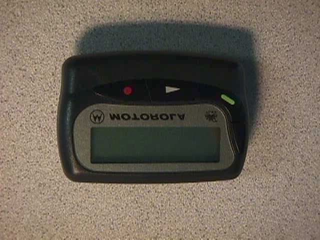
Feb 13, 2001Motorola Scriptor Jazz 200
Equipment Class
CXX - Communications Rcvr for use w/ licensed Tx and CBs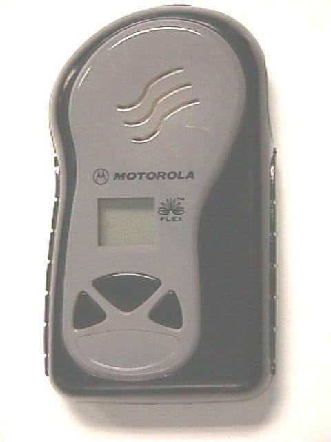
E9698108
Jan 05, 1999Transceiver
Equipment Class
PCT - PCS Licensed Transmitter worn on body
E9698107
Aug 06, 1998Paging Receiver
Equipment Class
CXX - Communications Rcvr for use w/ licensed Tx and CBsE9698105
May 27, 1998Paging Receiver
Equipment Class
CXX - Communications Rcvr for use w/ licensed Tx and CBsE9698102
Mar 24, 1998CXX - Communications Rcvr for use w/ licensed Tx and CBs
Equipment Class
CXX - Communications Rcvr for use w/ licensed Tx and CBs