ED9LMX9820ASMBluetooth Serial Port Module
Texas Instruments Inc.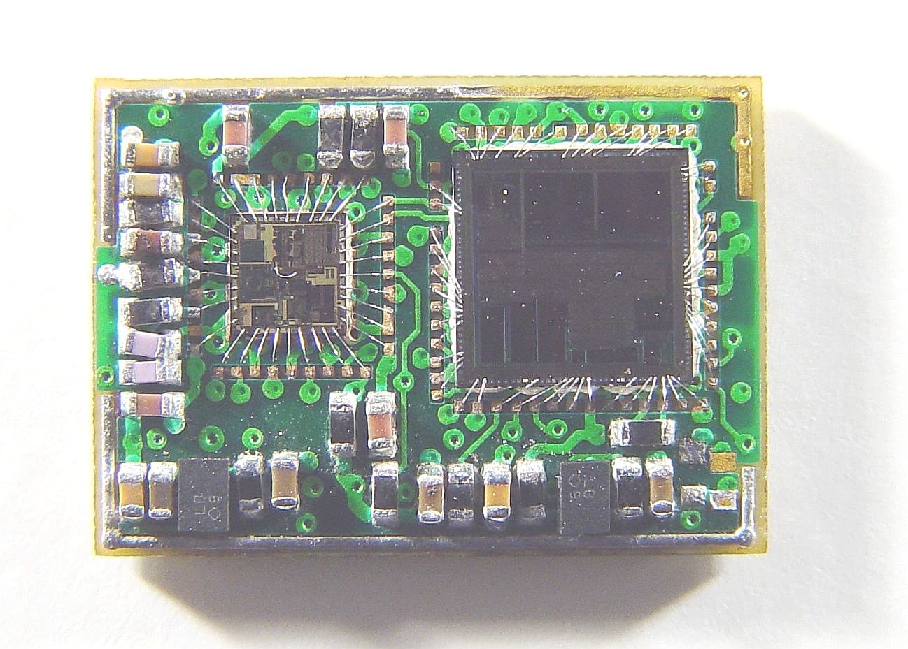
Click to zoom
Application Details
- Equipment Class
- DSS - Part 15 Spread Spectrum Transmitter
- Date of Grant
- Oct 04, 2005
- Application Purpose
- Original Equipment
- Date of Application
- Oct 04, 2005
- Equipment Note
- Bluetooth Serial Port Module
- Frequency Range
- 2402.00000000 - 2480.00000000
- Company
- Texas Instruments Inc.
- Country
- United States
Documents & Files
Document Text
Text extracted from the exhibit documents filed with the FCC. Open a document above to read the original.
Users Manual
LMX9820A Bluetooth TM Serial Port Module Introduction The purpose of this manual is to explain correct way how to integrate module LMX9820A to the end product. It includes procedures that shall assist you to avoid unforeseen problems. This manual presents information that shows how module and OEM product, where module integrated, complies with regulations in certain regions. Any modifications, not expressly approved by the manufacture could void the authority to operate in these regions. Content 1. General 2. Module design application 3. Regulatory Compliance. 4. FCC Regulatory Information 4.1 Labelling 4.2 Antenna implementation notes. 4.3 Other regulatory notes for OEM 5. A separate approval. 1.General This Bluetooth Serial Port Module has to be installed and used in accordance with the technical description/installation instructions provided by the manufacturer. This Bluetooth Serial Port Module is intent to be placed on the market in all States, where the Bluetooth technology and the used frequency band is released. For detail information concerning type approval of this module (eg. Where this module is already pre-approved) please contact the authorized local distributor or the manufacture. The system may only be implemented in the configuration that was authorized. Note that any changes or modifications to this equipment not expressly approved by that manufacture could void the user’s authority to operate this equipment. 2.Module design application 2.1 Model Number LMX9820A 2.2 Features and Specifications 1) Bluetooth Version 1.1 Qualified. 2) Temperature Range: -40C to +85C 3) Small form factor (10.1mm x 14mm x 1.9mm) 4) Implemented in CMOS technology on FR4 Substrate 5) Operating Frequency Band: 2.402GHz to 2.480GHz 6) Sensitivity: -80dBm typical 7) Output Power: +4dBm maximum (measured at RFinout of LMX5452 micro module) 8) Operating Temperature: –40 to 85 degree C 9) Storage Temperature: -60 to 150 degree C 10) Operating Voltage: VCC 2.85V ~ 3.6V 11) Power Consumption: TX burst (peak) is 50mA max RX burst (peak) is 40mA max 12) Data rate: Asynchronous: 723kbp/57.6kbps Synchronous: 433.9kbps/433.9kbps 2.3 Applications area. PDA, POS Terminals, Data Logging Systems, Audio Gateway applications, other application. 2.4 Terminal Functions Table-1 Table-2 Table-3 Table-4 Table-5 Table-6 Table-7 2.5 Software Stack for module and customer side example 3. Declaration about the performed tests. The National Semiconductor module LMX9820A is wireless data transmission system. This “Bluetooth” module can be integrated into various end products. National Semiconductor declares that The LMX9820A complies to Part 15 of the FCC Rules. 4. FCC regulatory Information. The Federal Communication Commission Radio Frequency Interference Statement includes the following paragraph: This equipment has been tested and found to comply with the limits pursuant to Part 15 of the FCC Rules. These limits are designed to provide reasonable protection against harmful interference in a residential installation. This equipment generates, uses and radiates radio frequency energy and, if not installed and used in accordance with the instructions, may cause harmful interference to radio communication. However, there is no guarantee that interference will not occur in a particular installation. If this equipment does cause harmful interference to radio or television reception, which can be determined by turning the equipment off and on, the user is encouraged to try to correct the interference by one or more of the following measures: -Reorient or relocate the receiving antenna. -Increase the separation between the equipment and receiver. -Connect the equipment into an outlet on a circuit different from that to which the receiver is connected. -Consult the dealer or an experienced radio/TV technician for help. Changes or modifications not expressly approved by the party responsible for compliance could void the user's authority to operate the equipment. 4.1 Labeling. The FCC ID will be placed on top of the product as shown below: End-products into which the RF module will be installed must wear the auxiliary label ("Contains FCC ID: XXXXYYYY" or "Contains Transmitter Module LMX9820A FCC ID ED9LMX9820ASM" When end-product into which RF module is integrated exceeds size of a PCMCIA card (approx. 8 x 10 cm) than the FCC Statement must be placed onto the device: ******************************************************************* This device complies with Part 15 of the FCC Rules. Operation is subject to the following two conditions: (1) this device may not cause harmful interference, and (2) this device must accept any interference received, including interference that may cause undesired operation. *************************************************************** The physical size of the label and font size of the lettering will be dependant on the size of the final product, but in any case will always be clearly visible to all persons exposed to the transmitter. Otherwise this statement can be placed into the users manual of the end-product. 4.2 Antenna implementation notes. This transmitter was tested and FCC approved for antenna with maximum gain 0 dBi. Recommended external antennas are described as following. Manufacture SN Gain Frequency Range Temp. Fractus FR05-S1-N-0-104 0dBi 2400~2500MHz -40C~85C WPI WPSMLANT001A 0dBi 2400~2500MHz -40C~85C Murata ANCW12G45SAA110TT1 0dBi 2400~2500MHz -40C~85C 4.3 Other regulatory notes for OEM. Modular transmitters save manufacturers the time and any related expenses that would be incurred if a new equipment authorization were needed for the same transmitter when it is installed in a new device. This means that it can be integrated into end products without further testing or approval listing. The manufacturer must state the National Semiconductors part number and product reference in his literature in order to meet the requirements of the Bluetooth and regulatory. This shoul…
Text truncated - open the document above for the full version.
Cover Letter(s)
Power of attorney for 7layers Commercial Power of Attorney for the type approval / registration of the LMX9820A in several countries. The company 7layers, D-40880 Ratingen, has been contracted by National Semiconductor Corp. to obtain “Modular Radio Type Approvals” for the following electronic components, manufactured and/or released by National Semiconductor Corp.: LMX9820A Unless future correspondence from National Semiconductor Corp. directs otherwise, please extend your full cooperation to 7layers regarding matters to the above mentioned products for the period beginning 09-29-05 through 10-31-05. Thank you Peter Zhang Senior Application Engineer, National Semiconductor Corp. DCD Group 10105 Pacific Heights Blvd, San Diego 09-29-05
Cover Letter(s)
CONFIDENTIALITY REQUEST1.jpg (JPEG Image, 1700x2339 pixels)file://///Alpha01/4_MS5/PROJECTS/2004/4_Natsc_IRV_0104_BTT/TAS/_FCC_phoenix_L_%20ap...
Cover Letter(s)
4_Natsc_IRV_0104_BTT FCC Federal Communications Commission Aleksey Yevdokymov 20 April 2005 Phone +49 (0) 2102 749 387 Fax +49 (0) 2102 749 350 Email: [email protected] Request for the modular approval - FCC ID: ED9 LMX9820ASM Dear Application Examiner, the Bluetooth module LMX9820A is seeking for FCC authorization as a modular transmitter. There is no reference oscillator and antenna installed on the module. DA 00-1407 require, that a transmitter module is defined as a complete RF transmitter, so that it must contain its own reference oscillator. In this particular case no own reference oscillator is on board, this leads to a "Limited Modular Approval" The following requirements are fulfilled: 1. The modular transmitter must have its own RF shielding The radio portion of the module is contained in its own RF shielding. See enclosed product photos in exhibit “L_External photo_LMX9820A”. 2. The modular transmitter must have buffered modulation/data inputs The module has a memory management unit inside of the IC. It buffers the data inputs from UART and USB terminal. 3. The modular transmitter must have its own power supply regulation The IC contains an own voltage regulation. In case of changes in the supply voltage VCC (for example caused by temperature changes or other effects), the internal voltage will be stabilized. 4. The modular transmitter must comply with the antenna requirements of Section 15.203 and 15.204c The transmitter shall only be used with the tested integral antenna or with an antenna that has less antenna gain. Requirements for the use of external antennas Registergericht h registered in:Vorstand h Board of Directors:7 layers AG, Borsigstrasse 11 Ratingen, HRB 3264Dr. Wolfgang Dahm40880 Ratingen, Germany Aufsichtsratsvorsitzende h Dr. Hans-Jürgen MeckelburgPhone: +49 (0) 2102 749 0 Chairman of the Supervisory Board:Fax: +49 (0) 2102 749 350 Dr. Sabine Grobeckerwww.7Layers.com - 2 - are specified in Antenna design Exhibit “I_antenna_LMX5251_2_LMX9814_20 AN” and “ User manual” 5. The modular transmitter must be tested in a stand-alone configuration The EUT was tested in a stand-alone configuration. The module was fixed in Development Kit during the test. See also test setup photos and test report (B_4_Natsc_IRV_0104_BTT_FCCa). For radiated measurements, the required distance of 10 cm was ensured by special connector. 6. The modular transmitter must be labelled with its own FCC ID number The labelling information was specified in Exhibit D_label_linforomation. If the module is installed inside of an end-product, OEM customer will be instructed to how to apply the exterior label. Relevant OEM labelling requirements present in the product user manual. 7. The modular transmitter comply with any specific rule or operating requirements applicable to the transmitter and the manufacturer must provide adequate instructions along with the module to explain any such requirements. The EUT is compliant with all applicable FCC rules. Detail instructions are given in the product Users Guide 8. The modular transmitter must comply with any applicable RF exposure requirements. The maximum measured power output is 1,629 mW (2,12 dBm), the maximum antenna gain is 0 dBi = numeric gain 1 (see also FCC test report - Exhibit Test report FCC Part 15.247 B_4_Natsc_IRV_0104_BTT_FCCa) The maximum measured power output is 1.63mW (2.12 dBm), the maximum antenna gain is 0 dBi which is far below the low threshold defined as (60/f GHz) mW for d < 2.5 cm in the TCB exclusion list. For these devices no action is required. Please contact us if you have any additional questions. Best Regards 7layers AG
External Photos
LMX9820A interanal photo LMX9820A External photo top bottom M odule labelled as evaluation engineering sample. FCC labelling information present as separate document
ID Label/Location Info
FCC labelling declaration.jpg (JPEG Image, 1700x2339 pixels)file:///C:/Dokumente%20und%20Einstellungen/YevdAle.7LRATDE/Lokale%20Einstellungen/Temp...
Internal Photos
LMX9820A interanal photo LMX9820A External photo top bottom M odule labelled as evaluation engineering sample. FCC labelling information present as separate document
Operational Description
Bluetooth is a registered trademark of Bluetooth SIG, Inc. and is used under license by National Semiconductor. ©2005 National Semiconductor Corporation National Semiconductor Application Note Antenna Design for LMX5251, LMX5252, LMX 9814, and LMX9820 Antenna Design for LMX5251, LMX5252, LMX9814, and LMX9820 1.0 Introduction This application note is intended for designers using the LMX5251 or LMX5252 Bluetooth ® radio chips or LMX9814 or LMX9820 Bluetooth modules. Antenna design for various applications is described along with theory, matching circuit description, suppliers and examples. Any structure that is resonant at 2.45 GHz with bandwidth more than 100 MHz and efficiency >50% can be considered a Bluetooth antenna. Therefore, a countless variety of antennas can be used, and they are application-specific. Some common types are: Wire Monopole—This consists of a simple wire soldered at one end from which it is fed against a ground plane. It is trimmed to be resonant at 2.45 GHz and provides good performance and high efficiency. The disadvantage of this antenna is that it is not low profile because it projects above the PCB. PIFA—The Printed Inverted F Antenna is like a monopole printed on a PCB, but it has a ground point and feed point along the main resonant structure. Helix—Similar to the wire monopole, except that it is coiled around a central core (usually air) making the physical dimensions smaller. It provides excellent perfor- mance, but projects above the PCB. Ceramic—Surface mount dielectric antennas are the smallest types of antennas available, because they are printed on a high-dk ceramic slab, which makes the elec - tric field concentrated allowing the antenna to be made small while keeping a high resonant frequency. This application note only describes PIFA and ceramic antennas because they are the most common, low-profile, smallest, and inexpensive types available. 2.0 Theory Printed and surface-mount antennas have certain common properties. Area around and beneath the radiating element must be kept copper-free. The ground plane must be placed on one side of the radiating element. Bandwidth is >100 MHz with VSWR <2.5 and efficiency >60%. The antenna will detune if any object is placed close to it (in its near field). This has an effect of pulling the frequency, which must be retuned to 2.45 GHz. An oscillating or constantly accelerating charge is critical in producing propagating waves. A static or non-accelerating charge will result in a non-propagating electric field. But this is not the only condition for radiation. For example, consider a printed λg/4 element on microstrip, as shown in Figure 1. Figure 1. Fringing Field With Full Ground Plane The fringing field around the microstrip due to the ground plane directly underneath the substrate will be confined to a small area. If a network analyzer is connected to the feed point, it would indicate a high VSWR and narrow bandwidth. This means very little radiation is being emitted from the microstrip element. Quarter Wave Substrate Fringing field around Microstrip Feed Ground MARCH 2005 www.national.com2 To increase the radiation emission and achieve greater bandwidth, the ground plane must be moved away from the microstrip element which makes the fringing field cover more distance, as shown in Figure 2. But it should be noted that if the ground plane is moved too far, then the fringing field stops altogether, and there is no radiation. Therefore, the position and size of the ground plane is vital in the design of a good radiator. Figure 2. Fringing Field With Partial Ground Plane The antenna could be imagined as an impedance trans- former, transforming the impedance of a microstrip line (50Ω) to that of free space (377Ω), which allows the power to be transferred from a guided wave to a free-space wave. The radiation pattern from such antennas in which the physical size is much smaller then wavelength (L << λ) is almost symmetrical in all directions, as shown in Figure 3. The pattern can be controlled only when L is similar or greater than λ. Figure 3. Antenna Radiation Pattern Input return loss when viewed on a network analyzer looks like that shown in Figure 4, with the full band covered with VSWR < 2. This gives very good matching into the antenna, however in real conditions when the antenna is detuned due to handling or placement of components close to it, a VSWR of 3 to 4 is typical. Figure 4. Return Loss Quarter Wave Radiation Feed Azumith Cut 5 -5 -15 0 180 90 120 60 30 150 270 300 240 210 330 -35 -25 Elevation Cut 5 -5 -15 0 180 90 120 60 30 150 270 300 240 210 330 -35 -25 5 4 3 2.22.32.4 Freq. (GHz) 2.52.62.7 2 VSWR 1 6 3 www.national.com 3.0 Layout 3.1 PIFA ANTENNA The typical length of a 2.45-GHz resonant printed antenna is 20 to 25 mm, depending on the thickness of the sub - strate and dielectric constant. Copper clearance is required around the radiating element which is fed from a point along it, as shown in Figure 5. The position of the feed can be used to control the input impedance into the antenna. The ground plane required on one side of the antenna is approximately 20 mm wide. If it were any smaller, it will start to reduce the bandwidth at the input. Good design practice is to have a three-element matching network going into the feed, to give some additional tuning ability if required. To obtain the exact dimensions of the design, input impedance and bandwidth would have to be simu - lated over the frequency band using an antenna simulation package. Alternatively an antenna manufacturer can be contacted that has the capability to make such a design. Figure 5. Printed Inverted-F Antenna (PIFA) The PIFA is placed on the edge of the motherboard PCB, as shown in Figure 6. The area around the corner is kept copper-free, and any components such as the shielding that come close to the PIFA may pull its frequency. This can be retuned by milling the end of the radiating element. The LMX5251/LMX5252 and its …
Text truncated - open the document above for the full version.
Test Report
7 layers AG, Borsigstrasse 11 40880 Ratingen, Germany Phone: +49 (0) 2102 749 0 Fax: +49 (0) 2102 749 350 http://www.7Layers.com Aufsichtsratsvorsitzende Chairman of the Supervisory Board: Michael Abels Vorstand - Board of Directors: Dr. Hans-Jürgen Meckelburg Registergericht - registered in: Düsseldorf, HRB 44096 USt-IdNr VAT Nr: DE 203159652 InterLab is a registered trademark of 7 layers AG FCC Measurement/Technical Report on Bluetooth ® transceiver LMX9820A Report Reference: 4_Natsc_IRV_0104_BTT_FCCa Test Laboratory: 7 layers AG Borsigstrasse 11 40880 Ratingen Germany email: [email protected] TTI-P-G 178/99 Note: The following test results relate only to the devices specified in this document. This report shall not be reproduced in parts without the written approval of the testing laboratory. Testreport Reference: 4_Natsc_IRV_0104_BTT_FCCa Page 2 of 51 Table of Contents 0 Summary....................................................................................................3 0.1 Technical Report Summary......................................................................3 0.2 Measurement Summary..........................................................................4 1 Administrative Data.......................................................................................6 1.1 Testing Laboratory.................................................................................6 1.2 Project Data.........................................................................................6 1.3 Applicant Data......................................................................................6 1.4 Manufacturer Data.................................................................................6 2 Product labeling............................................................................................7 2.1 FCC ID label.........................................................................................7 2.2 Location of the label on the EUT...............................................................7 3 Test object Data...........................................................................................8 3.1 General EUT Description.........................................................................8 3.2 EUT Main components............................................................................9 3.3 Ancillary Equipment...............................................................................9 3.4 EUT Setups...........................................................................................9 3.5 Operating Modes...................................................................................9 4 Test Results...............................................................................................10 4.1 Occupied bandwidth.............................................................................10 4.2 Peak power output...............................................................................12 4.3 Spurious RF conducted emissions...........................................................14 4.4 Spurious radiated emissions..................................................................16 4.5 Band edge compliance..........................................................................20 4.6 Dwell time..........................................................................................22 4.7 Channel separation..............................................................................24 4.8 Number of hopping frequencies..............................................................25 5 Test Equipment..........................................................................................26 6 Photo Report..............................................................................................29 7 Setup Drawings..........................................................................................33 8 Annex.......................................................................................................34 Testreport Reference: 4_Natsc_IRV_0104_BTT_FCCa Page 3 of 51 0 Summary 0.1 Technical Report Summary Type of Authorization Certification for an Intentional Radiator (Frequency Hopping Spread Spectrum). Applicable FCC Rules Prepared in accordance with the requirements of FCC Rules and Regulations as listed in 47 CFR Ch.1 Parts 2 (2001-10-01 Edition) and 15 (2004-07-12 Edition). The following subparts are applicable to the results in this test report. Part 2, Subpart J - Equipment Authorization Procedures, Certification Part 15, Subpart C – Intentional Radiators § 15.201 Equipment authorization requirement § 15.207 Conducted limits § 15.209 Radiated emission limits; general requirements § 15.247 Operation within the bands 902-928 MHz, 2400-2483,5 MHz and 5725-5850 MHz Note: The tests were selected and performed with reference to the FCC Public Notice DA 00- 705, released March 30, 2000 Instead of applying ANSI C63.4-1992 which is referenced in the FCC Public Note, the newer ANSI C63.4-2003 is applied. Summary Test Results: The EUT complied with all performed tests as listed in chapter 0.2 Measurement Summary. Testreport Reference: 4_Natsc_IRV_0104_BTT_FCCa Page 4 of 51 0.2 Measurement Summary FCC Part 15, Subpart C § 15.207 Conducted emissions (AC power line) Not applicable because the EUT is not powered by AC Mains. FCC Part 15, Subpart C § 15.247 (a) (1) (ii) Occupied bandwidth The measurement was performed according to FCC § 15.31 2004 OP-Mode Setup Port Final Result op-mode 1 4E040b01 temp. ant. conn. passed op-mode 2 4E040b01 temp. ant. conn. passed op-mode 3 4E040b01 temp. ant. conn. passed FCC Part 15, Subpart C § 15.247 (b) (1) Peak power output The measurement was performed according to FCC § 15.31 2004 OP-Mode Setup Port Final Result op-mode 1 4E040b01 temp. ant. conn. passed op-mode 2 4E040b01 temp. ant. conn. passed op-mode 3 4E040b01 temp. ant. conn. passed FCC Part 15, Subpart C § 15.247 (d) Spurious RF conducted …
Text truncated - open the document above for the full version.
Test Report
Supplement I to Test Report: 4_Natsc_IRV_0104_BTT_FCCa Band edge compliance Date: 2005-09-06 Supplement I to Test Report: 4_Natsc_IRV_0104_BTT_FCCa Page 2 of 2 1 Band edge compliance radiated operating mode 3 Op. Mode higher band edge op-mode 3 TX on 2480 MHz Radiated measurement 10 20 30 40 50 60 70 80 Level [dBμV/m] 2.48G 2.485G 2.49G 2.495G 2.5G Frequency [Hz] Marker: 2.4835 GHz 46.47 dBμV/m Delta Mk: 0 Hz -11.6 dB MES Nat_0104_02_pre PK MES Nat_0104_02_pre AV LIM FCC 15.209 3m Field Strength QP/AV Limit LIM FCC 15.209 3m Peak Field Strength Peak Limit
Test Report
Registergerichth registered in:Vorstandh Board of Directors:7 layers AG, Borsigstrasse 11 Ratingen HRB 3264Dr. Wolfgang Dahm40880 Ratingen, Germany AufsichtsratsvorsitzendehDr. Hans-Jürgen MeckelburgPhone: +49 (0) 2102 749 0 Chairman of the Supervisory Board:Fax: +49 (0) 2102 749 350 Dr. Sabine Grobeckerwww.7layers.com Annex Additional declaration part according FCC 15.247 for Bluetooth TM Devices Version: 2002-06-01 Annex - Additional declaration part according FCC 15.247 for Bluetooth devices Page 2 of 5 pages 1 Output power and channel separation of a Bluetooth device in the different operating modes: The different operating modes (data-mode, acquisition-mode) of a Bluetooth device don’t influence the output power and the channel spacing. There is only one transmitter which is driven by identical input parameters concerning these two parameters. Only a different hopping sequence will be used. For this reason the check of these RF parameters in one op-mode is sufficient. 2 Frequency range of a Bluetooth device: Hereby we declare that the maximum frequency of this device is: 2402 – 2480 MHz. This is according the Bluetooth Core Specification (+ critical errata) for devices which will be operated in the USA. This was checked during the Bluetooth Qualification tests (Test Case: TRM/CA/04-E). Other frequency ranges ( e.g. for Spain, France, Japan) which are allowed according the Core Specification are not supported by this device. 3 Co-ordination of the hopping sequence in data mode to avoid simultaneous occupancy by multiple transmitters: Bluetooth units which want to communicate with other units must be organised in a structure called piconet. This piconet consist of max. 8 Bluetooth units. One unit is the master the other seven are the slaves. The master co-ordinates frequency occupation in this piconet for all units. As the master hop sequence is derived from its BD address which is unique for each Bluetooth device, additional masters intending to establish new piconets will always use different hop sequences. 4 Example of a hopping sequence in data mode: Example of a 79 hopping sequence in data mode: 40, 21, 44, 23, 42, 53, 46, 55, 48, 33, 52, 35, 50, 65, 54, 67, 56, 37, 60, 39, 58, 69, 62, 71, 64, 25, 68, 27, 66, 57, 70, 59, 72, 29, 76, 31, 74, 61, 78, 63, 01, 41, 05, 43, 03, 73, 07, 75, 09, 45, 13, 47, 11, 77, 15, 00, 64, 49, 66, 53, 68, 02, 70, 06, 01, 51, 03, 55, 05, 04 Annex - Additional declaration part according FCC 15.247 for Bluetooth devices Page 3 of 5 pages 5 Equally average use of frequencies in data mode and behaviour for short transmissions: The generation of the hopping sequence in connection mode depends essentially on two input values: 1. LAP/UAP of the master of the connection 2. Internal master clock The LAP (lower address part) are the 24 LSB’s of the 48 BD_ADDRESS. The BD_ADDRESS is an unambiguous number of every Bluetooth unit. The UAP (upper address part) are the 24 MSB’s of the 48 BD_ADDRESS. The internal clock of a Bluetooth unit is derived from a free running clock which is never adjusted and is never turned off. For synchronisation with other units only offset are used. It has no relation to the time of the day. Its resolution is at least half the RX/TX slot length of 312.5 μs. The clock has a cycle of about one day (23h30). In most case it is implemented as 28 bit counter. For the deriving of the hopping sequence the entire LAP (24 bits), 4 LSB’s (4 bits) (Input 1) and the 27 MSB’s of the clock (Input 2) are used. With this input values different mathematical procedures (permutations, additions, XOR- operations) are performed to generate the sequence. This will be done at the beginning of every new transmission. Regarding short transmissions the Bluetooth system has the following behaviour: The first connection between the two devices is established, a hopping sequence was generated. For transmitting the wanted data the complete hopping sequence was not used. The connection ended. The second connection will be established. A new hopping sequence is generated. Due to the fact that the Bluetooth clock has a different value, because the period between the two transmission is longer (and it cannot be shorter) than the minimum resolution of the clock (312.5 μs). The hopping sequence will always differ from the first one. 6 Receiver input bandwidth and behaviour for repeated single or multiple packets: The input bandwidth of the receiver is 1 MHz. In every connection one Bluetooth device is the master and the other one is the slave. The master determines the hopping sequence (see chapter 5). The slave follows this sequence. Both devices shift between RX and TX time slot according to the clock of the master. Additionally the type of connection (e.g. single or multislot packet) is set up at the beginning of the connection. The master adapts its hopping frequency and its TX/RX timing according to the packet type of the connection. Also the slave of the connection will use these settings. Repeating of a packet has no influence on the hopping sequence. The hopping sequence generated by the master of the connection will be followed in any case. That means, a repeated packet will not be send on the same frequency, it is send on the next frequency of the hopping sequence. Annex - Additional declaration part according FCC 15.247 for Bluetooth devices Page 4 of 5 pages 7 Dwell time in data mode The dwell time of 0.3797s within a 30 second period in data mode is independent from the packet type (packet length). The calculation for a 30 second period is a follows: Dwell time = time slot length * hop rate / number of hopping channels *30s Example for a DH1 packet (with a maximum length of one time slot) Dwell time = 625 μs * 1600 1/s / 79 * 30s = 0.3797s (in a 30s period) For multislot packet the hopping is reduced according to the length of the packet. Example for a DH5 packet (with a maximum length of five time slots) Dwell time = 5 * 625 μs * 1600 * 1/5 *1/s / 79 * 30s = …
Text truncated - open the document above for the full version.
Test Setup Photos
LMX9820A Test Setup Photos
Contact Information
Applicant
Ryan Lin(Marketing Engineer)
Technical Contact
National Semiconductor Corp.Peter Zhang
[email protected]+1-858-431-1913
10105 Pacific Heights Blvd. Suite 100 · San Diego, California · United States
Test Firm
7layers AGRobert Machulec
Technical Specifications
| # | Rule Parts | Frequency Range | Power Output |
|---|---|---|---|
| 1 | 15C | 2.40 GHz - 2.48 GHz | 1.63 mW |
Other Applications from Texas Instruments Inc.
ED9SM5400
Aug 30, 2010Photovoltaic Module String Optimizer and Monitor
Equipment Class
DXX - Part 15 Low Power Communication Device Transmitter
ED9LMX9838
Feb 07, 2007Bluetooth Serial Port Module
Equipment Class
DSS - Part 15 Spread Spectrum Transmitter
ED9LMX5453SMX
Aug 03, 2006Bluetooth USB Adapter
Equipment Class
DSS - Part 15 Spread Spectrum Transmitter
ED9GEMINIWP
Sep 10, 2000GEMINI Word Pad
Equipment Class
DSS - Part 15 Spread Spectrum Transmitter
ED9GEMINIB
Aug 20, 2000Gemini Base Station
Equipment Class
DSS - Part 15 Spread Spectrum Transmitter