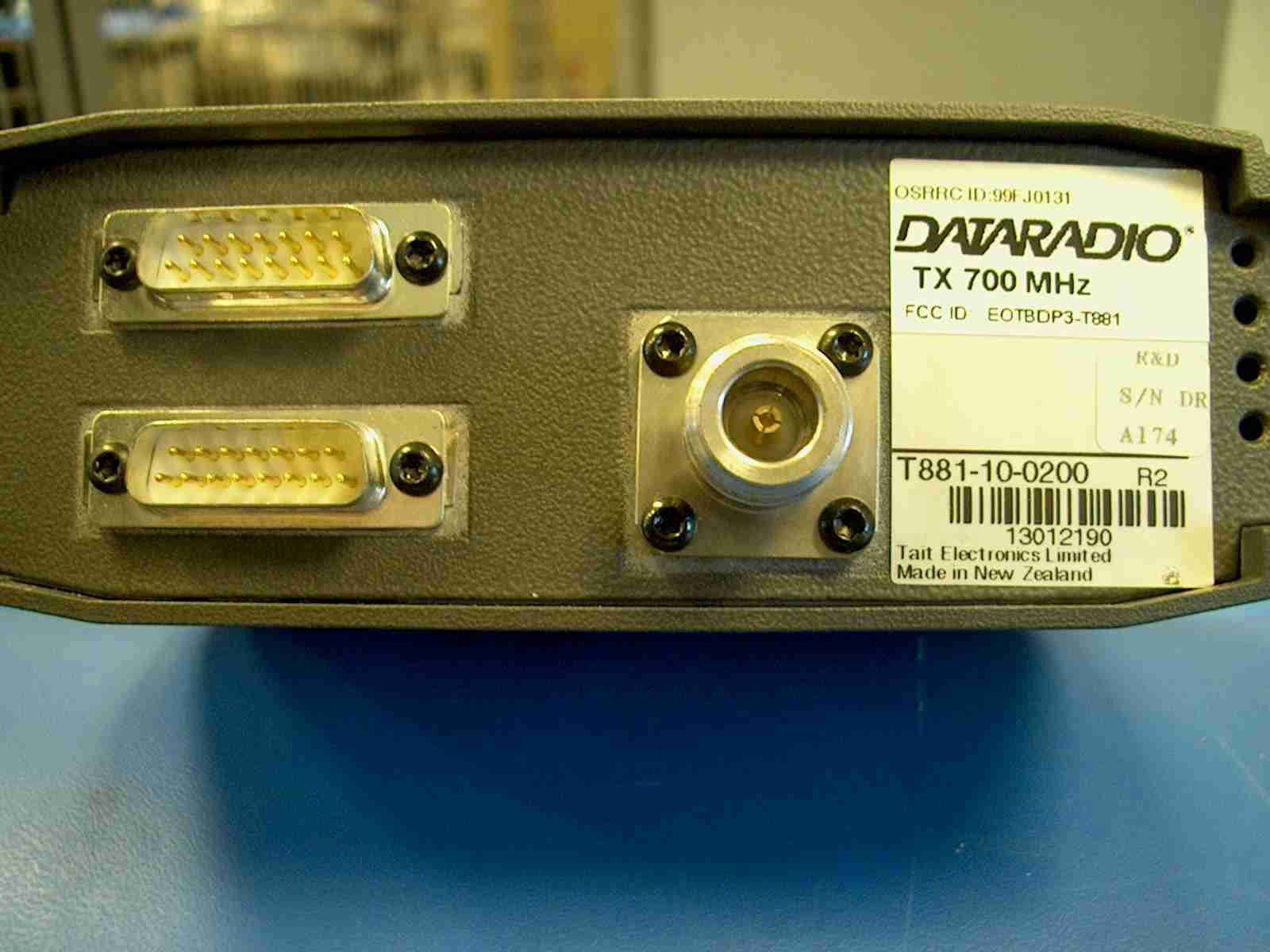
EOTBDP3-T881Paragon III
CALAMP WIRELESS NETWORKS INC.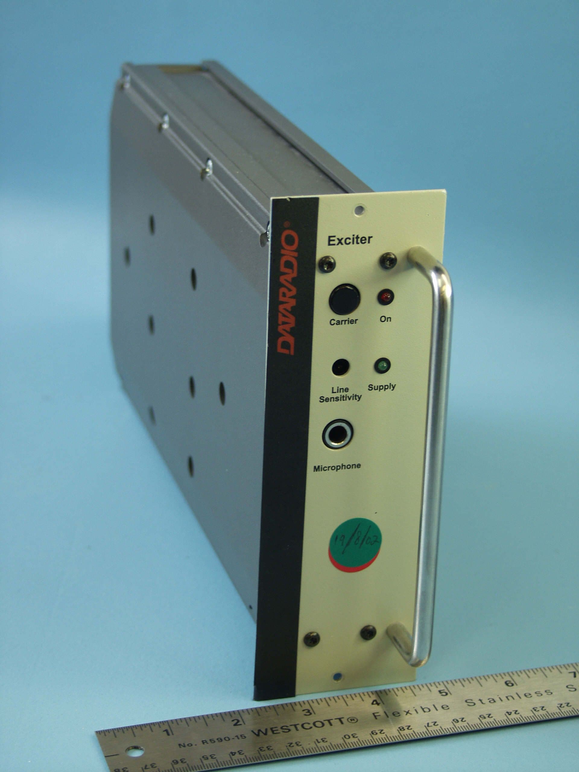
Click to zoom
Application Details
- Equipment Class
- TNB - Licensed Non-Broadcast Station Transmitter
- Date of Grant
- Aug 08, 2004
- Application Purpose
- Original Equipment
- Date of Application
- Jun 17, 2004
- Equipment Note
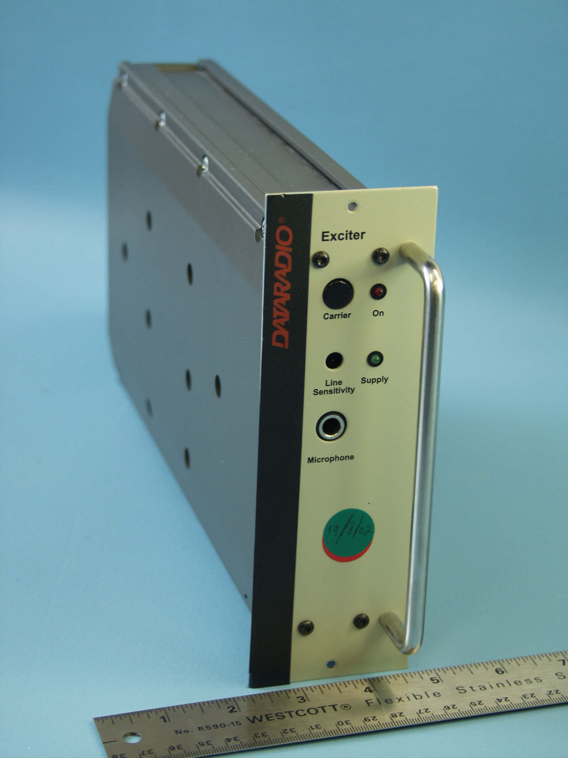
- Paragon III
- Frequency Range
- 762.00000000 - 773.00000000
- Country
- United States
Documents & Files
Document Text
Text extracted from the exhibit documents filed with the FCC. Open a document above to read the original.
Users Manual
Paragon-III (700 MHz) Data Base Station Technical Manual Version 0.01 (preliminary) The entire contents of this manual and the Radio Installation Software described in this manual are copyright 2004 by DATARADIO Inc. Copyright DATARADIO Inc. April 2004 Part no.: 120 20191-001 120 20191-001Paragon-III Technical Manual ii 1.PRODUCT OVERVIEW................................................................................................................................... 1 1.1 I NTENDED A UDIENCE ....................................................................................................................................... 1 1.2 G ENERAL D ESCRIPTION .................................................................................................................................... 1 1.2.1Features: ................................................................................................................................................. 2 1.3 F ACTORY T ECHNICAL S UPPORT ........................................................................................................................ 3 1.4 P RODUCT W ARRANTY ...................................................................................................................................... 4 1.5 R EPLACEMENT P ARTS ....................................................................................................................................... 4 1.5.1Factory Repair ........................................................................................................................................ 4 1.6 P ACKAGING ...................................................................................................................................................... 4 2.INSTALLATION ............................................................................................................................................... 5 2.1 O VERVIEW ........................................................................................................................................................ 5 2.2 L OCATION ......................................................................................................................................................... 5 2.3 F RONT V IEW :.................................................................................................................................................... 5 2.4 R EAR V IEWS : .................................................................................................................................................... 6 2.5 E LECTRICAL ...................................................................................................................................................... 8 2.5.1Paragon-III Assembly Power .................................................................................................................. 8 2.6 A NTENNA ....................................................................................................................................................... 10 2.6.1Overview ............................................................................................................................................... 10 2.6.2Cabling and Connection ....................................................................................................................... 10 2.7 C OMPLETING THE PHYSICAL I NSTALLATION .................................................................................................... 10 2.8 C HECKING OUT N ORMAL O PERATION ............................................................................................................. 10 3.OPERATING DESCRIPTION ....................................................................................................................... 11 3.1 R ADIO A SSEMBLY ........................................................................................................................................... 11 Receiver module ................................................................................................................................................. 11 3.1.25W Transmitter module ......................................................................................................................... 12 BDLC-III module ............................................................................................................................................... 12 3.1.4Speaker panel ........................................................................................................................................ 13 3.1.5Dual Power Supply module................................................................................................................... 13 3.1.6Radio Backplane Assembly ................................................................................................................... 14 4.TROUBLE-SHOOTING AND TESTING ..................................................................................................... 15 4.1 E QUIPMENT R EQUIRED ................................................................................................................................... 15 4.2 R ECOMMENDED C HECKS ................................................................................................................................15 4.3 A DDITIONAL TEST DETAILS ............................................................................................................................. 19 4.3.1RF Data Link Test ................................................................................................................................. 19 5.RADIO PROGRAMMING AND ADJUSTMENTS ..................................................................................... 20 5.1 S ERIES II R ADIO P ROGRAMMING .................................................................................................................... 20 5.1.1Rec…
Text truncated - open the document above for the full version.
Cover Letter(s)
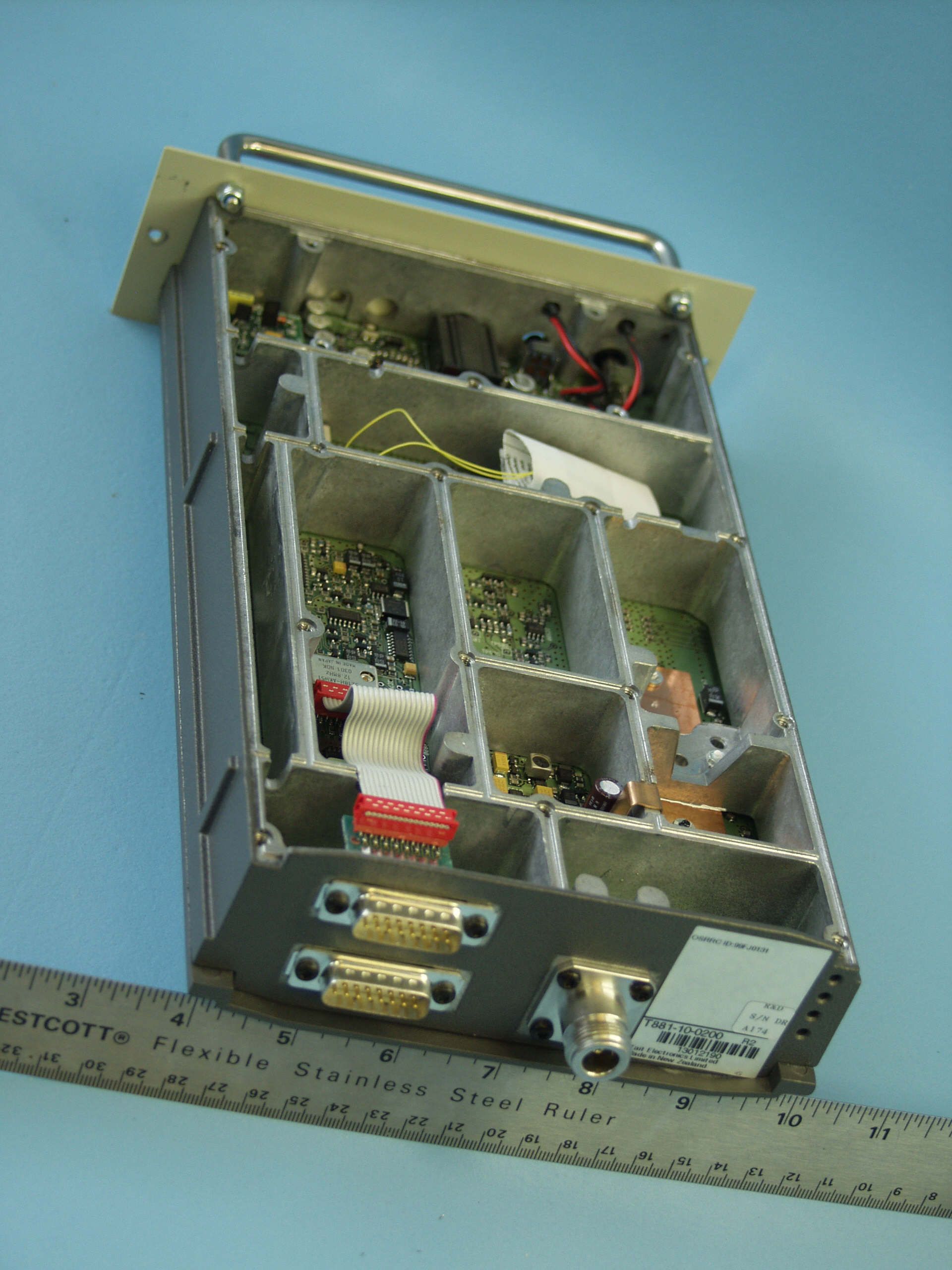
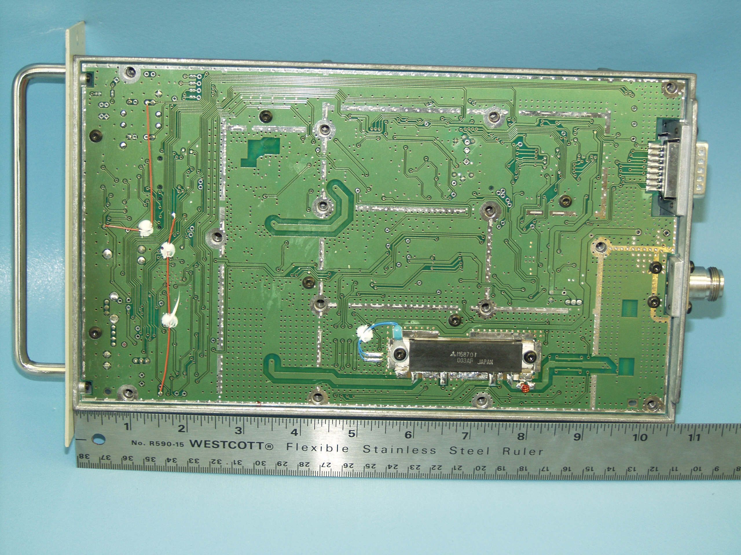
FCC ID EOTBDP3-T881 Applicant Dataradio Inc. Request for Confidentiality for: Annex A2- Digital Modulation Techniques. Annex B - Circuit Description Annexes E and E1 -Schematics Annexes F1 and F2 - Internal Pictures The request for confidentiality as per FCC 0.459 (a) refers to the above mentioned exhibits uploaded as Annexes of the report. These parts contains proprietary detail of the internal workings of the product and its protocol, the publication of which could be detrimental to our firm if taken out of context by competitors. For these reasons we request that the above mentioned documents be made confidential as per FCC 0.457(d)(2). Best Regards, Norman Pearl VP Engineering Dataradio Inc
Cover Letter(s)
FCC ID EOTBDP3-T881 Applicant Dataradio Inc. Request for Confidentiality ( Modified Jul 23, 2004) for: Annex A2- Digital Modulation Techniques. Annex B - Circuit Description Annexes E and E1 -Schematics The request for confidentiality as per FCC 0.459 (a) refers to the above mentioned exhibits uploaded as Annexes of the report. These parts contains proprietary detail of the internal workings of the product and its protocol, the publication of which could be detrimental to our firm if taken out of context by competitors. For these reasons we request that the above mentioned documents be made confidential as per FCC 0.457(d)(2). Best Regards, Norman Pearl VP Engineering Dataradio Inc
Parts List/Tune Up Info
BDP3-T881 –Dataradio Engineering Report – Annex C – Active part list E Page 1 of 2 156-90000-743 Dataradio© FCC submission ANNEX C TEST DATA Section Rule Part Number: 2.1033 (c)(10) Note: %D205 and %D210 are optional level limiting diodes for special applications. =R705 (47 ohm) and =SK710 are fitted in place of =IC700 when an external frequency reference is used. These two components are supplied with the auxiliary D-range kits (T800-06-0000 & T800-06-0001). Ref Var IPN Description CV300 028-11500-00 CAP TRIM 0.6/4.5 P SAPPHIRE %D111A 001-10015-50 DIODE SMD ZENER 1.5SMC22AT3 D211 008-00014-80 S) LED 3MM GREEN WITH WIRE D212 008-00014-79 S) LED 3MM RED WITH WIRE D220 001-10000-99 S) DIODE SMD BAV99 D-SW SOT23 D230 001-10010-40 DIODE SMD ZENER 33V BZG03-C33 D240 001-10000-56 S) DIODE SMD BAW56 D-SW SOT23 D250 001-10000-56 S) DIODE SMD BAW56 D-SW SOT23 D260 001-10000-56 S) DIODE SMD BAW56 D-SW SOT23 D270 001-10000-99 S) DIODE SMD BAV99 D-SW SOT23 D300 001-10005-35 S) DIODE SMD VCAP BB535 SOD323 D301 001-10005-35 S) DIODE SMD VCAP BB535 SOD323 D305 001-10005-35 S) DIODE SMD VCAP BB535 SOD323 D307 001-10005-35 S) DIODE SMD VCAP BB535 SOD323 D308 001-10063-05 DIODE SMD BAR63-05W SOT323 D400 001-10066-00 DIODE SCHOTTKY HSMS2815 D401 001-10066-00 DIODE SCHOTTKY HSMS2815 D610 001-10000-99 S) DIODE SMD BAV99 D-SW SOT23 D620 001-10000-70 S) DIODE SMD BAV70 D-SW SOT23 D630 001-10000-70 S) DIODE SMD BAV70 D-SW SOT23 D635A 001-10165-00 DIODE SCHOTTKY BAT165 SOD-323 D640 001-10000-70 S) DIODE SMD BAV70 D-SW SOT23 D645 001-10010-40 DIODE SMD ZENER 33V BZG03-C33 D710 001-10000-99 S) DIODE SMD BAV99 D-SW SOT23 D720 001-10000-99 S) DIODE SMD BAV99 D-SW SOT23 D730 001-10165-00 DIODE SCHOTTKY BAT165 SOD-323 D732 001-10165-00 DIODE SCHOTTKY BAT165 SOD-323 D810 001-10165-00 DIODE SCHOTTKY BAT165 SOD-323 IC210 002-10003-24 S) IC SMD 324 4X O-AMP SO14 IC220 002-10126-70 S) IC SMD DS1267S10K 2XDIG POT IC230 002-10003-24 S) IC SMD 324 4X O-AMP SO14 IC240 002-10040-53 S) MC14053B SMD BREAK B4 MAKE IC250 002-10020-50 IC SMD 4N25A OPTOCOUPLER IC260 002-10003-24 S) IC SMD 324 4X O-AMP SO14 #IC400 10 004-68701-00 MODULE M68701 806-870MHZ 6W #IC400 15 004-68701-00 MODULE M68701 806-870MHZ 6W #IC400 20 004-68701-01 MODULE M68701M 860-910MHZ 6W #IC400 25 004-68701-01 MODULE M68701M 860-910MHZ 6W #IC400 30 004-68701-02 MODULE M68701H 890-960MHZ 6W #IC400 35 004-68701-02 MODULE M68701H 890-960MHZ 6W IC500 002-10003-58 S) IC SMD LM358 DUAL O-AMP IC510 002-10006-60 S) IC SMD LMC660CM 4X O-AMP IC610 002-10078-05 S) IC SMD 78L05 5V REG IC630 002-12523-17(S) IC LM317L REG0.5A TO-252 IC640 002-10003-58 S) IC SMD LM358 DUAL O-AMP IC650 002-10012-32 SMD DS1232LP S-2 LP RESET&W-DOG =IC700 539-00010-55 TCXO 12.8M 1PPM- 20+70/2PPM-30 IC710 002-74904-00 IC SMD 74HC04A 6X INV BUFFD IC720 002-74910-04 S) IC SMD 74HCU04 6X INV IC730 002-10045-20 S) IC SMD 74HC4520T 2XCTR4BIT IC740 002-14519-10 S) IC SMD MC145191F SYNTH IC750 002-10330-78 S) IC MC33078D 2X AMP LO NOISE IC820 002-12416-00 S) IC SMD AT24C16N-10SC EEPROM IC830 002-10003-24 S) IC SMD 324 4X O-AMP SO14 PL201 240-00021-03 LIM) HEADER SMD 2X7WAY PL202 240-00021-03 LIM) HEADER SMD 2X7WAY Q210 000-10008-48 S) XSTR SMD BCW60 NPN SOT23 SS Q220 000-10008-17 S) XSTR SMD BC817-25 NPN SOT23 Q230 000-10008-48 S) XSTR SMD BCW60 NPN SOT23 SS Q240 000-10008-48 S) XSTR SMD BCW60 NPN SOT23 SS Q250 000-10008-17 S) XSTR SMD BC817-25 NPN SOT23 Q260 000-10008-57 S) XSTR SMD BCW70 PNP SOT23 SS Q270 000-10004-10 S) XSTR SMD MJD41C NPN SW DPAK Q300 000-10008-48 S) XSTR SMD BCW60 NPN SOT23 SS Q301 000-10008-48 S) XSTR SMD BCW60 NPN SOT23 Q302 000-10009-41 S) XSTR SMD BR941L SOT23 SS Q303 000-10009-41 S) XSTR SMD BR941L SOT23 Q304 000-10008-07 S) XSTR SMD BC807 PNP SOT23 AF Q305 000-10008-07 S) XSTR SMD BC807 PNP SOT23 AF Q307 000-10008-07 S) XSTR SMD BC807 PNP SOT23 AF Q308 002-10003-18 IC BGA318 MMIC AMPLIFIER BDP3-T881 –Dataradio Engineering Report – Annex C – Active part list E Page 2 of 2 156-90000-743 Dataradio© FCC submission Ref Var IPN Description Q309 000-10009-30 XSTR SMD BFR93A NPN SOT23 Q310 000-10008-07 S) XSTR SMD BC807 PNP SOT23 AF Q311 000-10008-07 S) XSTR SMD BC807 PNP SOT23 AF Q312 000-10008-07 S) XSTR SMD BC807 PNP SOT23 AF Q313 000-10008-07 S) XSTR SMD BC807 PNP SOT23 AF Q314 000-10008-07 S) XSTR SMD BC807 PNP SOT23 AF Q316 000-10008-48 S) XSTR SMD BCW60 NPN SOT23 SS Q317 000-10008-07 S) XSTR SMD BC807 PNP SOT23 AF Q318 000-10008-07 S) XSTR SMD BC807 PNP SOT23 AF Q319 000-10080-00 XSTR SMD BLT80 UHF PWR SOT223 Q321 000-10008-07 S) XSTR SMD BC807 PNP SOT23 AF Q322 000-10008-48 S) XSTR SMD BCW60 NPN SOT23 SS Q500 000-10008-48 S) XSTR SMD BCW60 NPN SOT23 SS Q501 000-10008-48 S) XSTR SMD BCW60 NPN SOT23 SS Q502 000-10008-07 S) XSTR SMD BC807 PNP SOT23 AF Q503 000-10008-07 S) XSTR SMD BC807 PNP SOT23 AF Q505 000-10008-07 S) XSTR SMD BC807 PNP SOT23 AF Q506 000-10008-07 S) XSTR SMD BC807 PNP SOT23 AF Q507 000-10008-07 S) XSTR SMD BC807 PNP SOT23 AF Q508 000-10008-07 S) XSTR SMD BC807 PNP SOT23 AF Q510 000-10008-07 S) XSTR SMD BC807 PNP SOT23 AF Q511 000-10008-07 S) XSTR SMD BC807 PNP SOT23 AF Q512 000-10008-07 S) XSTR SMD BC807 PNP SOT23 AF Q513 000-10008-07 S) XSTR SMD BC807 PNP SOT23 AF Q515 000-10008-07 S) XSTR SMD BC807 PNP SOT23 AF Q516 000-10008-48 S) XSTR SMD BCW60 NPN SOT23 SS Q517 000-10008-48 S) XSTR SMD BCW60 NPN SOT23 SS Q610 000-10008-07 S) XSTR SMD BC807 PNP SOT23 AF Q620 000-00033-12 XSTR BD242 PNP ISOLTD TO-220 Q630 000-10003-00 S) XSTR BSR30 PNP AF SOT-89 Q660 000-10008-17 S) XSTR SMD BC817-25 NPN SOT23 Q670 000-10008-57 S) XSTR SMD BCW70 PNP SOT23 SS Q710 000-10008-48 S) XSTR SMD BCW60 NPN SOT23 SS Q720 000-10008-57 S) XSTR SMD BCW70 PNP SOT23 SS Q730 000-10008-48 S) XSTR SMD BCW60 NPN SOT23 SS Q740 000-10008-57 S) XSTR SMD BCW70 PNP SOT23 SS Q750 000-10008-07 S) XSTR SMD BC807 PNP SOT23 AF Q760 000-10008-48 S) XSTR SMD BCW60 NPN SOT23 SS Q770 000-10008-57 S) XSTR SMD BCW70 PNP SOT23 SS Q775 000-10008-57 S) XSTR SMD BCW70 PNP SOT23 SS Q780 000-10008-48 S) XSTR SMD BCW6…
Text truncated - open the document above for the full version.
Parts List/Tune Up Info
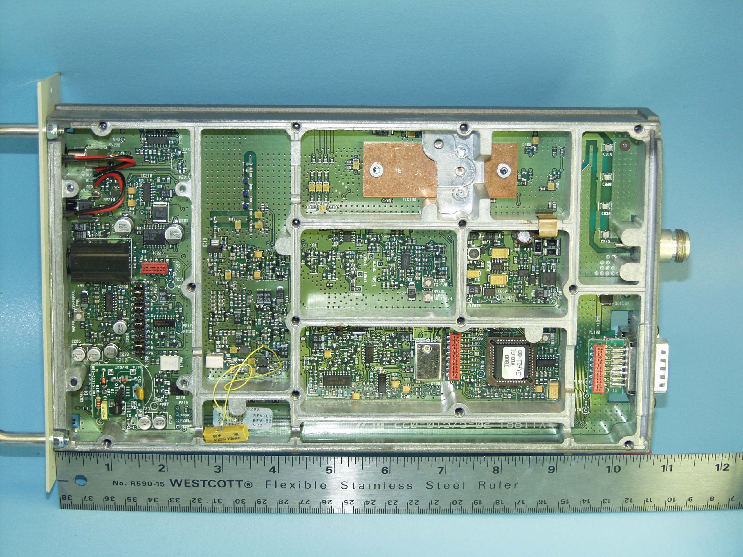
BDP3-T881 –Dataradio Engineering Report – Annex D page 1/3 156-90000-744 Dataradio© FCC submission Annex D TRANSMITTER TUNE UP PROCEDURE RULE PART NUMBER: 2.1033 c (9) Exciter Module (T881-xx-0200) (Excerpts from the technical manual pages 30-35) Note 1: Refer to Figure 1 (T881). Note 2: When the synthesizer is unlocked, the front panel green LED called "Supply" will flash indicating that it needs re-tuning. Warning: The LED will also flash when the unit is in setup mode while connected to the PGM800win program. Initial Setup 1. Shut down power to the base station. 2. Prepare the Multimeter to DC Volts. 3. Remove the exciter (T881) module from the base station rack frame. 4. Remove the exciter top cover (nearest the handle). 5. Connect a 3 feet long double shielded cable (N-M to BNC-M) between the IFR T/R output and the exciter antenna connector. 6. Connect the Paragon-III Extender Rail Kit to the empty chassis exciter slot. 7. Apply power to the base station. Synthesizer Alignment Single channel : Connect the Multimeter to either side of L309 (T881). - T881 (700 MHz) Tune VCO trimmer CV300 for a synthesizer loop voltage of 10V DC. Multiple channels (adjusting as shown for single channel above): - T881 (700 MHz) Adjust the VCO loop to 10V using the middle frequency channel. All channels should lie within the upper and lower limits of 16V and 3V respectively for the T881. Note: Normally, the fast TX key option is installed and the synthesizer is always energized. In the case where that option was not fitted, key the transmitter by pressing the front panel Carrier button to make the above adjustment possible. TX Frequency Error Adjustment 1. Apply the following settings to the IFR: - Receiver mode - IFR RX frequency to match the main radio TX frequency - IF Filter set to 30KHz - Zoom the RF Error window: select 10Khz range BDP3-T881 –Dataradio Engineering Report – Annex D page 2/3 156-90000-744 Dataradio© FCC submission 2. Key the transmitter by pressing the front panel TX-Key button and measure the carrier output frequency. It should be within ±300 Hz. If it is not, adjust the TCXO (IC700) to trim to meet the requirement, preferably within 100Hz. Low-Frequency Balance Adjustment Note: • PGM800Win version 3.00 or later must be used. Electronic potentiometer (256 step) is used to allow channel adjustment of two-point modulation (Low freq. balance). 1. Apply the following settings to the IFR: – Receiver mode and Oscilloscope display (Source Demod out connector, DC coupled). – IFR RX frequency to match the radio transmit frequency – IF Filter set to 30KHz – Zoom the Deviation window: select 10kHz Range and DC coupling. 2. Select the active or, the lowest (in the case of multi-channel base) frequency channel (via dip switch) 3. Transmit a square wave by using CDip (using a second serial port). 4. Press EPOTs button. Adjust IC220 via PGM800Win “reference modulation” to obtain the best square wave, no damping, no overshoot. (You can use either the mouse or up and down arrow keys). Record the deviation read. 5. For single-channel unit, proceed to step 8. 6. For multi-channel unit, select the highest frequency channel. Transmit a square wave from Dataradio’s test software. Record deviation again. 7. The difference in deviation between the two channels should be less than ±300Hz. If not, re-adjust IC220 to "average" the square wave shape on both channels until the spec is met. 8. To confirm the adjustment, select the active, or the lowest frequency channel. Compare the deviation produced between 1000 Hz sine wave test tone and Random data test pattern The difference between the test tone and the test pattern should be less than 1.9 kHz for (xRC16FSK ) For multi-channel unit, repeat this step on the highest frequency channel. 9. Select the active channel. Transmit a TX ON (Modulated) adjustment tone via CDip. Make sure that deviation levels read on the IFR correspond to 8kHz+5/-10%. Re-adjust deviation as necessary. Exciter Power Output 1. Apply the following settings to the IFR: - Receiver mode, Output T/R - IFR RX frequency to match the main radio TX frequency - IF Filter set to 30KHz - Select auto range in the Power reading window - Connect the coaxial cable from the IFR T/R to the Exciter output connector 2. Key the Exciter by pressing the module PTT button. The output power at the coaxial cable end connecting to the power amplifier should be: - T881 = 5W +0/-300mW (RV502, Figure 1) or the required output power in the range 1W-5W BDP3-T881 –Dataradio Engineering Report – Annex D page 3/3 156-90000-744 Dataradio© FCC submission Figure 1 - T881-0200 Exciter Tuning Controls locationignal before it reaches the T881 exciter.
Test Report
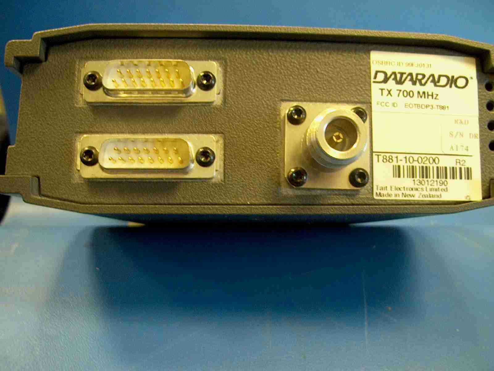
Engineering Exhibit in Support of Certification FCC Form 731 for the Digital Base Station Transmitter in 700MHz band FCC ID: EOTBDP3-T881 Trade Name: Dataradio P3 June 19 th , 2004 EOTBDP3-T881 – 700MHz Base Station Engineering Report - body Page 2 of 7 156-90000-740 Dataradio© FCC submission AFFIDAVIT The technical data included in this report has been accumulated through tests that were performed by me or by engineers under my direction. To the best of my knowledge, all of the data is true and correct. _______________________________________________________ Norman D Pearl Vice-president Engineering, Dataradio Inc. EOTBDP3-T881 – 700MHz Base Station Engineering Report - body Page 3 of 7 156-90000-740 Dataradio© FCC submission Dataradio Inc. Montreal, Canada ENGINEERING STATEMENT OF CONSTANTIN PINTILEI The application consisting of the attached engineering exhibit and associated FCC form 731 has been prepared in support of a request for Certification. Dataradio Inc requests certification for the 700 MHz 5W base station transmitter forming part of the data base station DATARADIO P3 . The modulation source of the base station is a model P3 - Basestation Data Link Controller (BDLC). The data base station will serve the fleet of mobile Gemini G3 approved under EOTGPD7, also manufactured by Dataradio Inc. The transmitter will operate in the frequency range 762-773 MHz, split into two bands of 762-764MHz and 767-773 MHz. Dataradio, Canada, purchases the OEM transmitter from Tait Electronics Inc, under part# T881-10 (see page 6 for part# description). Dataradio will modify it to fit digital transmission requirements of the P3 BDLC and perform final assembly of the Paragon P3 basestation. The transmitter along with the other components of the base station (receivers, BDLC, power supplies) will be identified by the Dataradio part number BDP3- 87S-RBWWWPM and marketed under the Model name P3. The transmitter based on T881 module will be identified by the FCC number EOTBDP3-T881. The transmitter operates pursuant to Part(s) 2,90 and 27 of the Rules and Regulations. The T881-10 Transmitter’s RF power is continuously variable from 1-5 watts and its nominal power is 5W. EXISTING CONDITIONS These Certification measurements were obtained using a production transmitter modulated by a prototype modem. The transceiver is designed to operate on frequencies ranging from 762.000 MHz to 773.000 MHz. The frequency tolerance of the transceiver is .0001% or 1.0 parts per million, controlled by a temperature compensated crystal oscillator (TCXO) operating at 12.8 MHz. PROPOSED CONDITIONS It is proposed to accept the request for the Dataradio P3 762-773 MHz 5W base station transmitter for operation in the band of frequencies previously outlined. The applicant anticipates marketing the device for use in wireless transmission of data. PERFORMANCE MEASUREMENTS All measurements were conducted in accordance with the code 47 CFR Section 2.1041and 2.1049 rev.2-167, Mar 15,2004, Section 90 Subpart R (90.521 to 90.555) rev 90-66 Sep 15, 2004 and Section 27 Subpart C rev Oct 1, 2001. Equipment performance measurements were made in the engineering laboratory of either Dataradio Inc, Montreal, Canada or subcontracted to Aprel Laboratories on the FCC certified Open Area Test Site at Nepean, Ontario, Canada. All measurements were made under my direction. The performance measurements were made between May 1 st , 2004 and June 3 rd , 2004 CONCLUSION Given the results of the measurements contained herein, the applicant requests that Certification be granted for the Dataradio P3, 762-773 MHz 5W digital base station transmitter as tested for data communications. 06/08/2004 Constantin Pintilei, Eng R&D Test Engineer, Dataradio Inc. EOTBDP3-T881 – 700MHz Base Station Engineering Report - body Page 4 of 7 156-90000-740 Dataradio© FCC submission TABLE OF CONTENTS AFFIDAVIT .............................................................................................................................................................................................. 2 ENGINEERING STATEMENT................................................................................................................................................................ 3 TABLE OF CONTENTS........................................................................................................................................................................... 4 QUALIFICATIONS OF ENGINEERING PERSONNEL ........................................................................................................................ 5 GENERAL INFORMATION ABOUT THE GRANTEE AND CERTIFICATED EQUIPMENT -2.1043 (b)(2) .................................. 6 OTHER DATA- Rule Part Number: 2.1033 (c).(3),(8),(9),(10),(11),(12),(13),(15),(16) ........................................................................ 7 ANNEXES( -document index): Annex A (-741): Test reports section. General.(2.1033c(14), 90.535(a)(c)90.543(e),27.54(e)) A1- Transmitter Rated Power Output (2.1046, 90.541) A2- Modulation characteristics (2.1047, 90.535) A3-Occupied bandwidth (2.1049, 90.543(d), 27.53(d)(4)) A4 -Spurious Emissons at Antenna Terminals (2.1051,90.543(c), 27.53(d) ) A5- Field Strength of Spurious Radiation (2.1053,90.543(c),27.53 (d)). Issued by Aprel Laboratories. A6- Frequency Stability vs Variation in Ambient Temperature (2.1055(a), 90.539,27.54) A7- Frequency Stability vs Variation in Supply Voltage (2.1055(d),90.539,27.54) A8- Emission Limitations (ACCP) (90.543 (a),(b)), 27.53(d) Annex B (-742): Circuit Description Annex C (-743): Transistor, Diode and IC Functions Annex D (-744): Transmitter Tune Up Procedure Annex E (-745): Schematics E1 – 5W Transmitter OEM schematics E2 – Schematic of the changes applied to OEM to fit digital modulation source Annex F (-746): Pictures: Label, External Photographs, Internal Photographs F1- Label F2- Internal Pictures F3- External pictures Annex G (-747): Instruc…
Text truncated - open the document above for the full version.
Test Report
BDP3-T881 –Dataradio Engineering Report – Annex A – Part A0 General (reference section) A0 Page 1 of 2 156-90000-741 Dataradio© FCC submission ANNEX A TEST DATA Section Rule Part Number: 2.1033 (c)(14) All applicable test data according to: -Part 2: 2.1046, 2.1047, 2.1049, 2.1051, 2.1053 and 2.1057 -Part 15:15.209 (15.207 does not apply) -Part 90, Subpart R: 90.521 to 90.555 -Part 27, Subpart C: 27.50 to 27.54 are provided in this section of the Engineering Report, as shown detailed below: part- pages Data Contents FCC parts Laboratory A0-2 General. Data efficiency Spurious radiation in the band 1559-1910MHz 2.1033 (c)(14) 90.535(a)(c) 90.543(e),27.53(e) A1-1 Transmitter Rated Power Output 2.1046, 90.541, 27.50(a)(2) R&D Dataradio Inc A2-1 Modulation characteristics 2.1047, 90.535 R&D Dataradio Inc A3-3 Occupied bandwidth 2.1049, 90.543(d),27.53(d)(4) R&D Dataradio Inc A4-2 Spurious Emissons at Antenna Terminals 2.1051,90.543(c),27.53(d)(3) R&D Dataradio Inc A5-19 Field Strength of Spurious Radiation 2.1053,90.543(c),(e),27.53(e) Aprel Laboratories A6-2 Frequency Stability vs Variation in Ambient Temperature 2.1055(a), 90.539,27.54 R&D Dataradio Inc A7-1 Frequency Stability vs Variation in Supply Voltage 2.1055(d),90.539,27.54 R&D Dataradio Inc A8- 14 Adjacent Channel Coupled Power 90.543(a),(b),27.53(d) R&D Dataradio Inc 44 Total number of report pages The following reports have been generated for FCC Certification of the Dataradio 742-776 MHz 5W Transmitter, part number BDP3- 87S-RBWWWPM. Unless otherwise noted, all of the measurements were conducted following the procedures set forth in the TIA/EIA-603 rev B standards. Set-up and equipment identification OEM transmitter unit (EUT): T881-10-0020 s/n: 13012187 Dataradio modulation source: prototype P3 , banner ID 200+DATARADIO Paragon-III G3[02] v1.00(Build:1) (CodeBase:SWINT_040520) +(Steve 200 P:1), DSP built DSP_1737Beta_RC4 Open Area Test Site (OATS): FCC certified Open Area Test Site at the Aprel Laboratories located at 51 Spectrum Way Nepean Ontario, Canada Modulation and Spectrum Usage Efficiency (90.535 (a)(c)) The unit employs only digital modulation as per 90.535 (a). The unit is designed for a channel size of 50 kHz as per 90.531(c) with a spectrum efficiency of 128kbps/50kHz . This equates to 128*3kbps/50*3kHz=384kbps/150kHz as required by 90.535(c) BDP3-T881 –Dataradio Engineering Report – Annex A – Part A0 General (reference section) A0 Page 2 of 2 156-90000-741 Dataradio© FCC submission The part 90.531(d)(2) states that two or three contiguous wideband (50 kHz) channels may be used in combination as 100 kHz or 150 kHz channels. Rates of 256kbps/100kHz and 384kbps/150 kHz respectively can be achieved running 3 units appropriately programmed Emissions in the band 1559-1610MHz (90.543(e),27.54(e)) The unit does not present any spurious products above the noise floor of the instrument in the mentioned band while set for frequencies in bands 762-764MHz or 767-773MHz. The noise floor of the instrument (Agilent 8563EC) was found to be – 90dBW/MHz also equated to –120dBm/Hz, this is 30dB better than required specification.
Test Report
BDP3-T881 –Dataradio Engineering Report – Annex A – Part A1 Transmitted power A1 Page 1 of 1 156-90000-741 Dataradio© FCC submission NAME OF TEST: Transmitter Rated Power Output RULE PART NUMBER: 2.1046 (a), 90.541 UNIT UNDER TEST T881-10-0020 sn 13012187 TEST RESULTS: 5W adjustable down to 1W see data below TEST CONDITIONS: Standard Test Conditions, 25 C TEST EQUIPMENT: Digital Voltmeter, Fluke 77 series II multimeter DC Power Supply , Astron Model VS-20M True RMS clamp multimeter, EXTECH instrument model 380947 Analog Wattmeter Coaxial Dynamics Inc model 81050, probe 500W Load 50ohm , 50W PERFORMED BY: DATE: 05/18/04 Constantin Pintilei TEST SET-UP: TEST RESULTS: Frequency (ch 120) (MHz ) DC Voltage at Final (VDC) DC Current into Final (ADC) DC Power into Final (W) RF Power Output (W) 772.975 13.68 1.51 20.66 5 772.975 13.74 0.85 11.68 1 Power Supply Radio under test Wattmeter CDI Ant. Pwr Connecto r Clamp Ampmeter Digital Voltmeter 50ohm 50W load
Test Report
BDP3-T881 – Dataradio P3 Engineering Report – Annex A – Part A3 Occupied Bandwidth A3 Page 1 of 3 156-90000-741 Dataradio© FCC submission Transmitter Occupied Bandwidth and Emission Designator Determination RULE PART NUMBER: 2.201, 2.202,2.1049 (h), 90.543(c),27.53(d)(4) Necessary Bandwidth Measurement (90.202.(c)(4)) and Emission Designator This radiomodem uses digital modulation signals, passing through a pulse shaping DSP implemented low-pass filter to an FM transceiver. The equations for the filter are Nyquist-based being driven by the data symbol rates, they are detailed in modulation source description paragraph, in next page. The necessary bandwidth calculation for this type of modulation is not covered by paragraphs (1), (2) or (3) from 2.202(c), the result exceeding by far the real necessary bandwidth obtained through simulations or measurement. Therefore, the approach outlined in (2.202(c)(4)) is applicable in this case. The results of 99% Occupied Bandwidth measurement are: Bit rate Deviation on 1kHz tone Deviation on random data Occupied Bandwidth 128 kbps ± 8.2 kHz ± 9.8 kHz 29000Hz 96 kbps ± 8.2 kHz ± 9.9 kHz 28670Hz 64 kbps ± 8.2 kHz ± 10.2 kHz 30000Hz The value of the necessary bandwidth (and implicitly of the emission designator) doesn’t exceed the authorized bandwidth of 50kHz (90.543(d)). Occupied Bandwidth Measurement (90.202(c)(4),90.543(b) The Occupied Bandwidth measurement option of the instrument (8563EC spectrum analyzer from Agilent) calculates and provides the values used above for the emission designator. The percentage setting of the measurement has been set to 99% following the definition of the Occupied Bandwidth “the frequency bandwidth such that, below its lower and above its upper frequency limits, the mean powers radiated are each equal to 0.5…
Text truncated - open the document above for the full version.
Contact Information
Applicant
Russell Cook(Director of Engineer)
[email protected]612-642-2127
Technical Contact
Dataradio IncConstantin Pintilei
[email protected]+1-514-737-0020
5500 Royalmount Ave, suite 200 · Town of Mont Royal · Canada
Technical Specifications
| # | Rule Parts | Frequency Range | Power Output | Emission | Tolerance |
|---|---|---|---|---|---|
| 1 | 27,90 | 762 MHz - 773 MHz | 5 W | 30K0F1D | 1.0000000000 ppm |
Other Applications from CALAMP WIRELESS NETWORKS INC.
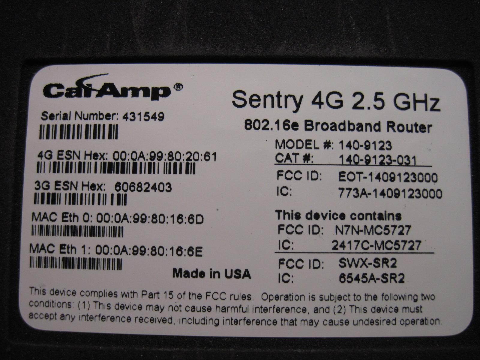
EOT-1409123000
May 15, 20112.5 GHz Wireless Broadband Route
Equipment Class
TNB - Licensed Non-Broadcast Station Transmitter
EOTBDP4-EXCT769
Sep 29, 2010700MHz Band SDR Exciter for BDP4 digital base station
Equipment Class
TNB - Licensed Non-Broadcast Station Transmitter
EOTBDP4-EXCT438
Jun 03, 2010UHF HIGH SDR Exciter for BDP4 digital base station
Equipment Class
TNB - Licensed Non-Broadcast Station Transmitter
EOTBDP4-EXCT403
Jun 02, 2010UHF LOW SDR Exciter for BDP4 digital base station
Equipment Class
TNB - Licensed Non-Broadcast Station Transmitter
EOT-1409290100
May 09, 2010900 MHz Broadband Base Station
Equipment Class
DTS - Digital Transmission System