EOTGPDAGemini/PD
CALAMP WIRELESS NETWORKS INC.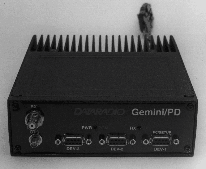
Click to zoom
Application Details
- Equipment Class
- TNB - Licensed Non-Broadcast Station Transmitter
- Date of Grant
- Mar 08, 1999
- Application Purpose
- Original Equipment
- Date of Application
- Dec 22, 1998
- Equipment Note
- Gemini/PD
- Frequency Range
- 403.00000000 - 512.00000000
- Country
- United States
Documents & Files
Document Text
Text extracted from the exhibit documents filed with the FCC. Open a document above to read the original.
Users Manual
Gemini / PD Mobile Radio Modem Service Manual version 0.03 PRELIMINARY The entire contents of this manual and the Radio Service Software described in this manual are copyright 1998 by DATARADIO Inc. Copyright DATARADIO Inc. November 1998 part no.: 120 1020110-003 i Table of Contents 1.PRODUCT OVERVIEW................................................................................................................................... 1 1.1 I NTENDED A UDIENCE ....................................................................................................................................... 1 1.2 G ENERAL D ESCRIPTION .................................................................................................................................... 1 1.3 C ONFIGURATION ............................................................................................................................................... 1 1.4 F ACTORY T ECHNICAL S UPPORT ........................................................................................................................ 2 1.5 P RODUCT W ARRANTY ...................................................................................................................................... 2 1.6 R EPLACEMENT P ARTS ....................................................................................................................................... 2 1.6.1Factory Repair ........................................................................................................................................ 2 2.OPERATION...................................................................................................................................................... 2 2.1 F RONT & R EAR P ANELS ................................................................................................................................... 2 2.1.1LED Indicators........................................................................................................................................ 3 2.2 DTE P ORT I NTERFACE ..................................................................................................................................... 3 2.2.1RS-232 Interface Signal Levels ............................................................................................................... 3 3.ADJUSTMENTS AND MAINTENANCE ....................................................................................................... 4 3.1 O VERVIEW ........................................................................................................................................................ 4 3.1 I NTENDED A UDIENCE ....................................................................................................................................... 4 3.2 E QUIPMENT R EQUIRED ..................................................................................................................................... 4 3.3 M AINTENANCE I NTERVALS ...............................................................................................................................4 3.4 T ESTS & A DJUSTMENTS ................................................................................................................................... 4 3.4.1Preliminary Verification ......................................................................................................................... 4 3.4.2Basic Tests & adjustments....................................................................................................................... 4 3.4.3Tests & adjustments Procedure............................................................................................................... 4 3.4.4Opening the Unit ..................................................................................................................................... 6 3.4.5GPS Diagnostics Procedure.................................................................................................................... 7 4.SPECIFICATIONS ............................................................................................................................................ 8 ii What's New in Version 0.02 GPS Diagnostics procedure History Version 0.1: First preliminary version Version 0.2: • Unit specification revised • Typo correction iii Definitions The following terms are used throughout this document. ItemDefinition DCEData Communications Equipment. This designation defines the direction (input or output) of the various RS-232C interface signals. Modems are always wired as DCE. See also DTE. DTEData Terminal Equipment. This designation defines the direction (input or out- put) of the various RS-232C interface signals. Most user equipment, as well as PCs, are wired as DTE. See also DCE. GCUGemini Control Unit board Gemini/PDHigh specs mobile radio modem. PD = Parallel decode HDXHalf Duplex. A unit which uses separate transmit and receive frequencies, but which may not transmit and receive simultaneously. RS-232Industry–standard interface for low speed data transfer (EIA-RS-232E). RSSRadio Service Software. This software allows configuration and testing of the Gemini/PD. SimplexA unit which uses the same frequency for transmit and receive. 120 20110-003 PRELIMINARYGemini/PD Technical Manual 1 1. PRODUCT OVERVIEW This document provides the information required for the operation and maintenance of the DATARADIO Gemini/PD mobile radio- modem. 1.1 Intended Audience This document is designed for use by engi- neering design, installation, and mainte- nance personnel. 1.2 General Description Gemini/PD is a mobile radio-modem aimed at the public safety and public utility markets to meet demand for high speed and high throughput. It integrates all the necessary hardware for data-only vehicular installations up to but not including the laptop PC and its application software. Example of applications are: 1. Database inquiry syste…
Text truncated - open the document above for the full version.
External Photos
EXTERNAL PHOTOS Figure 1 Front side external photo EXTERNAL PHOTOS Figure 2. Rear side external photo EXTERNAL PHOTOS Figure 3. Left side external photo (the label side)
ID Label/Location Info
FCC LABEL: RULE PART NUMBER:2.1033 c (11) Location Info: Left side close to rear left corner.
Internal Photos
INTERNAL PHOTOS Figure 1 Internal top view INTERNAL PHOTOS Figure 2Internal bottom view INTERNAL PHOTOS Figure 3Internal top view, service position. INTERNAL PHOTOS Figure 4 Internal top view, hidden side INTERNAL PHOTOS Figure 5 Internal, bottom view, hidden side INTERNAL PHOTOS Figure 6 Internal bottom view, service position
Operational Description
DESCRIPTION OF CIRCUITRY AND BLOCK DIAGRAMS RULE PART NUMBER:2.1033 (c)(10) MOBILE DATA PRODUCT POWER AMPLIFIER (PA) CIRCUIT BOARD CONNECTIONS Power and ignition sense are supplied to the radio through J650. Since the power is connected directly to the vehicle battery, the ignition sense line tells the radio when the vehicle ignition is on. The PA board connects to the RF board via J600, a 10-pin socket. This connector supplies power to the RF board through F600 and provides control over the PA board. CR600, a transorb prevents negative voltages and extremely high positive voltages from damaging the radio by conducting and blowing the 12A in-line fuse. The main antenna is connected to the PA board through J630, a mini-UHF connector. The transmitter output and main receiver input are provided through this 50 Ω connector. The main receiver signal is passed to the RF board through P200, a 50 Ω through-chassis connector. The transmit drive input comes from the RF board through P500, another 50 Ω through-chassis connector. PA TEMPERATURE SENSE One control signal provided to the RF board microprocessor is temperature sense. A thermistor (RT680 for 10W models, or RT690 for 40W models) is placed next to the final amplifier on the PA board and its resistance changes with the final amplifier temperature. The thermistor is biased by R405 on the RF board providing a voltage that varies linearly with temperature from 15°C to 125°C, the normal temperature range of the PA during use. If the final amplifier temperature exceeds a preset threshold, the microprocessor will fold back the power to prevent thermal destruction of the final. PA CURRENT SENSE Current to the final amplifier passes through R618 creating a proportional voltage across the resistor. U600B, CR614, CR616, R614, R615, R616, and R617 form a differential amplifier that amplifies the voltage across R618 and provide this voltage to the RF board microprocessor. When the final amplifier current exceeds a preset threshold due to high VSWR, the microprocessor will fold back the power to prevent thermal destruction of the final. PA FORWARD POWER SENSE The final amplifier output passes through a directional coupler that samples some of the transmit power and rectifies it through CR620 with C674 providing filtering of the RF content. Resistors R636 and R637 drop the voltage down to a suitable level for the microprocessor. The power sense voltage is proportional to the square root of the output power. PRE-TRANSMIT ENABLE The pre-transmit enable signal from the RF board prepares the PA board for transmit. The pre-driver, Q670, and driver, Q680, are biased on, and the antenna switch is configured for transmit by turning on CR640 and CR650. TRANSMIT ENABLE The transmit enable signal pulls the power control amplifier U600A out of saturation and allows the PA power to reach the programmed output level. When transmit enable is removed, U600A goes into saturation again causing the output power to drop to zero. POWER CONTROL AND DRIVE BUFFER The power set voltage from the RF board is applied to the non-inverting input of U600A. The PA forward power sense voltage is fed into the inverting input of U600A through CR605, R601 and R603. The output of U600A is fed into a high current amplifier consisting of Q640, Q650, R606, R607, and R608. This amplifier has a voltage gain of approximately two. The output of the high current amplifier provides bias and collector current for Q665, the drive buffer. When the power set voltage is greater than the forward power voltage, U660A turns the high current amplifier on harder increasing the bias to Q665, and providing more drive level. When the forward power voltage is greater than the power set voltage, U660A cuts the high current amplifier level down decreasing the bias to Q665, and reducing drive level. The input to Q665 is from the PA buffer on the RF board through an attenuator formed by R619, R620, and R621. C623 and C624 provide the input match, with feedback from C625 and R624 for stability. The output of Q665 goes to the pre-driver Q670 with C626, C629, and C630 providing the interstage match. 3-WATT PRE-DRIVER Transistor Q670 is a 3-Watt vertical MOSFET that provides pre-drive level for the 40W model and drive level for the 10W model. The output of this stage goes to Q680 with C639, C640, C641, C642, L602, and C643 providing the interstage match. 15-WATT DRIVER / FINAL (10W Model) Transistor Q680 is a 15-Watt vertical MOSFET that provides drive level for the 40W model and is the final amplifier for the 10W model. The output of this stage goes to Q680 in the 40W model or is matched to 50 Ω=in the 10W model. The interstage match consists of C651, C652, C653, L604, C656, C657, and C658. The 10W final match consists of C651, C652, C653, L604, C656, MP690, L608, C666, and C667. 50-WATT FINAL (40W Model Only) Transistor Q690 is a 50-Watt bipolar transistor that is the final amplifier for the 40W model. The output of this stage is matched to 50 Ω using C664, C665, C666, L608, C667, and C668. ANTENNA SWITCH In receive, CR640 and CR650 are biased off and the main receive signal passes from J630, through the low pass filter, forward power detector, L610, C672, and C671 to P200, the RF board main receive input. In transmit, CR640 and CR650 are biased on, shorting the transmit path to the forward power detector and the receive path to ground. When the receive path is grounded, a high impedance is provided from a discrete quarter-wave section formed by C669, L610, and C670 to the transmit path providing rejection between the transmitter and the receiver. LOW PASS FILTER To reduce the harmonic content of the final amplifier, the transmit signal passes through a 7-pole low pass filter to the antenna. The low pass filter consists of C678, L612, C679, L614, C680, L616, and C681. R640 bleeds static charge from the antenna to protect the active devices in the power amplifier. RADIO FREQUENCY (RF) CIRCUIT BOARD CONNECTIONS The RF bo…
Text truncated - open the document above for the full version.
Parts List/Tune Up Info
TRANSISTOR, DIODE, AND IC FUNCTIONS RULE PART NUMBER:2.1033 c (10) MDP TRANSCEIVER Manufacturer Part# JDT Part#ReferencesFunction BB535623-5005-022CR139Diode for Cap Multiplier MMBV609623-5005-023CR1402nd LO Tuning Varactor MMBV3401623-1504-001CR202Transmit to Receive Switch BB535623-5005-022CR210RX Front End 2 Pole Preselector Main RX BB535623-5005-022CR211RX Front End 2 Pole Preselector Main RX MMBD6050623-1504-002CR220LNA Overload Protection Diode Main RX BB535623-5005-022CR230RX Front End 3 Pole Preselector Main RX BB535623-5005-022CR231RX Front End 3 Pole Preselector Main RX BB535623-5005-022CR232RX Front End 3 Pole Preselector Main RX BB535623-5005-022CR233RX Front End 3 Pole Preselector Main RX BB535623-5005-022CR236RX Front End 3 Pole Preselector Main RX BB535623-5005-022CR237RX Front End 3 Pole Preselector Main RX BZX84C623-2016-519CR30Flash Voltage Switch BB535623-5005-022CR310RX Front End 2 Pole Preselector Diversity RX BB535623-5005-022CR311RX Front End 2 Pole Preselector Diversity RX MMBD6050623-1504-002CR320LNA Overload Protection Diode Diversity RX BB535623-5005-022CR330RX Front End 3 Pole Preselector Diversity RX BB535623-5005-022CR331RX Front End 3 Pole Preselector Diversity RX BB535623-5005-022CR332RX Front End 3 Pole Preselector Diversity RX BB535623-5005-022CR333RX Front End 3 Pole Preselector Diversity RX BB535623-5005-022CR336RX Front End 3 Pole Preselector Diversity RX BB535623-5005-022CR337RX Front End 3 Pole Preselector Diversity RX BZX84C623-2016-519CR453Protection Diode BZX84C623-2016-519CR456Protection Diode BZX84C623-2016-519CR457Protection Diode BZX84C623-2016-519CR485Protection Diode BZX84C623-2016-519CR486Protection Diode BZX84C623-2016-519CR488Protection Diode MR2535L623-2906-001CR600Voltage Suppressor BB535623-5005-022CR605Power Control Diode BB535623-5005-022CR610TX Enable Diode BB535623-5005-022CR614Drop V Below Op-Amp Rail V for Current Sense BB535623-5005-022CR616Drop V Below Op-Amp Rail V for Current Sense MMBD701LT1623-1504-016CR620Antenna Switch BZX84C623-2016-519CR630Power Control Limit MA47059623-1504-032CR640Antenna Switch MA47059623-1504-032CR650Antenna Switch MBAV99623-1504-023CR70Negative Voltage Regulator MBAV99623-1504-023CR72Negative Voltage Regulator BZX84C623-2016-519CR78Protection Diode BB535623-5005-022CR805Diode for Cap Multiplier BB535623-5005-022CR900Modulation Varactor BB535623-5005-022CR904VCO Varactor, Freq Tuning BB535623-5005-022CR906VCO Varactor, Freq Tuning TRANSISTOR, DIODE, AND IC FUNCTIONS (Continued) RULE PART NUMBER:2.1033 c (10) Manufacturer Part# JDT Part#ReferencesFunction BB535623-5005-022CR908VCO Varactor, Freq Tuning BB535623-5005-022CR910VCO Varactor, Freq Tuning 4035623-1504-035CR912VCO TX Pin Shift MUN5213T1676-0013-046Q10RF Enable Override MSD1819A676-0013-701Q11Modem RF Enable MSB1218A676-0013-700Q110RX 1st LO Buffer Amplifier Active Bias MRF9411676-0003-618Q111RX 1st LO Buffer Amplifier MSD1819A676-0013-701Q12Auxiliary RF Enable MSD1819A676-0013-701Q13Auxiliary RF Enable MSD1819A676-0013-701Q139Cap Multiplier on 2nd LO VCO Buffer MMBT918676-0003-634Q140RX 2nd LO Oscillator MMBT918676-0003-634Q1412nd LO Buffer Amplifier MUN5114T1676-0013-032Q20Transceiver Enable MUN5213T1676-0013-046Q21Transceiver Enable MSB1218A676-0013-700Q220RX LNA Active Bias Main RX MRF9411676-0003-618Q221RX LNA Main RX MMBT918676-0003-634Q250IF Amplifier Main RX MSB1218A676-0013-700Q2601st LO Amplifier Main RX MRF9411676-0003-618Q2611st LO Amplifier Main RX MMBT918676-0003-634Q2702nd LO Supply Switch MUN5114T1676-0013-032Q30Flash Voltage Switch MSD1819A676-0013-701Q31Flash Voltage Switch MSB1218A676-0013-700Q320Diversity LNA Bias MRF9411676-0003-618Q321Diversity LNA MMBT918676-0003-634Q350IF Amplifier Diversity RX MSB1218A676-0013-700Q3601st LO Amplifier Diversity RX MRF9411676-0003-618Q3611st LO Amplifier Diversity RX MMBT918676-0003-634Q3702nd LO Supply Switch MJD42C676-0002-603Q409.6 V Regulator MMBT3904676-0003-658Q419.6 V Regulator MUN5213T1676-0013-046Q410SCI Control Switch MMBT4403676-0003-612Q505.5 V Regulator MMBT4403676-0003-612Q515.5 V Regulator MSB1218A676-0013-700Q510Transmitter Driver Active Bias MMBT3904676-0003-658Q525.5 V Regulator MRF9411676-0003-618Q520Transmitter Driver MSA2111676-0003-640Q550Buffer/Amp for Transmitter Driver MUN5213T1676-0013-046Q600TX_Enable MMBT3904676-0003-658Q6209.6PTx Antenna Switch MMBT3904676-0003-658Q630Power Control MJD42C676-0002-603Q640Power Control MMBT3904676-0003-658Q650Power Control MMBT3904676-0003-658Q660Power Control MRF5812676-0003-604Q665Transmitter 250 mW MRF5003676-0006-450Q6703 W Predriver MRF5015676-0006-150Q68015W Driver TRANSISTOR, DIODE, AND IC FUNCTIONS (Continued) RULE PART NUMBER:2.1033 c (10) Manufacturer Part# JDT Part#ReferencesFunction MRF650676-0004-402Q69050 W Final MSB1218A676-0013-700Q70Negative Voltage Regulator MSB1218A676-0013-700Q71Negative Voltage Regulator MSB1218A676-0013-700Q72Negative Voltage Regulator MSD1819A676-0013-701Q73Negative Voltage Regulator MSD1819A676-0013-701Q74Negative Voltage Regulator MSD1819A676-0013-701Q805Cap Multiplier on VCO MUN5114T1676-0013-032Q820VCO Pin Shift MUN5213T1676-0013-046Q821VCO Pin Shift MMBT4403676-0003-612Q90Main RX enable NE85633676-0003-636Q900VCO NE85633676-0003-636Q902VCO Amplifier NE85633676-0003-636Q904VCO Cascode Amplifier NE85633676-0003-636Q906VCO Buffer Amplifier MUN5213T1676-0013-046Q91Main RX enable MMBT4403676-0003-612Q92Diversity RX enable MUN5213T1676-0013-046Q93Diversity RX enable MMBT4403676-0003-612Q94TX Pre-Transmit Enable MUN5213T1676-0013-046Q95TX Pre-Transmit Enable LP2951644-2003-067U105.0 V Regulator MC14053B644-3016-053U110Mod IN Narrow/Wide Band Switch MC33172D644-2019-017U120Audio Out Amp Main RX MC33464644-MC33464-U20MicroController Reset MC33172D644-2019-017U208Audio Out Amp Diversity RX LRMS-2MH644-0007-018U250First Mixer Main RX SA676DK644-2002-037U260IF IC Main RX LRMS-2MH644-0007-018U350First Mixer Diversity RX SA676DK644-2002-037U360IF IC Diversity RX MC33172D644-2019-017U405.5, 9.6 …
Text truncated - open the document above for the full version.
Schematics
Dataradio© EOTGPDA FCC report-Appendix Schematics Gemini/PD schematics Contents MDP Transceiver...................................pag 2-4Gemini Modem/loader ............................pag 5-8 EOTGPDA FCC report-Appendix Schematics- Gemini/PD schematics 2/8 Dataradio© JIC R12MC33164D U20 4 GND 2 INPUT 1 _RESET 8 NC8 7 NC7 6 NC6 5 NC5 3 NC3 U410 74HC125 6 2Y 11 4Y 10 _3OE 8 3Y 14 VCC 12 4A 4 _2OE 2 1A 7 GND 9 3A 1 _1OE 13 _4OE 5 2A 3 1Y Q13MSD1819A 0.01 C417 22K R407 R408 22K 0.01 C415 C10 1 4.7 C44 1 C414 1 C93 1 C92 1 C91 1 C54 1 C11 MC68HC908AZ60 U420 46 PTD2 47 PTD3 8 PTF4|TBCH0 7 PTF3 16 PTE3|TACH1 57 CGMXFC 9 CANRX 10 CANTX 12 PTF6 4 PTF0|TACH2 20 PTE7|SPSCK 6 PTF2 48 PTH0|KBD3 33 PTA7 18 PTE5|MISO 44 VDDAREF 55 VDDA 61 PTC1 15 PTE2|TACH0 14 PTE1|RXD 13 PTE0|TXD 25 PTG2|KBD2 24 PTG1|KBD1 11 PTF5|TBCH1 21 VSS 56 VSSA 41 PTB7|ATD7 5 PTF1|TACH3 54 VREFH 19 PTE6|MOSI 60 PTC0 31 PTA5 3 _RST 2 _IRQ 23 PTG0|KBD0 52 PTD6|TACLK 17 PTE4|_SS 29 PTA3 30 PTA4 32 PTA6 34 PTB0|ATD0 35 PTB1|ATD1 36 PTB2|ATD2 37 PTB3|ATD3 38 PTB4|ATD4 26 PTA0 27 PTA1 28 PTA2 62 PTC2|MCLK 63 PTC3 1 PTC4 64 PTC5 39 PTB5|ATD5 40 PTB6|ATD6 45 AVSS|VREFL 50 PTD4|TBCLK 51 PTD5 58 OSC2 49 PTH1|KBD4 53 PTD7 42 PTD0 43 PTD1 59 OSC1 22 VDD MSD1819AQ12 100KR415 1.15K 1% R405 10K R406 C444 0.010.01 C439C434 0.010.01 C429 4.7 C72 4.7 C71 4.7 C70 4.7 C73 0.01C74 100pF C470 1.0uH L401 100pF C90 100pF C22 100pF C488 100pF C487 100pF C486 100pF C485 100pF C484 100pF C483 100pF C480 100pF C479 100pF C478 100pF C477 100pF C476 100pF C475 100pF C474 100pF C473 100pF C472 100pF C471 100pF C469 100pF C468 100pF C467 100pF C466 100pF C465 100pF C460 100pF C459 100pF C458 100pF C457 100pF C456 100pF C455 100pF C454 100pF C453 100pF C452 100pF C451 100pF C450 100pF C406 100pF C405 100pF C404 100pF C403 100pF C402 100pF C407 100pF C408 100pF C409 100pF C410 100pF C45 0.01C43 100pF C55 0.01 C53 100pF C50 0.01 C30 0.01 C13 0.01 C14 0.001 C17 0.001C443 0.001C442 0.01 C441 0.001C438 0.001 C437 0.01 C436 0.001 C433 0.001 C432 0.01 C431 0.01 C426 0.001C428 0.001C427 JIC C12 0.1 C413 0.1 C412 JIC C416 10KR13 0.01 C420 22pFC419 22pFC418 1K R463 100K R462 10K R422 10K R417 10K R416 10K R412 10K R410 10K R403 10K R404 JIC R453 JIC R443 JIC R433 JIC R423 APER JDT 4.7K R472 4.7K R471 4.7K R470 15K R456 15K R446 15K R436 15K R426 120K R458 120K R448 120K R438 120K R428 180K R455 180K R445 470 R467 470 R466 470 R465 470 R464 470 R460 470 R474 470 R476 470 R477 470 R478 470 R480 470 R482 470 R484 10K R486 10K R488 470 R489 470 R492 470 R493 470 R494 470 R495 10K R95 10K R93 10KR91 1K R71 JIC R70 10K R75 10K R76 10K R74 12K R55 10K R56 10KR53 10K R50 10KR41 10K R40 10K R30 100K R31 100KR421 10K R420 1MEGR418 100KR414 100KR413 30K R402 100K R411 100K R11 100K R94 100K R92 100K R90 100K R490 100K R487 100K R485 100K R483 100KR481100K R479 100K R475 100 R80 470 R32 470R42 180K R78 180K R435 180K R425 220KR424 220KR427 JIC R434 220KR437 220KR444 220KR447 JIC R454 220KR457 51K R35 51K R461 51K R473 51KR1851KR16 51K R17 51KR15 12K R491 100R51 100 R52 F401 2A 15K R459 15K R449 15K R439 15K R429 Y420 4.9152MHz MMBT4403Q94 0.01 C481 0.01 C482 C80 0.1 BZX84C 5.1V 5% CR78 R79 51K MSB1218AQ70 MSB1218A Q72 MSB1218A Q71 CR72 MBAV99 3 1 2 MSD1819AQ73 MSD1819A Q74 CR70 MBAV99 3 1 2 15K R81 15K R89R88 15K15K R87R86 15K15K R85R84 15K15K R83R82 15K 0.1 C81 C82 0.10.1 C83 C84 0.10.1 C85 C86 0.10.1 C87C88 0.1 MC14051B U80 8 VSS 7 VEE 4 Y7 2 Y6 10 A1 11 A0 16 VDD 14 Y1 13 Y0 6 _E 3 Z 1 Y4 12 Y3 9 A2 5 Y5 15 Y2 MC33172DU40C 4 GND 8 PWR 4.7 C21 4.7 C20 1.15K 1% R20 1.15K 1% R22 Q90MMBT4403 Q91MUN5213T1 Q92MMBT4403 Q93MUN5213T1Q95MUN5213T1 Q40 MJD42C Q41 2N3904 U40BMC33172D 7 5 6 0.01C42 51K R43 18K R44 CR488 5% 5.1V BZX84C 5% 5.1V CR457 BZX84C CR485 5% 5.1V BZX84C U10 LP2951 2 SENSE 6 +5TAP 3 SD 7 FB 8 VCC 4 GND 5 _ERR 1 +5OUT 4.7 C15 TP2 RESET GND RESET TP TP1 MC14053B U430A 15 Z 1 Y1 10 S 2 Y0 MC14053B U430B 4Z 3 Y1 9 S 5 Y0 MC14053B U430C 14 Z 13 Y1 11 S 12 Y0 MC14053B U430D 6 _E 16 VDD 7 VEE 8 VSS MUN5114T1 Q20 1K R54 0.1 C16 0.01C52 MC33172DU460C 4 GND 8 PWR U460BMC33172D 7 5 6 U460AMC33172D 1 3 2 MC33172DU450C 4 GND 8 PWR U450BMC33172D 7 5 6 U450AMC33172D 1 3 2 U40AMC33172D 1 3 2 MH202 REF1 140_Plated_thru_hole_mtg MH204 MH205 MH206 125_Plated_thru_hole_mtg MH207 60ohm EP402 LM50U440 2 VIN 1 GND 3 VOUT Q11MSD1819A Q31MSD1819A Q522N3904 CR30 5% 5.1V BZX84C CR453 5% 5.1V BZX84C CR456 5% 5.1V BZX84C CR486 5% 5.1V BZX84C Q30 MUN5114T1 Q10MUN5213T1 Q21MUN5213T1 Q410 MUN5213T1 Q50 MMBT4403 Q51 MMBT4403 P600 GROUND 10 P600 GROUND 9 P600 PA CURRENT SENSE 8 P600 TRANSMIT PRE-ENABLE 7 P600 FORWARD POWER SENSE 6 P600 PA TEMP SENSE 5 P600 POWER CONTROL 4 P600 TRANSMIT ENABLE 3 P600 IGNITION SENSE 2 RAW BATTERY P600 1 J400 DIVERSITY RECEIVER RSSI 24 J400 DIVERSITY RECEIVER DEMOD 23 J400 MAIN RECEIVER RSSI 22 J400 MAIN RECEIVER DEMOD 21 J400 TRANSMIT MODULATION 20 J400 ANALOG GROUND 19 J400 FUSED BATTERY 18 J400 IGNITION SENSE OUTPUT 17 J400 XCVR ENABLE 16 J400 XCVR PTT REQUEST 15 OUTPUT / INPUT 4 J400 14 J400 OUTPUT / INPUT 3 13 OUTPUT / INPUT 2 J400 12 OUTPUT / INPUT 1 J400 11 J400 OUTPUT 1 10 J400 XCVR BUSY OUTPUT / OUTPUT 2 9 XCVR SELECT / OUTPUT 3 J400 8 MODEM CLOCK J400 7 J400 MODEM DATA OUTPUT 6 J400 MODEM DATA INPUT 5 J400 XCVR FLASH ENBALE 4 J400 MODEM RXD 3 J400 MODEM TXD 2 J400 DIGITAL GROUND 1 J450 AUX TXD 1 J450 AUX RXD 2 J450 AUX FLASH ENABLE 3 J450 AUX RF ENABLE 4 J450 FUSED BATTERY 5 J450 AUX PTT REQUEST 6 J450 AUX TEST 7 J450 GROUND 8 J450 OUTPUT 1 9 J450 TRANSMIT MODULATION 10 J450 MAIN RECEIVER DEMOD 11 J450 DIV. RECEIVER DEMOD 12 VNEG_FB VNEG_FB WIDEBAND PROG PROG RSSI_COMP_1RSSI_COMP_2 IO_3_P IO_3_P IO_4_P IO_4_P PTT_REQ_P PTT_REQ_P SYNTH_ENABLEDPOT_ENABLECLOCKBUSY_OUT_OUT_2_P BUSY_OUT_OUT_2_P RX_ENABLE_2 RX_ENABLE_2 MASTER_DATA_IN_P MASTER_DATA_IN_P 5.0REG 5.0REG 5.0REG 5.0REG 5.0REG 5.0REG 5.0REG 5.0REG 5.0REG 5.0REG SOURCE 5.0REG NEG_SWITCH NEG_SWITCH NEG_SW_2 NEG_SW_2 NEG_SW_1 NEG_SW_1 DATA TX_ENABLE TX_ENABLE RESET RESET NEG_SW_0 NEG_SW_0 MODEM_RF_ENABLE_P MODEM_…
Text truncated - open the document above for the full version.
Test Report
008-6040-001 Page 1 of 76 Johnson Data Telemetry, Inc. Waseca, Minnesota Engineering Exhibit in Support of Certification FCC Form 731 for the Mobile Data Platform Transceiver (MDP) With the DATARADIO Gemini Modem Trade Name: GEMINI/PD 008-6040-001 Page 2 of 76 Johnson Data Telemetry, Inc. Waseca, Minnesota December 4, 1998 008-6040-001 Page 3 of 76 Johnson Data Telemetry, Inc. Waseca, Minnesota AFFIDAVIT The technical data included in this report has been accumulated through tests that were performed by me or by engineers under my direction. To the best of my knowledge, all of the data is true and correct. _______________________________________________________ Mark Christensen Director of Engineering, Johnson Data Telemetry 008-6040-001 Page 4 of 76 Johnson Data Telemetry, Inc. Waseca, Minnesota Johnson Data Telemetry Corporation Waseca, Minnesota ENGINEERING STATEMENT OF CHRIS LUDEWIG The application consisting of the attached engineering exhibit and associated FCC form 731, has been prepared in support of a request for Type Acceptance for the Johnson Data Telemetry (JDT) Mobile Data Platform (MDP), 403-512 MHz Transceiver with the Data Radio Gemini Modem. The MDP will be bought from JDT with the part# 242-60FC-MRB (see page 6 for part# description). Along with the modem a GPS receiver option is also available. The MDP Transceiver mated with the Gemini Modem and GPS receiver will be identified by the Data Radio part number 860-03322-xyz and marketed under the Model name GEMINI/PD. The Transceiver/Modem/GPS will be identified by the FCC number EOTGPDA. The transceiver operates pursuant to Part(s) 90 of the Rules and Regulations. The MDP Transceiver is available as a high power unit (10-50 Watts variable) or as a low power unit (2- 13 Watts Variable). EXISTING CONDITIONS The units utilized for these type acceptance measurements were obtained from the pilot-production. The transceiver is designed to operate on frequencies ranging from 403.000 MHz to 512.000 MHz. The frequency tolerance of the transceiver is .00015% or 1.5 parts per million. The frequency stability of the transceiver is controlled by a temperature compensated crystal oscillator (TCXO) operating at 17.5 MHz. PROPOSED CONDITIONS It is proposed to Type Accept the GEMINI/PD, 403-512 MHz Transceiver/Modem/GPS for operation in the band of frequencies previously outlined. The applicant anticipates marketing the device for use in wireless transmission of data. PERFORMANCE MEASUREMENTS All Type Acceptance measurements were conducted in accordance with the Rules and Regulations Section 2.1041of Pike & Fischer Inc., CD ROM revision 9/28/98. Equipment performance measurements were made in the engineering laboratory and on the FCC certified Open Area Test Site at the Transcrypt International / E.F. Johnson Radio Products located at 299 Johnson Avenue in Waseca, Minnesota. All measurements were made and recorded by myself or under my direction. The performance measurements were made between Sep 15, 1998 and Dec 1,1998. CONCLUSION Given the results of the measurements contained herein, the applicant requests that Type Acceptance be granted for the 860-03322-xyz, 403-512 MHz Transceiver/Modem/GPS as tested for data communications. ____________________________________________________ 12/4/98 Chris Ludewig Engineering Section Manager, Johnson Data Telemetry 008-6040-001 Page 5 of 76 Johnson Data Telemetry, Inc. Waseca, Minnesota TABLE OF CONTENTS Title ..............................................................................................................................................................1 Affidavit .......................................................................................................................................................2 Qualifications of Engineering Personnel ......................................................................................................5 General Information .....................................................................................................................................6 Transceiver Theory of Operation .................................................................................................................7 Synthesizer Block Diagram ..........................................................................................................................17 Transceiver Block Diagram .........................................................................................................................18 Modem Theory of Operation........................................................................................................................19 Modem Block Diagram ................................................................................................................................22 Transistor, Diode, and IC Functions ............................................................................................................23 Transmitter Tune Up Procedure ...................................................................................................................27 Instruction Manual ...................................................................................................... 28 Test 1: Transmitter Rated Output Power.......................................................................................................29 Test 2: Transm…
Text truncated - open the document above for the full version.
Contact Information
Applicant
Russell Cook(Director of Engineer)
[email protected]612-642-2127
Technical Contact
Dataradio Inc.Constantin Pintilei
[email protected]514-737-0020
suite 200 · Mount-Royal, Quebec · Canada
Test Firm
E. F. Johnson Co.John Oblak
Technical Specifications
| # | Rule Parts | Frequency Range | Power Output | Emission | Tolerance |
|---|---|---|---|---|---|
| 3 | 90.21 | 403 MHz - 512 MHz | 50 W | 8K60F1D | 1.5 ppm |
Other Applications from CALAMP WIRELESS NETWORKS INC.
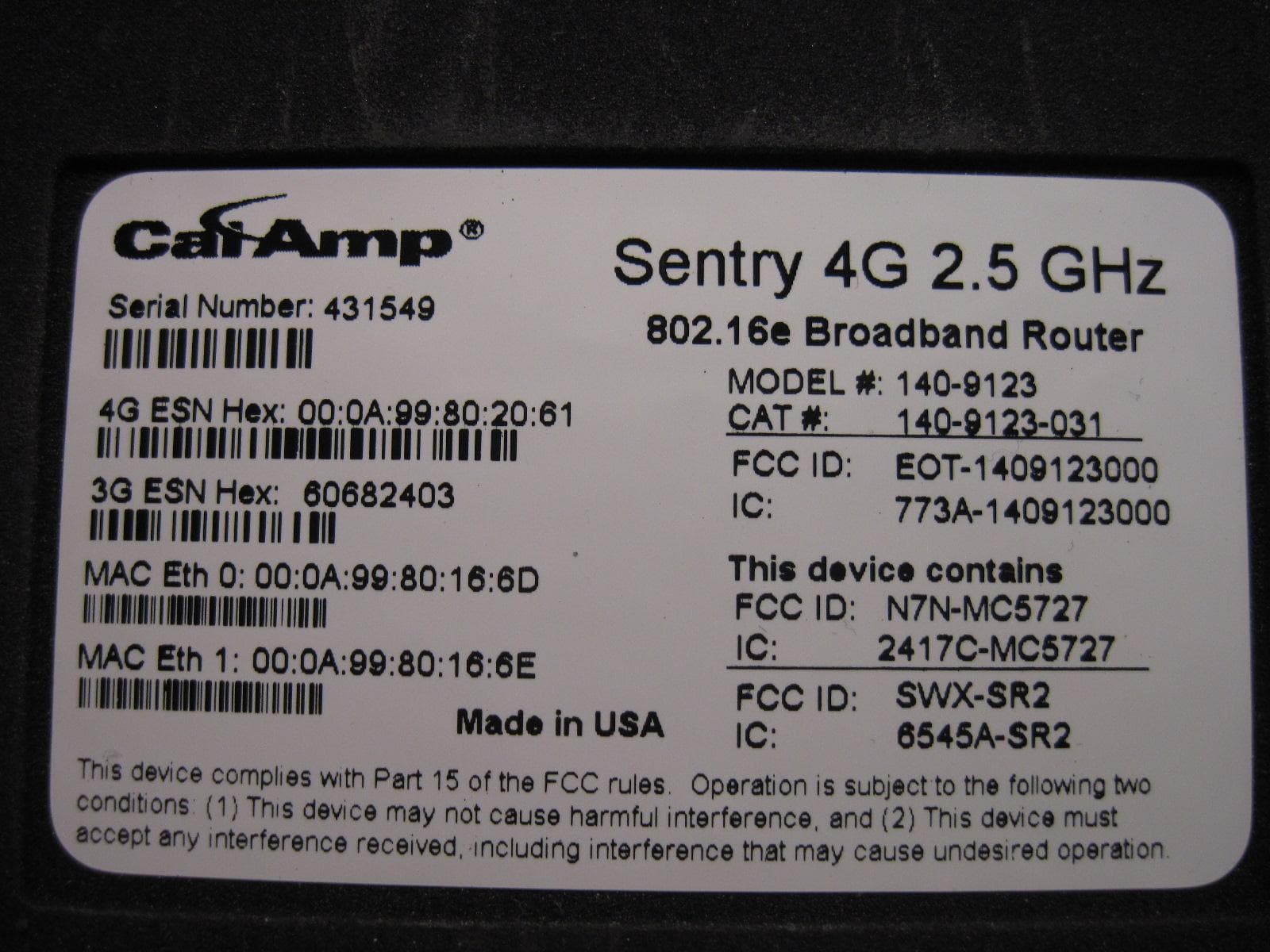
EOT-1409123000
May 15, 20112.5 GHz Wireless Broadband Route
Equipment Class
TNB - Licensed Non-Broadcast Station Transmitter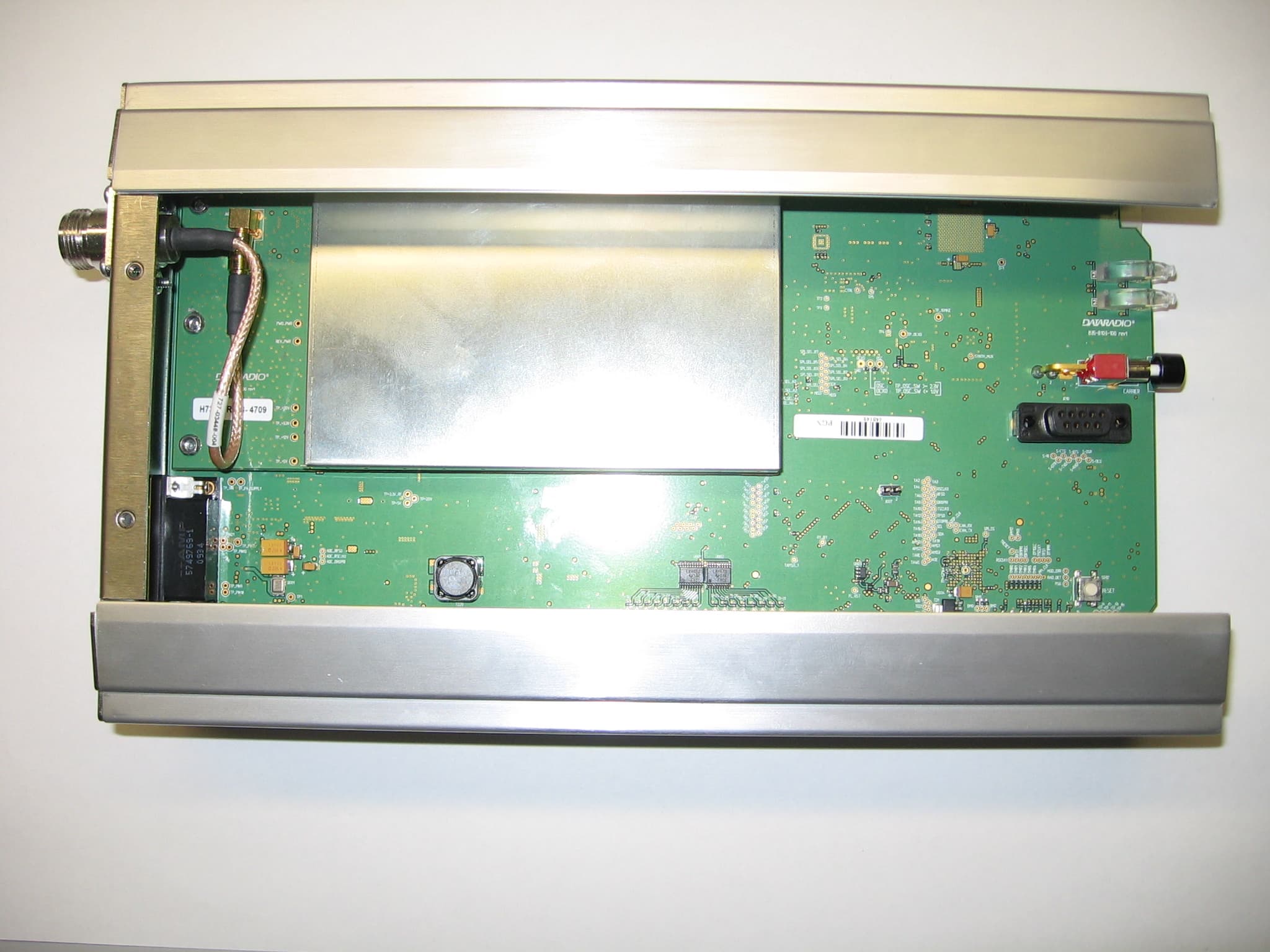
EOTBDP4-EXCT769
Sep 29, 2010700MHz Band SDR Exciter for BDP4 digital base station
Equipment Class
TNB - Licensed Non-Broadcast Station Transmitter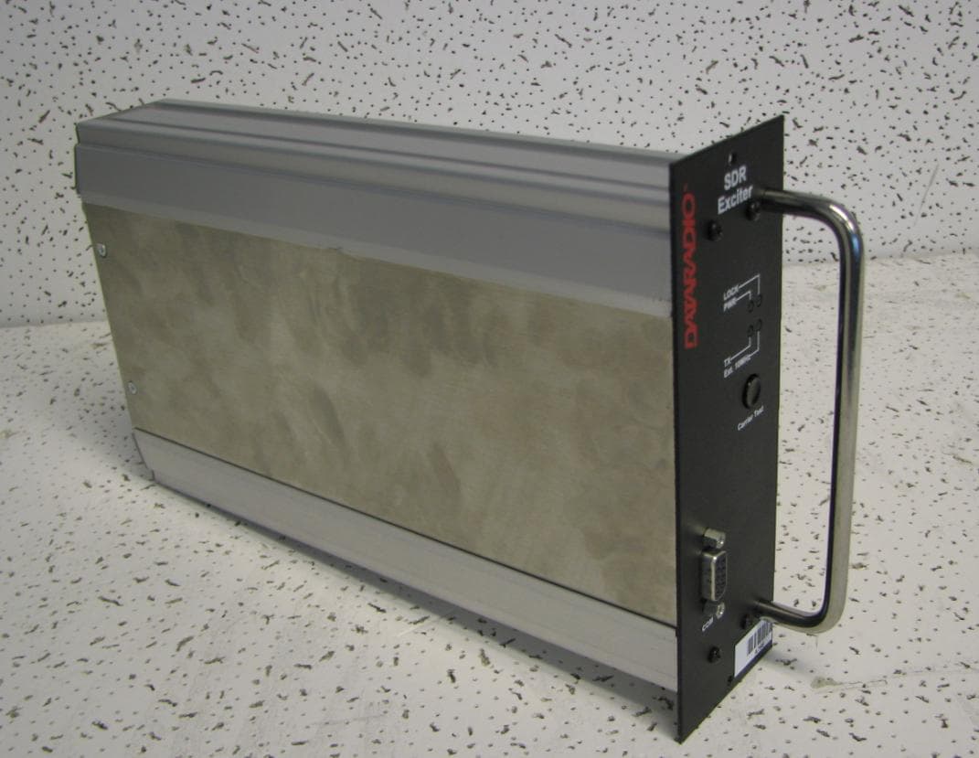
EOTBDP4-EXCT438
Jun 03, 2010UHF HIGH SDR Exciter for BDP4 digital base station
Equipment Class
TNB - Licensed Non-Broadcast Station Transmitter
EOTBDP4-EXCT403
Jun 02, 2010UHF LOW SDR Exciter for BDP4 digital base station
Equipment Class
TNB - Licensed Non-Broadcast Station Transmitter
EOT-1409290100
May 09, 2010900 MHz Broadband Base Station
Equipment Class
DTS - Digital Transmission System