EOTMCUB5R
CALAMP WIRELESS NETWORKS INC.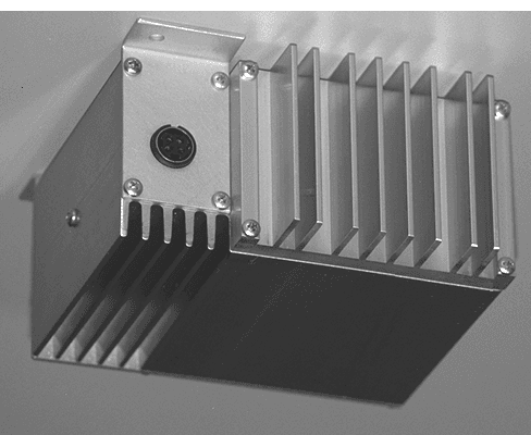
Click to zoom
Application Details
- Equipment Class
- TNB - Licensed Non-Broadcast Station Transmitter
- Date of Grant
- Jun 13, 1999
- Application Purpose
- Original Equipment
- Date of Application
- Apr 15, 1999
- Frequency Range
- 403.00000000 - 512.00000000
- Country
- United States
Documents & Files
Document Text
Text extracted from the exhibit documents filed with the FCC. Open a document above to read the original.
Users Manual
Integra-TR Technical Manual Version 0.02 PRELIMINARY The entire contents of this manual and the Software described in this manual are copyright 1999 by Dataradio Inc. Copyright D ATARADIO Inc. February 1999 Part no.: 120 4010x-002 i Table of Contents 1.PRODUCT OVERVIEW................................................................................................................................... 1 1.1 I NTENDED A UDIENCE ....................................................................................................................................... 1 1.2 G ENERAL D ESCRIPTION .................................................................................................................................... 1 1.2.1Characteristics ........................................................................................................................................ 1 1.2.2Accessories and options .......................................................................................................................... 1 1.3 C ONFIGURATION ............................................................................................................................................... 1 1.4 F ACTORY T ECHNICAL S UPPORT ........................................................................................................................ 2 1.5 P RODUCT W ARRANTY ...................................................................................................................................... 2 1.6 R EPLACEMENT P ARTS ....................................................................................................................................... 2 1.6.1Factory Repair ........................................................................................................................................ 2 1.7 P HYSICAL D ESCRIPTION .................................................................................................................................... 2 1.8 D IAGNOSTICS .................................................................................................................................................... 2 1.8.1Remote Commands.................................................................................................................................. 3 1.9 F IRMWARE U PGRADES ...................................................................................................................................... 3 1.10N ETWORK A PPLICATION ...............................................................................................................................3 1.10.1RF Path and Communications Range................................................................................................. 3 1.10.2Basic Connections .............................................................................................................................. 3 1.10.3 Common Characteristics ................................................................................................................... 3 1.10.4Point to Point System.......................................................................................................................... 3 1.10.5Point–Multipoint System..................................................................................................................... 4 1.10.6Extending a Landline (Tail Circuit).................................................................................................... 4 2.FEATURES AND OPERATION ...................................................................................................................... 5 2.1 O VERVIEW ........................................................................................................................................................ 5 2.2 I NTENDED A UDIENCE ....................................................................................................................................... 5 2.3 F RONT P ANEL ................................................................................................................................................... 5 2.3.1Antenna Connector ................................................................................................................................. 5 2.3.2LED Indicators........................................................................................................................................ 5 2.3.3Connection to DTE.................................................................................................................................. 5 2.3.4Com Port ................................................................................................................................................. 6 2.3.5Setup Port................................................................................................................................................ 6 2.4 R EAR P ANEL ..................................................................................................................................................... 7 2.4.1Heat Sink ................................................................................................................................................. 7 2.4.2Power / Analog connector....................................................................................................................... 7 2.5 O PERATION ....................................................................................................................................................... 7 2.5.1Operating Modes..................................................................................................................................... 8 2.5.2Data Forwarding Timer .......................................................................................................................... 8 2.5.3Sending Break Signals ...................................................…
Text truncated - open the document above for the full version.
External Photos
MCUB5R - ENGINEERING REPORT-Annex C Page 1 of 3 04\16\99 1. External views.front view MCUB5R - ENGINEERING REPORT-Annex C Page 2 of 3 156-90002-100 Dataradio FCC submission top- right side view MCUB5R - ENGINEERING REPORT-Annex C Page 3 of 3 156-90002-100 Dataradio FCC submission rear-left view (BW)
ID Label/Location Info
1. Label identification and place : right side, the closest lateral side from antenna connector.
Internal Photos
1. Internal Photosassembly internal top-bottom view. mid-internal views
Operational Description
MCUB5R - ENGINEERING REPORT-Annex APage 1 of 14 04\16\99 156-90002-100 Dataradio FCC submission Annex A:Operational Description of Circuitry RULE PART NUMBER:2.1033 (c)(10) 1PURPOSE This report has been prepared to support the application for FCC Certification Per Code Of Federal Regulations, Title 47, Parts 2 And 90 for the MCUB5R radio-modem comprised of the JDT Model 242- 3412-xxx Transceiver and Dataradio 210-3315-xxx Modem. The report presents necessary information concerning electrical circuit description, measured performance and physical construction and configuration. Also parts 4 and 5 present active circuit devices functions for Transceiver and, accordingly, for Modem. 2.0DL-3412 TRANSCEIVER The main subassemblies of this transceiver are the RF board, VCO board, TCXO and modem assembly. A block diagram of the transceiver is located in Figure 2. The VCO board is enclosed by a metal shield and soldered directly to the RF board. The VCO is not serviceable. The DL3412 is available with a reference oscillator stability of ±1.5 PPM. The 17.5 MHz TCXO (Temperature Compensated Crystal Oscillator) is soldered directly to the RF board. The TCXO is not serviceable. 2.1SYNTHESIZER As stated previously, the synthesized output signal is produced by a VCO (voltage controlled oscillator). The VCO frequency is controlled by a DC voltage produced by the phase detector in U801. The phase detector senses the phase and frequency of the two input signals and causes the VCO control voltage to increase or decrease if they are not the same. The VCO is then "locked" on frequency. Programming of the synthesizer provides the data necessary for the internal prescaler and counters. One input signal is the reference frequency. This frequency is produced by the 17.5 MHz reference oscillator (TCXO). The other input signal is the VCO frequency. VOLTAGE-CONTROLLED OSCILLATOR Oscillator (Q850) The VCO is formed by Q850, several capacitors and varactor diodes, and ceramic resonator Z850. It oscillates at the transmit frequency in transmit mode and first injection frequency in the receive mode ( 403-512 MHz in transmit and 455.95-564.95 MHz in receive). Biasing of Q850 is provided by R862, R867 and R865. An AC voltage divider formed by C861, C862 and C859 initiates and maintains oscillation and also matches Q850 to the tank circuit ceramic resonator Z850 is grounded at one end to provide shunt inductance to the tank circuit. FREQUENCY CONTROL AND MODULATION The VCO frequency is controlled in part by DC voltage across varactor diodes CR851, CR854, CR855 and CR856. As voltage across a reverse-biased varactor diode increases, its capacitance decreases. Therefore, VCO frequency increases as the control voltage increases. CR851/CR856 and CR854/CR855 are paralleled varactors to divide the capacitance and improve linearity. The varactors CR851/CR854 are MCUB5R - ENGINEERING REPORT-Annex APage 2 of 14 156-90002-100 Dataradio FCC submission biased at -2.0V so the control line voltage can operate closer to ground. The control line is isolated from tank circuit RF by choke L851/L854. The amount of frequency change produced by CR851/CR854/CR855/CR856 is controlled by series capacitor C859. The -2.0V applied to the VCO is derived from the 17.5 MHz TCXO frequency that is amplified by Q701, rectified by CR701 and filtered by C705, C706, C707 and C708 on the RF board. The VCO frequency is modulated using a similar method. The transmit audio/data signal from J201, pin 6 is applied across varactor diode CR852 which varies the VCO frequency at an audio rate. Series capacitors C856/C870 set the amount of deviation produced along with CR853 and C858. R854 provides a DC ground on the anodes of CR852/CR853, and isolation is provided by R852 and C855. The DC voltage across CR853 provides compensation to keep modulation relatively flat over the entire bandwidth of the VCO. This compensation is required because modulation tends to increase as the VCO frequency gets higher (capacitance of CR854/CR855/CR856/CR851 gets lower). CR853 also balances the modulation signals applied to the VCO and TCXO. The DC voltage applied across CR853 comes from the modulation adjust control R827 on the RF board. R826 applies a DC biasing voltage to CR852. C821 provides DC blocking. RF isolation is provided by C858, R853 and R847. VCO AND REFERENCE OSCILLATOR MODULATION Both the VCO and reference oscillator (TCXO) are modulated in order to achieve the required frequency response. If only the VCO was modulated, the phase detector in U801 would sense the frequency change and increase or decrease the VCO control voltage to counteract the change (especially at the lower audio frequencies). If only the reference oscillator frequency is modulated, the VCO frequency would not change fast enough (especially at the higher audio frequencies). Modulating both VCO and reference oscillators produces a flat audio response. Potentiometer R827 sets the VCO modulation sensitivity so that it is equal to the reference oscillator modulation sensitivity. CASCODE AMPLIFIERS (Q851/Q852) The output signal on the collector of Q850 is coupled by L861/C864 to buffer amplifier Q851/Q852. This is a shared-bias amplifier which provides amplification and also isolation between the VCO and the stages which follow. The signal is direct coupled from the collector of Q852 to the emitter of Q851. The resistors in this circuit provide biasing and stabilization, and C865 and C866 are bypass capacitors. AMPLIFIER (Q853) Amplifier Q853 provides amplification and isolation between the VCO and receiver, and transmitter. C868 provides matching between the amplifiers. Bias for Q853 is provided by R871, R872 and R874. Inductor L856 and capacitor C873 provide impedance matching on the output. VOLTAGE FILTER (Q901) Q901 on the RF board is a capacitance multiplier to provide filtering of the 4.6V supply to the VCO. R901 provides transistor bias and C901 provides the capacitance that is multiplied. If a n…
Text truncated - open the document above for the full version.
Parts List/Tune Up Info
9. Tune-up procedure Ref: FCC Part 2 paragraph 2. 1033(c)(9) 1. Connect the transceiver to be aligned to a DC power source. A DC current meter capable of measuring at least 2.5 Amps should be connect in line with the DC source. Connect the output of the transceiver through a watt meter and into a 50 ohm dummy load. 2. Load the synthesizer with the center channel frequency. 3. Key the transmitter and make certain that the supply voltage at the RF board is 13.3 VDC. (Do not transmit for extended periods of time. ) 4. Adjust R535 clockwise for 5.0 Watts of output power. 5. Check the power levels on the low and the high frequencies for 5.0 Watts +/- 1 Watt. 4. DL-3412 ACTIVE CIRCUITS DESCRIPTION DesignatorFunctionJEDEC or Vendor Type CR561Antenna switchMMBV3401 CR562Antenna switchMMBV3401 CR591Directional couplerMMBD701LT1 CR592Directional couplerMMBD701LT1 CR701RectifierBAV99LT1 CR851VaractorBB535E7908 CR852VaractorBB515 CR853Deviation level biasBB515 CR854VaractorBB535E7908 CR855VaractorBB535E7908 CR856VaractorBB535E7908 CR901VaractorBB535E7908 Q101Tx enableMUN5213T1 Q102Tx enableMUN5114T1 Q121Rx enableMUN5213T1 Q122Rx enableMUN5213T1 Q123Rx enableMUN2114T1 Q124Soft key up controlPZT2222AT1 Q1315 volt shutdownMUN5213T1 Q171Pin shiftMUN5213T1 Q172Pin shiftMUN2114T1 Q501RF bufferMSA-2111 Q511RF driverNE85633 Q531Power controlPZT2222AT1 Q701AmplifierMMBT918LT1 Q801Constant voltage sourceMDS1819A-RT1 Q841Pin ShiftMUN5231T1 Q842Pins shiftMUN5114T1 Q850VCONE85619 Q851Cascode ampNE85619 Q852Cascode ampNE85619 Q853AmplifierNE85619 Q901Capacitance multiplierMDS1819A-RT1 U111ASoft key up controlLMC660AIM U111BSoft key up controlLMC660AIM U111CPower controlLMC660AIM U111DSoft key up controlLMC660AIM U131Voltage regulatorTK11900MTL U141Voltage regulatorTK11900MTL U581AV-fwd ampMC33172DT U581BV-rev ampMC33172DT U811SynthesizerSA7025DK-T U521RF power moduleM57721M 5.INTEGRA R 210-3315-XXX ACTIVE CIRCUITS DESCRIPTION DesignatorfunctionType D1DIODE, HOT CARRIER, SOT-23MMBD301LT1 D2DIODE, HOT CARRIER, SOT-23MMBD301LT1 D3DIODE, SOT-23BAV99LT1 D4DIODE, SOT-23BAV99LT1 D5DIODE, SOT-23BAV99LT1 D6DIODE,RECTF,1A/100V1N4001 DS1LED,3MM,BICOLOR,RED/GREEN SMT591-3001-102 DS2LED,3MM,BICOLOR,RED/GREEN SMT591-3001-102 DS3LED,3MM,BICOLOR,RED/GREEN SMT591-3001-102 DS4LED,3MM,BICOLOR,RED/GREEN SMT591-3001-102 Q1TRANSISTOR, GENERAL PURPOSE,SOT-23MMBT3904LT1 Q2TRANSISTOR, GENERAL PURPOSE,SOT-23MMBT3904LT1 Q3TRANSISTOR, GENERAL PURPOSE,SOT-23MMBT3904LT1 Q4TRANSISTOR, GENERAL PURPOSE,SOT-23MMBT3904LT1 U1QUAD, OP-AMP , -40/+85 SO-14TLC2274ID U2HEX INVERTER CMOS74HC04AD U3QUAD OP-AMPLMC6484AIM U48 BIT A/D,-40/+85C SO-20WADC0838CIWM U5POTENTIOMETER 4 DIGITALAD8403AR50 U6TEMPERATURE SENSOR,SOT-23LM50CIM3 U7DUAL OP-AMP,-40/+85 S0-8TLC2272ID U8ANALOG MULTIPLEXERS/DEMULTIPLEXERS SOIC 16 MC74HC4053D U9QUAD, OP-AMP , -40/+85 SO-14TLC2274ID U10FILTER, LINEAR PHASE LOW PASS S0-8LTC1069-7 U11REGULATOR,MICROPOWER VOLTAGE ,S0-8LP2951CD U12REGULATOR,LOW DROPOUT,Q PACKAGELT1129IQ-5 U13DUAL MONOSTABLE, SOIC74HC4538AD U14QUAD NAND GATE74HC00AD U15CONVERTER RS-232ADM223AR U16 ( TO BE PROGRAMMED ) CPLD 64 MACROCELLPZ5064-I12A44 U17MICROPROCESSOR ,10MHzZ8401510FEC U18RAM,CMOS,32K x 8, -40/=85, SOP-28TC55257DFI-85L or TC55257DFL-85L (SCREENED -40 +85) U19RESET CIRCUIT, -40+85 ,S0-8MC33064D-5 U20HEX OR GATE,CMOS74VHC32AD U21MICROPROCESSOR ,10MHzZ84C1510FEC /Z8401510FEC U22 ( TO BE PROGRAMMED ) EPROM, FLASH 1 MEGABIT, -40/+85 PLCCAT29C010A-90J1 X1XTAL, FPX SERIES 19.6608 MHzFPX196-20PF
Schematics
MCUB5R - ENGINEERING REPORT-Annex B Page 1 of 6 04\16\99 156-90002-100 Dataradio FCC submission Annex B: SchematicsRULE PART NUMBER: 2.1033 (c)(10) ContentsIntegra R Modem/loader ............................pag 2-5DL3412 Transceiver...................................pag 6 MCUB5R - ENGINEERING REPORT-Annex B Page 2 of 6 156-90002-100 Dataradio FCC submission 78 U22AT29C010 A0 12 A1 11 A2 10 A3 9 A4 8 A5 7 A6 6 A7 5 A8 27 A9 26 A10 23 A11 25 A12 4 A13 28 A14 29 CE 22 OE 24 O0 13 O1 14 O2 15 O3 17 O4 18 O5 19 O6 20 O7 21 - 1 A16 2 VCC 32 A15 3 WE 31 - 30 GND 16 U20A 74VHC32 12 3 U2B 74VHC04 34 C5633PF C60 33PF R78 10K R77 100K C62104 R75 47K U19 MC33064D-5 RST 1 IN 2 GND 4 U1784015 A0 6 A1 5 A2 4 A3 3 A4 2 A5 1 A6 100 A7 99 A8 98 A9 97 A10 96 A11 95 A12 94 A13 93 A14 92 A15 91 D0 89 D1 88 D2 87 D3 86 D4 85 D5 84 D6 83 D7 82 PA0 29 PA1 28 PA2 27 PA3 26 PA4 25 PA5 24 PA6 23 PA7 22 PB0 53 PB1 54 PB2 55 PB3 56 PB4 57 PB5 58 PB6 59 PB7 60 W/RDYA 30 SYNA 31 RXDA 32 RXCA 33 TXCA 34 TXDA 35 DTRA 36 RTSA 37 CTSA 38 DCDA 39 W/RDYB 52 SYNCB 51 RXDB 50 RXCB 49 TXCB 48 TXDB 47 DTRB 46 RTSB 45 CTSB 44 DCDB 43 WDOUT 73 A7RF 70 ICT 40 ICT 42 RFSH 7 M1 8 RST 9 BSREQ 10 WAIT 11 BUSACK 12 WR 13 RD 14 IORQ 15 MREQ 17 HALT 18 INT 19 NMI 63 EV 67 XTAL1 65 XTAL2 66 CKOUT 68 CKIN 69 ARDY 20 ASTB 21 BRDY 62 BSTB 61 CK0 81 CK1 80 CK2 79 CK3 78 TO0 74 TO1 75 TO2 76 TO3 77 IEO 71 IEI 72 5V 41 5V 90 GND 16 GND 64 U18 55C256 A0 10 A1 9 A2 8 A3 7 A4 6 A5 5 A6 4 A7 3 A8 25 A9 24 A10 21 A11 23 A12 2 A13 26 A14 1 CE 20 OE 22 WE 27 O0 11 O1 12 O2 13 O3 15 O4 16 O5 17 O6 18 O7 19 VCC 28 GND 14 R76 47K P1 HEADER 8 12345678 R73 100K R80 100K R81 100K R79 100K R74 470K U2F 74VHC04 13 12 X1 19.6608MHZ 14 U16 PZ5064_PLCC 332-90804-000 PLL_LOCK 37 NC 1 NC 5 A 33 B 32 NC 44 PREAMB 36 INV 34 SCRAM_EN 24 TXD 25 NC 8 NC 7 NC 9 CK128 4 RXS 31 RX_EN 20 NC 2 NC 6 DATA_CK 21 RXD 28 TXA 29 SLICER 17 FILTER_CK 18 EDGE 40 VDD 15 VDD 23 VDD 35 VDD 3 GND 10 GND 22 GND 30 GND 42 NC 11 CK0 19 CK 43 NC 41 RXC 27 TXC 26 GMSK 39 NC 16 NC 14 NC 13 NC 38 NC 12 U20B 74VHC32 45 6 U2184015 OR 84C15 A0 6 A1 5 A2 4 A3 3 A4 2 A5 1 A6 100 A7 99 A8 98 A9 97 A10 96 A11 95 A12 94 A13 93 A14 92 A15 91 D0 89 D1 88 D2 87 D3 86 D4 85 D5 84 D6 83 D7 82 PA0 29 PA1 28 PA2 27 PA3 26 PA4 25 PA5 24 PA6 23 PA7 22 PB0 53 PB1 54 PB2 55 PB3 56 PB4 57 PB5 58 PB6 59 PB7 60 W/RDYA 30 SYNA 31 RXDA 32 RXCA 33 TXCA 34 TXDA 35 DTRA 36 RTSA 37 CTSA 38 DCDA 39 W/RDYB 52 SYNCB 51 RXDB 50 RXCB 49 TXCB 48 TXDB 47 DTRB 46 RTSB 45 CTSB 44 DCDB 43 WDOUT 73 A7RF 70 CSO 40 CSI 42 RFSH 7 M1 8 RST 9 BSREQ 10 WAIT 11 BUSACK 12 WR 13 RD 14 IORQ 15 MREQ 17 HALT 18 INT 19 NMI 63 EV 67 XTAL1 65 XTAL2 66 CKOUT 68 CKIN 69 ARDY 20 ASTB 21 BRDY 62 BSTB 61 CK0 81 CK1 80 CK2 79 CK3 78 TO0 74 TO1 75 TO2 76 TO3 77 IEO 71 IEI 72 5V 41 5V 90 GND 16 GND 64 TP3TP4TP2 D6 A1 D4 A5 A13 A3 A2 D0 A4 A11 D5 A1 A1 A14 D4 D3 D5 A9 A3 D5 D3D7 A12 A7 A10 A3 D2 D4 D5 A4 A1 A8 D1 D0 D0 A11 A6 A9 A2 A0 A7 A3 D7 D2 A8 A6 A12 A4 A10 D7 A6 A9 D6D1 A13A5 A0 A0 D6 A8 A5 D4 D2 D1 A13 A5 A12 A14 A14 D7D2 A6 A2A7 D3 A11 A2 D3 A7 D6 A0 D1 A4A10 D0 \A7 +5V +5V +5V +5V +5V +5V +5V +5V +5V +5V +5V +5V +5V +5V +5V +5V LOCK LED-1LED-2LED-3LED-4LED-5LED-6LED-7LED-8 RXD-2 TXD-2DCD-2 OUT1OUT2 A/D-OUTPUT A/D-SELECTFAST_PEAK_DETECT TXD-1DTR-1 RX-CNT CD DCD-1 \NMI \SLEEPCLOCK SYNTH_ENABLE RADIO-CLOCKTP-CNT RXD-1 DATA RTS-1 CTS-1 RS232-CNTDIGIPOT_SELECT RX_EN1 TX_EN1DIAG_ENABLERADIO-DATA RXS FILTER_CKSLICERTXA_MOD \M1 \RST \IORQ CKIN \INT PREAMB \M1 \RST \IORQ \INT CKIN CK0 IEO \MREQ \MREQ INV A CKIN B IEO PREAMBINVAB CK0 CK0 PLL_LOCK PLL_LOCK GMSK GMSK \RD \WR \RD\WR REV DESCRIPTION DATE DATARADIO INC. DraftDesignDesign P/N SIZE B SHEET CheckDOC/N REV DATE No reproduction or distributionwithout approval.This information is the property ofDATARADIO INC. and is confidentialNOTES: (Unless otherwise specified) 12345 ABCDEF GH 1235 ABCDEF GH LEVEL C.LAMBERTD.NGUYEN 1/4 INTEGRA - RLOGIC BOARD 1 PRODUCTION 981111 (3) (2) (4) (4)(4) (4) (4) (2,4)(3)(4) (3) (2) (3)(3)(3)(3)(3)(3)(3)(3) (3) (3) (3) (2,4)(2,4)(4) (3) (3)(3)(3) (3) (3) CTS-3+5VDTR-3 RXD-3 RTS-3 TXD-3DCD-3 GND (4) (4) (4)(4) (4)(4) COPYRIGHT C 1985-97 : DATARADIO INC. (2) 981111 (2)(2)(2) 4 215-03315-001 MCUB5R - ENGINEERING REPORT-Annex B Page 3 of 6 156-90002-100 Dataradio FCC submission R24 6.8K U5E AD8403_50K AGND1 21 AGND2 1 AGND3 17 AGND4 5 DGND 9 VDD 16 RS 15 SHDN 10 SDI 12 CLK 14 CS 11 SDO 13 R54 1K U1C TLC2274 10 9 8 - + U3D LMC6484 1213 14 -+ U3C LMC6484 10 9 8 -+ U1D TLC2274 1213 14 4 11 - + +- D1 MBD301 13 Q2 MMBT3904 3 1 2 Q1 MMBT3904 3 1 2 U9D TLC2274 1213 14 -+ U9A TLC2274 32 1 -+ C34 224 35V_A + R17 10K R27 10K R22 470K R968K R710K R8 470K R58 100K R61 100K R10220K C7 104 R33 220K TP1 C8 224 35V_A + C29 104 C28 102 R6 10K U3B LMC6484 56 7 -+ C5 103 U1B TLC2274 56 7 -+ R2 10K R410K R13 220K R16470K R12 470K U1A TLC2274 32 1 -+ C25 102 R14 68K U8A74HC4053D X0 12 X1 13 A 11 X 14 R32 220K U10 LTC1069-7 GND 1 V+ 2 VIN 4 CLK 5 V- 7 VOUT 8 GND 3 GND 6 R53 1K R1118K U9B TLC2274 56 7 4 11 - + +- U3A LMC6484 32 1 4 11 - + +- U5DAD8403_50K 7 8 6 B4 A4 W4 C9 220PF U5CAD8403_50K 20 18 19 B3 A3 W3 U5B AD8403_50K 3 4 2 B2 W2 A2 C23 470PF U8B74HC4053D Y0 2 Y1 1 B 10 Y 15 D2 MBD301 13 C1 224 35V_A + R18 10K R28 10K R48 10K R49 10K R110K +5V_SW +2.5V +5V_SW +2.5V +5V_SW +5V_SW +2.5V +5V_SW +2.5V +2.5V +2.5V +2.5V +5V_SW +2.5V +5V_SW +5V_SW +5V_SW +5V_SW +2.5V RXA FAST_PEAK_DETECT NEG_PEAK RX_TP POS_PEAK RXS SLICER TXA_MOD FILTER_CK DATA CLOCK DIGIPOT_SELECT TXA TX_EN1 REV DESCRIPTION DATE DATARADIO INC. DraftDesign P/N SIZE B CheckDOC/N DATE No reproduction or distributionwithout approval.This information is the property ofDATARADIO INC. and is confidential 12345 ABCDEFGH 12345 ABCDEFGH LEVEL COPYRIGHT C 1985-97 : DATARADIO INC. INTEGRA - R 2/4 Design D.NGUYEN 1 PRODUCTION 981111 (1) (3) (4) (4) (1) (1) (1) (1) (1) (1) (1) (1) SHEET (4) (4) 981111 215-03315-001 C.LAMBERT MCUB5R - ENGINEERING REPORT-Annex B Page 4 of 6 156-90002-100 Dataradio FCC submission U14B 74HC00 45 6 U14C 74HC…
Text truncated - open the document above for the full version.
Test Report
Engineering Report in Support of Certification FCC Form 731 for MCUB5R radiomodem Subject:Compliance of Radio Modem with Respect to FCC Rules & Regulations Parts 2 and 90 Certification FCC Form 731 Equipment:UHF Radio Modem FCC Id:EOTMCUB5R Applicant:Dataradio Inc. 5500 Royal Mount Ave., Suite 200 Town of Mount Royal, H4P 1H7 Quebec, Canada April 16, 1999 Dataradio Inc MCUB5R - ENGINEERING REPORT-bodyPage 2 of 43 156-90002-100 Dataradio FCC submission Johnson Data Telemetry Corporation Waseca, Minnesota ENGINEERING STATEMENT OF MARK CHRISTENSEN The application consisting of the attached engineering exhibit and associated FCC form 731, has been prepared in support of a request for Type Acceptance for the Johnson Data Telemetry (JDT) DL-3412, 403-512 MHz Transceiver with the Data Radio 3315(Integra) Modem. The Transceiver mated with the Integra Modem will be identified by the part number INA12XY0T where X represents range and Y represents IF bandwidth (see below for part#). The model name is MCUB5R. The Transceiver/Modem will be identified by the FCC number EOTMCUB5R. The transceiver operates pursuant to Part(s) 90 and 15 of the Rules and Regulations. EXISTING CONDITIONS The units utilized for these type acceptance measurements were obtained from the pilot-production. The transceiver is designed to operate on frequencies ranging from 403.000 MHz to 512.000 MHz. The frequency tolerance of the transceiver is .00015% or 1.5 parts per million. The frequency stability of the transceiver is controlled by a temperature compensated crystal oscillator (TCXO) operating at 17.5 MHz. PROPOSED CONDITIONS It is proposed to Type Accept the MCUB5R, 403-512 MHz Transceiver/Modem for operation in the band of frequencies previously outlined. The applicant anticipates marketing the device for use in wireless transmission of data. PERFORMANCE MEASUREMENTS All Type Acceptance measurements were conducted in accordance with the Rules and Regulations Section 2.1041of Pike & Fischer Inc., CD ROM revision 9/28/98. Equipment performance measurements were made in the engineering laboratory and on the FCC certified Open Area Test Site at the Transcrypt International / E.F. Johnson Radio Products located at 299 Johnson Avenue in Waseca, Minnesota. All measurements were made and recorded by myself or under my direction. The performance measurements were made between Jan 28, 1999 and Feb 8,1999. CONCLUSION Given the results of the measurements contained herein, the applicant requests that Type Acceptance be granted for the INA12XY0T, 403-512 MHz Transceiver/Modem as tested for data communications. 4/5/99 Mark Christensen Director of Engineering, Johnson Data Telemetry Part Number X Freq Range Y IF Bandwidth 1380-403 MHz112.5 KHz 2403-419 MHz325 KHz 3419-435 MHz 4435-451 MHz 5450-470 MHz 6464-480 MHz 7480-496 MHz 8496-512 MHz MCUB5R - ENGINEERING REPORT-bodyPage 3 of 43 156-90002-100 Dataradio FCC submission QUALIFICATIONS OF ENGINEERING PERSONNEL (2.911) NAME:Allen Frederick TITLE:Certified Technologist TECHNICAL EDUCATION:Bachelor of Science Degree in Electronic Engineering Technology (1998) from Mankato State University TECHNICAL EXPERIENCE:2 years experience in analog and radio frequency communications NAME:Constantin Pintilei TITLE:R&D Test Engineer TECHNICAL EDUCATION: Bachelor of Science Degree in Radiotechnique Electronic Engineering (1993) from Technical University of Iasi, Romania TECHNICAL EXPERIENCE:5 years experience in radio frequency measurements MCUB5R - ENGINEERING REPORT-bodyPage 4 of 43 156-90002-100 Dataradio FCC submission Contents CONTENTS ......................................................................................................................................................4 ENGINEERING SUMMARY.........................................................................................................................5 GENERAL INFORMATION .........................................................................................................................6 FCC SUBMISSION INFORMATION .....................................................................................................................6 M ANUFACTURER ’ S DATA ................................................................................................................................6 P RODUCT ’ S GENERAL SPECIFICATIONS ............................................................................................................6 INFORMATION FOR CERTIFICATION ...................................................................................................7 1. Name of Applicant:.................................................................................................................................7 2. FCC Identifier ........................................................................................................................................7 3. Instruction book......................................................................................................................................7 4. Types of emission ...................................................................................................................................7 5. Frequency range ....................................................................................................................................7 6. Range of operating power levels ............................................................................................................7 7. Maximum Power rating.........................................................................................................................8 8. DC voltages and currents into final amplifier........................................................................................8 9. Tune-up procedure .................................................................................................................................8 10. Complete circuit diagram, circuitr…
Text truncated - open the document above for the full version.
Contact Information
Applicant
Russell Cook(Director of Engineer)
[email protected]612-642-2127
Technical Contact
Dataradio IncConstantin Pintilei
[email protected]514-737-0020
suite 200 · Mount-Royal, Quebec · Canada
Test Firm
E. F. Johnson Co.John Oblak
Technical Specifications
| # | Rule Parts | Frequency Range | Power Output | Emission | Tolerance |
|---|---|---|---|---|---|
| 2 | 90.21 | 403 MHz - 512 MHz | 5 W | 9K30F1D | 1.5 ppm |
Other Applications from CALAMP WIRELESS NETWORKS INC.
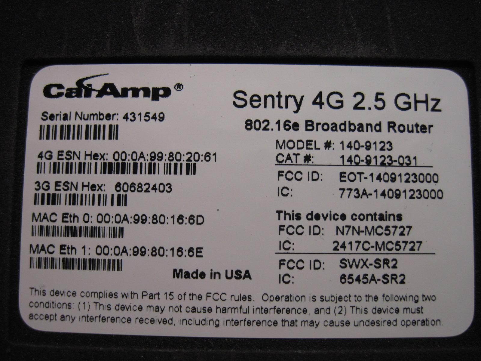
EOT-1409123000
May 15, 20112.5 GHz Wireless Broadband Route
Equipment Class
TNB - Licensed Non-Broadcast Station Transmitter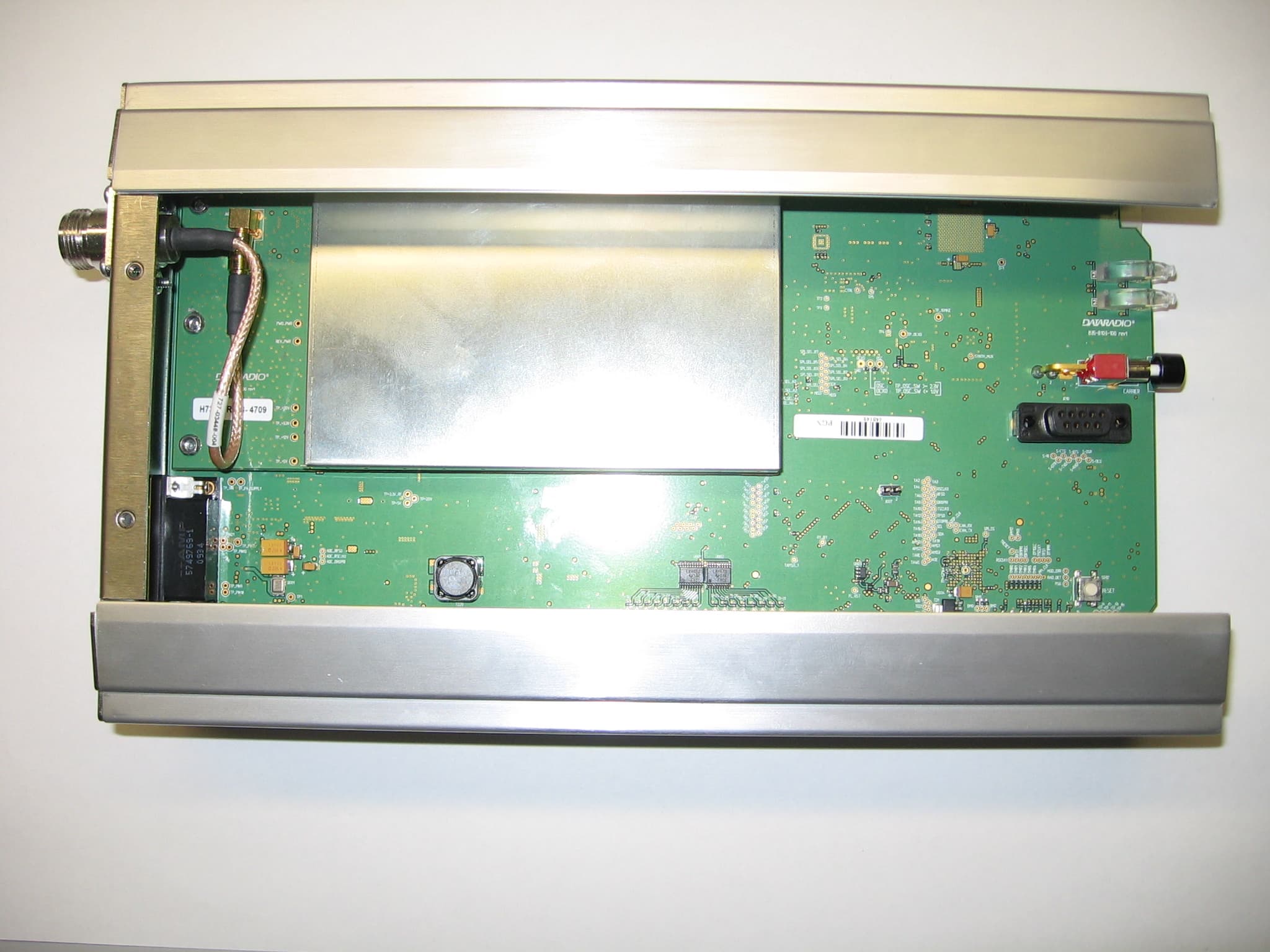
EOTBDP4-EXCT769
Sep 29, 2010700MHz Band SDR Exciter for BDP4 digital base station
Equipment Class
TNB - Licensed Non-Broadcast Station Transmitter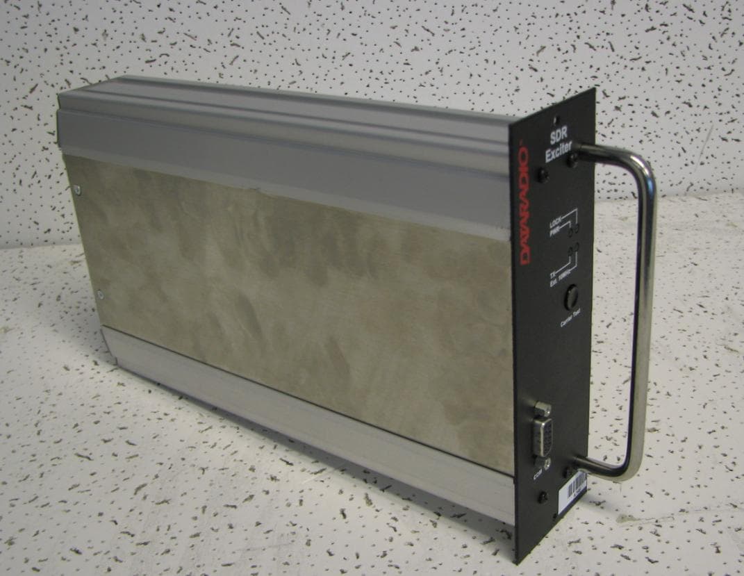
EOTBDP4-EXCT438
Jun 03, 2010UHF HIGH SDR Exciter for BDP4 digital base station
Equipment Class
TNB - Licensed Non-Broadcast Station Transmitter
EOTBDP4-EXCT403
Jun 02, 2010UHF LOW SDR Exciter for BDP4 digital base station
Equipment Class
TNB - Licensed Non-Broadcast Station Transmitter
EOT-1409290100
May 09, 2010900 MHz Broadband Base Station
Equipment Class
DTS - Digital Transmission System