FFMHG10ZZ0ENCXLUSSMART GATEWAY
LG Electronics, Inc.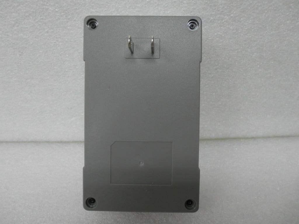
Click to zoom
Application Details
- Equipment Class
- DTS - Digital Transmission System
- Date of Grant
- Dec 12, 2012
- Application Purpose
- Original Equipment
- Date of Application
- Dec 12, 2012
- Equipment Note
- SMART GATEWAY
- Frequency Range
- 2422.00000000 - 2452.00000000
- Company
- LG Electronics, Inc.
- Country
- South Korea
Documents & Files
Document Text
Text extracted from the exhibit documents filed with the FCC. Open a document above to read the original.
Users Manual
IMPORTANT SAFETY INSTRUCTIONS READ ALL INSTRUCTIONS BEFORE USING THE APPLIANCE. Always comply with the following precautions to avoid dangerous situations and ensure peak performance of your product. WARNING It can result in serious injury or death when the directions are ignored. CAUTION It can result in minor injury or product damage when the directions are ignored WARNING Installation Do not install the product near a heat source. There is a risk of fire. Do not place the product where oil, steam, salt, Sulfuric acid occurs. There is a risk of fire or explosion. Do not install the product to concerns fall loosely. It may cause damage to the product. Or there is a risk of injuries caused by the crash of the product. Do not place the product in rainy place. There is a risk of fire or electric shock. Do not place the product in damp environment. There is a risk of fire or electric shock. Do not place the product near a heater or electric wire. There is a risk of fire. Do not place the product incoming direct sunlight. There is a risk of damage to the plastic parts of the product. Do not use improper rated voltage, current. There is a risk of fire or failure of product. Operation Take care to ensure that power cable could not be pulled out or damaged during operation. There is a risk of fire or electric shock. Make sure the power cord is plugged firmly and completely into the outlet. There is a risk of fire or failure of product. Do not modify or extend the power cable. There is a risk of fire or electric shock. ! ! ! Do not touch the product, power plug, LAN cable with a wet hand. There is a risk of electric shock. When the product is soaked (or flooded, submerged), contact an Authorized Service Center. There is a risk of fire or electric shock. If strange sounds, or odors, smoke comes from product. Turn the breaker off or disconnect the power supply cable. There is a risk of electric shock or fire. Do not place anything on the product. It may cause failure of product. Do not allow to use the product by young children or elderly infirm without administrator’s permission. It may cause injury or damage to the product. Do not share the outlet with other appliances. It may cause fire due to heat generation. Do not allow water to run or wet into electric parts. There is a risk of fire or electric shock. Turn the main power off when cleaning or maintaining the product. There is a risk of fire or electric shock. Do not use harsh detergents, solvents. There is a risk of fire or damage to the plastic parts of the product. Do not disassemble or modify products by yourself. There is a risk of fire, electric shock, explosion, or injury. Do not clean the product with wet clothes. There is a risk of fire or electric shock. Do not store or use flammable gas or combustibles near the product. There is a risk of fire or explosion. CAUTION Operation Provide sufficient protection against noise when installing the equipment such as telecom base stations of hospital, etc. Inverter equipment, private generators, high-frequency medical equipment, telecommunications can cause abnormal operation of malfunction of the product. On the other hand, product makes disturbance noise that can affect medical equipment or video broadcast. Do not install the product out-range of operating temperature. There is a risk of failure of product. Do not use external code conversion plug. There is a risk of failure of product. Do not smash the product. There is a risk of failure of product. ! Name of each part ※ Image of this manual may differ from the actual appearance. Function LED - POWER : When the power supplied, red light turns on. When it’s ready to operate, light turns to green. - Wi-Fi : When the power supplied, green light turns on. - Zigbee 1 : When the power supplied, green light turns on. It flash when communicate to Smart meter. - Zigbee 2 : When the power supplied, green light turns on. It flash when communicate to appliances. Reset button : Push reset button until WiFi LED turns off, network configuration is initialized. WPS button : It can help connect to router easily with Wi-Fi. Please refer to router’s manual for detailed explanation. LAN port : Connect to router or PC. Components Function LED WPS button LAN port Reset button User manual LAN Cable ※ Image of this manual may differ from the actual appearance. Install and ready to connect How to install Smart Gateway Connection setting with Wi-Fi 1 When power is supplied for Smart Gateway, ‘POWER’ LED turns to red. When it’s ready to operate, LED turns to green. 2 Connect to LG Smart Gateway with Wi-Fi of laptop or Smartphone. Please refer to manual of Smartphone or laptop for detailed explanation. 3 Enter the initial password ‘lgsmartgateway2012’. Connection setting with LAN cable 1 When power is supplied for Smart Gateway, ‘POWER’ LED turns to red. If it’s ready to operate, LED turns to green. 2 Plug the LAN cable to LAN port on the bottom of the Smart Gateway. And plug the other end to the PC’s LAN port. TROUBLESHOOTING Before requesting service Please check the following before you contact the service center. If the problem persists, contact your local service center. Problem Possible Causes What To Do Smart Gateway does not work. Smart Gateway is unplugged Voltage is lower than rated voltage. Make sure the Smart Gateway is pushed completely into the outlet. Check the rated voltage. LED light does not turns on. LED is covered by material. Remove material that covers LED. Appliances are not joined to list. Appliance has communication problem a number of appliances excess. Reconnect to Smart Gateway after minutes. Because appliances are joined to Appliances are not controlled. Distance between Smart Gateway and appliance is too far. Check the strength of signal and make narrow distance. After set network configuration, Smartphone can’t connect to Smart Gateway. POWER light turns to red. Wi-Fi light turns off.…
Text truncated - open the document above for the full version.
External Photos
CTK Co., Ltd. 386-1, Ho-dong, Cheoin-gu, Yongin-si, Gyeonggi-do, 449-100, Korea Tel: +82-31-339-9970 Fax: +82-31-339-9855 www.e-ctk.com EUT External Photographs CTK Co., Ltd. 386-1, Ho-dong, Cheoin-gu, Yongin-si, Gyeonggi-do, 449-100, Korea Tel: +82-31-339-9970 Fax: +82-31-339-9855 www.e-ctk.com
ID Label/Location Info
CTK Co., Ltd. 386-1, Ho-dong, Cheoin-gu, Yongin-si, Gyeonggi-do, 449-100, Korea Tel: +82-31-339-9970 Fax: +82-31-339-9855 www.e-ctk.com Label Photographs
Internal Photos
CTK Co., Ltd. 386-1, Ho-dong, Cheoin-gu, Yongin-si, Gyeonggi-do, 449-100, Korea Tel: +82-31-339-9970 Fax: +82-31-339-9855 www.e-ctk.com EUT Internal Photographs CTK Co., Ltd. 386-1, Ho-dong, Cheoin-gu, Yongin-si, Gyeonggi-do, 449-100, Korea Tel: +82-31-339-9970 Fax: +82-31-339-9855 www.e-ctk.com CTK Co., Ltd. 386-1, Ho-dong, Cheoin-gu, Yongin-si, Gyeonggi-do, 449-100, Korea Tel: +82-31-339-9970 Fax: +82-31-339-9855 www.e-ctk.com CTK Co., Ltd. 386-1, Ho-dong, Cheoin-gu, Yongin-si, Gyeonggi-do, 449-100, Korea Tel: +82-31-339-9970 Fax: +82-31-339-9855 www.e-ctk.com WLAN Antenna CTK Co., Ltd. 386-1, Ho-dong, Cheoin-gu, Yongin-si, Gyeonggi-do, 449-100, Korea Tel: +82-31-339-9970 Fax: +82-31-339-9855 www.e-ctk.com Zigbee Antenna 1 Zigbee Antenna 2
Operational Description
Integrated Antenna and RF Solutions 1 Product Specification AE020157-N Rufa 2.4 GHz SMD Antenna Part No. A5839 / A5887 Product Specification 1 Features • Designed for 2.4 GHz applications: Bluetooth ® , Wi-Fi ® (802.11b/g), ZigBee ® , etc. • Easy to integrate • Low profile design for use with no ground beneath the antenna • High efficiency • Light weight • Intended for SMD mounting • Supplied in tape on reel 2 Description Rufa is intended for use with all 2.4 GHz applications. The antenna uses a ground plane in order to radiate efficiently, but this ground plane must not extend underneath the antenna itself. The antenna is available in two versions with the feed locations on the right or left hand side of the antenna. 3 Applications • Mobile phones • PDAs • PNDs • Headsets • PMPs / MP3s • Laptops • PC-Cards • Sensors Rufa 2.4 GHz SMD Antenna Part No. A5839 / A5887 4 Part numbers Rufa Left: A5839 Rufa Right: A5887 150 5 General data Product name Rufa 2.4 GHz A5839 (Left) Part Number A5887 (Right) Frequency 2.4 – 2.5 GHz Polarization Linear Operating temperature -40 ºC to +85 ºC Impedance with matching 50 Ω Weight 0.1 g Antenna type SMD Dimensions 12.8 x 3.9 x 1.1 [mm] 6 Electrical characteristics Typical performanceConditions Peak gain 2.1 dBi Average gain -1.2 dBi Average efficiency 75% Maximum Return Loss -11 dB Maximum VSWR 1.8:1 All data measured on Antenova’s reference boards, part numbers A5839-U1 and A5887-U1 Data given for the 2.4 – 2.5 GHz frequency range Integrated Antenna and RF Solutions 2 Product Specification AE020157-N Rufa 2.4 GHz SMD Antenna Part No. A5839 / A5887 7 Electrical performance 7-1 Return Loss 2200 2300 2400250026002700 -40 -30 -20 -10 0 ∇ ∇ [MHz] [dB] 7-2 VSWR 2200 2300 2400250026002700 1 2 3 4 5 ∇ ∇ [MHz] Integrated Antenna and RF Solutions 3 Product Specification AE020157-N Rufa 2.4 GHz SMD Antenna Part No. A5839 / A5887 7-3 Antenna patterns Z X Y dBi 5 -35 -15 XZ plane ZY plane XY plane Patterns show combined polarisations measured on reference board A5839-U1 Integrated Antenna and RF Solutions 4 Product Specification AE020157-N Rufa 2.4 GHz SMD Antenna Part No. A5839 / A5887 8 Antenna dimensions Rufa Left Rufa Right L W H Length Width Height 12.8 ± 0.2 3.9 ± 0.2 1.1 ± 0.2 Dimensions in mm 9 Antenna footprint Rufa Left (Part No: A5839) Rufa Right (Part No: A5887) * CAD files of the antenna footprint are available from Antenova on request. Please contact [email protected] for further details. I S K J N L O 1.0 ± 0.12.0 ± 0.1 8.1 ± 0.13.7 ± 0.11.3 ± 0.12.4 ± 0.10.5 ± 0.1 Dimensions in mm Integrated Antenna and RF Solutions 5 Product Specification AE020157-N Rufa 2.4 GHz SMD Antenna Part No. A5839 / A5887 10 Electrical interface 10-1 Transmission lines • All transmission lines should be designed to have a characteristic impedance of 50 Ω • The length of the transmission lines should be kept to a minimum • Any other parts of the RF system like transceivers, power amplifiers, etc, should also be designed to have an impedance of 50 Ω Once the material for the PCB has been chosen (PCB thickness and dielectric constant), a coplanar transmission line can easily be designed using any of the commercial software packages for transmission line design. For the chosen PCB thickness, copper thickness and substrate dielectric constant, the program will calculate the appropriate transmission line width and gaps on either side of the track so the characteristic impedance of the coplanar transmission line is 50 Ω. 10-2 Matching circuit The antenna requires a matching circuit that must be optimized for each customer’s product. The matching circuit will require up to three components and the following pad layout should be designed into the device so the correct circuit can be installed: The antenna feed pad and the antenna ground pad are indicated in the drawing above. Additional pads are for mechanical attachment only and should not be grounded. Integrated Antenna and RF Solutions 6 Product Specification AE020157-N Rufa 2.4 GHz SMD Antenna Part No. A5839 / A5887 In addition to the matching circuit, a separate DC blocking capacitor will also be required between the radio and the antenna matching circuit. Note: The component values for the matching circuit will vary depending on the size of the PCB and surrounding components. The impedance of the antenna should be measured before selecting suitable matching components. Antenova offers this service on request. Contact [email protected] for further information. 10-3 Antenna placement Antenova strongly recommends placing the antenna near the edge of the board. Maximum antenna performance is achieved by placing the antenna towards one of the corners of the PCB and with the feed point of the antenna as close to same corner of the PCB as possible. Additional ground and components near the antenna should be at a distance of at least 2 mm. Where possible the antenna should be clear of ground from both sides, although the antenna can work well with a minimum clearance of D ≥ 2 mm as shown in the drawing above. Integrated Antenna and RF Solutions 7 Product Specification AE020157-N Rufa 2.4 GHz SMD Antenna Part No. A5839 / A5887 10-4 Reference boards The reference boards have been designed for evaluation purposes of Rufa 2.4 GHz and they include a SMA female connector Rufa Left Rufa Right Dimensions in mm To order a reference board contact [email protected] Integrated Antenna and RF Solutions 8 Product Specification AE020157-N Rufa 2.4 GHz SMD Antenna Part No. A5839 / A5887 11 Soldering This antenna is suitable for lead free soldering. The reflow profile should be adjusted to suit the device, oven and solder paste, while observing the following conditions: - The maximum temperature should not exceed 240 ºC - However for lead free soldering, a maximum temperature of 255 ºC for no more than 20 seconds is permitted. - The antenna should not be exposed to temperatures exceeding 120 ºC more than 3 times during the soldering process. 12 Hazardous…
Text truncated - open the document above for the full version.
RF Exposure Info
CTK Co., Ltd. 386-1, Ho-dong, Cheoin-gu, Yongin-si, Gyeonggi-do, 449-100, Korea Tel: +82-31-339-9970 Fax: +82-31-339-9855 www.e-ctk.com Page 1 of 2 RF EXPOSURE EVALUATION Applicant : LG Electronics, Inc. Applicant Address : 327-23, BdMS R&D Team, LG Electronics Gasan R&D Campus, Gasan-Dong, Geumcheon-Gu, Seoul 153-802, Korea Kind of Product : Smart Gateway Equipment model name : HG10ZZ0.ENCXLUS Antenna type : WLAN - Chip antenna Gain 2.1 dBi : Zigbee – Dipole antenna Gain 4.1 dBi Frequency Range : 2400 – 2483.5 MHz Number of channels : WLAN - 802.11b/g/n(20 MHz) : 11 802.11n(40 MHz) : 7 : Zigbee – 16 CTK Co., Ltd. 386-1, Ho-dong, Cheoin-gu, Yongin-si, Gyeonggi-do, 449-100, Korea Tel: +82-31-339-9970 Fax: +82-31-339-9855 www.e-ctk.com Page 2 of 2 ** MPE Calculations ** The EUT will only be used with a separation of 20 centimeters or greater between the antenna and the body of the user. The MPE calculation for this exposure is shown below. The peak radiated output power (EIRP) is calculated as follows: EIRP = P + G EIRP = 21.08 + 4.10 = 25.18 dBm Where, P = Power input to the antenna (mW) G = Power gain of the antenna (dBi) The numeric gain(G) of the antenna with a gain specified in dB is determined by: G = Log -1 (dB antenna gain / 10) G = Log -1 (4.10 / 10) G = 2.57 Power density at the specific separation: S = PG/(4R 2 π) S = (128.23 * 2.57)/(4 * 20 2 * π) S =0.066 mW/cm 2 Where, S = Maximum power density (mW/cm 2 ) P = Power input to the antenna (mW) G = Numeric power gain of the antenna R = Distance to the center of the radiation of the antenna (20cm = limit for MPE) The Maximum permissible exposure (MPE) for the general population is 1 mW/cm 2 . The power density at 20cm does not exceed the 1 mW/cm 2 limit. Estimated safe separation: R = √(PG / 4π) R = √(128.23 * 2.57 / 4π) R = 10.24 cm Where, P = Power input to the antenna (mW) G = Numeric power gain of the antenna R = Distance to the center of the radiation of the antenna (20cm = limit for MPE)
Test Report
CTK Co., Ltd. 386-1, Ho-dong, Cheoin-gu, Yongin-si, Gyeonggi-do, 449-100, Korea Tel: +82-31-339-9970 Fax: +82-31-339-9855 www.e-ctk.com Test Report No.: CTK-2012-01203 Date: 2012-11-19 Page 1 of 58 This Report shall not be reproduced except in full without the written approval of CTK Form No.: CTK-RF-EF-Part15 Subpart C(Rev.2) TEST REPORT For FCC Test Report No. : CTK-2012-01203 Date of Issue : 2012-11-19 FCC ID : FFMHG10ZZ0ENCXLUS Model/Type No. : HG10ZZ0.ENCXLUS Kind of Product : Smart Gateway Applicant : LG Electronics, Inc. Applicant Address : 327-23, BdMS R&D Team, LG Electronics Gasan R&D Campus, Gasan-Dong, Geumcheon-Gu, Seoul 153-802 Korea Manufacturer : Clipcomm, Inc. Manufacturer Address : 4th Fl. Bldg. 249-11, Nonhyeon-dong, Gangnam-gu, Seoul 135-832, Korea Contact Person : GeunChang, Do / Senior researcher Telephone : +82-02-6915-1001 Received Date : 2012-11-05 Test period : Start : 2012-11-07 End : 2012-11-16 The test results presented in this report relate only to the object tested. Tested by Reviewed by Won-Jae, Hwang Test Engineer Young-Joon, Park Technical Manager Date: 2012-11-19 Date: 2012-11-19 CTK Co., Ltd. 386-1, Ho-dong, Cheoin-gu, Yongin-si, Gyeonggi-do, 449-100, Korea Tel: +82-31-339-9970 Fax: +82-31-339-9855 www.e-ctk.com Test Report No.: CTK-2012-01203 Date: 2012-11-19 Page 2 of 58 This Report shall not be reproduced except in full without the written approval of CTK Form No.: CTK-RF-EF-Part15 Subpart C(Rev.2) REPORT REVISION HISTORY Date Revision Page No 2012-11-19 Issued (CTK-2012-01203) All This report shall not be reproduced except in full, without the written approval of CTK Co., Ltd. This document may be altered or revised by CTK Co., Ltd. personnel only, and shall be noted in the revision section of the document. Any alteration of this document not carried out by CTK Co., Ltd. will constitute fraud and shall nullify the document. CTK Co., Ltd. 386-1, Ho-dong, Cheoin-gu, Yongin-si, Gyeonggi-do, 449-100, Korea Tel: +82-31-339-9970 Fax: +82-31-339-9855 www.e-ctk.com Test Report No.: CTK-2012-01203 Date: 2012-11-19 Page 3 of 58 This Report shall not be reproduced except in full without the written approval of CTK Form No.: CTK-RF-EF-Part15 Subpart C(Rev.2) TABLE OF CONTENTS REPORT REVISION HISTORY..................................................................................2 1.0 General Product Description........................................................................4 1.1 Tested Frequency.....................................................................................4 1.2 Device Modifications.................................................................................5 1.3 Peripheral Devices....................................................................................5 1.4 Calibration Details of Equipment Used for Measurement.....................................5 1.5 Test Facility............................................................................................5 1.6 Laboratory Accreditations and Listings...........................................................6 2 Summary of tests..........................................................................................7 2.1 Technical Characteristic Test.............................................................................8 2.1.1 6dB Bandwidth..................................................................................8 2.1.2 Maximum peak Conducted Output Power.................................................18 2.1.3 Power Spectral Density.......................................................................28 2.1.4 Band - edge.....................................................................................38 2.1.5 Field Strength of Emissions..................................................................51 Test Data.......................................................................................52 2.1.6 AC Conducted Emissions.....................................................................55 APPENDIX A – Test Equipment Used For Tests...........................................................58 CTK Co., Ltd. 386-1, Ho-dong, Cheoin-gu, Yongin-si, Gyeonggi-do, 449-100, Korea Tel: +82-31-339-9970 Fax: +82-31-339-9855 www.e-ctk.com Test Report No.: CTK-2012-01203 Date: 2012-11-19 Page 4 of 58 This Report shall not be reproduced except in full without the written approval of CTK Form No.: CTK-RF-EF-Part15 Subpart C(Rev.2) 1.0 General Product Description Equipment model name HG10ZZ0.ENCXLUS Serial number Prototype EUT condition Pre-production, not damaged Frequency Range 802.11b/g/n(20 MHz) : 2412 MHz - 2462 MHz 802.11n(40 MHz) : 2422 MHz - 2452 MHz RF output power 802.11b : 14.73 dBm 802.11g : 13.26 dBm 802.11n(20 MHz) : 13.72 dBm 802.11n(40 MHz) : 13.03 dBm Number of channels 802.11b/g/n(20 MHz) : 11 802.11n(40 MHz) : 7 Transfer Rate 802.11b : 11 / 5.5 / 2 / 1 Mbps 802.11g : 54 / 48 / 36 / 24 / 18 / 12 / 9 / 6 Mbps 802.11n : up to 300 Mbps Type of Modulation 802.11b : DSSS 802.11g/n : OFDM Duty cycle TX power 1.0 Power Source 120 Vac Antenna Type Chip antenna Gain : 2.1 dBi 1.1 Tested Frequency 802.11b, 802.11g, 802.11n (20MHz) LOW MID HIGH Frequency (MHz) 2412 2437 2462 802.11n (40MHz) LOW MID HIGH Frequency (MHz) 2422 2437 2452 CTK Co., Ltd. 386-1, Ho-dong, Cheoin-gu, Yongin-si, Gyeonggi-do, 449-100, Korea Tel: +82-31-339-9970 Fax: +82-31-339-9855 www.e-ctk.com Test Report No.: CTK-2012-01203 Date: 2012-11-19 Page 5 of 58 This Report shall not be reproduced except in full without the written approval of CTK Form No.: CTK-RF-EF-Part15 Subpart C(Rev.2) 1.2 Device Modifications The following modifications were necessary for compliance: Not applicable 1.3 Peripheral Devices Device Manufacturer Model No. Serial No. Note Computer DELL INC. Inspiron 6400 - Switching Adapter2 DDonggua ng Lite Power 2nd Pla nt LA65NS0-00 - 1.4 Calibration Details of Equipment Used for Measurement Test equipment and test accessories are calibrated on regular basis. The …
Text truncated - open the document above for the full version.
Test Report
CTK Co., Ltd. 386-1, Ho-dong, Cheoin-gu, Yongin-si, Gyeonggi-do, 449-100, Korea Tel: +82-31-339-9970 Fax: +82-31-339-9855 www.e-ctk.com Test Report No.: CTK-2012-01204 Date: 2012-11-19 Page 1 of 36 This Report shall not be reproduced except in full without the written approval of CTK Form No.: CTK-RF-EF-Part15 Subpart C(Rev.2) TEST REPORT For FCC Test Report No. : CTK-2012-01204 Date of Issue : 2012-11-19 FCC ID : FFMHG10ZZ0ENCXLUS Model/Type No. : HG10ZZ0.ENCXLUS Kind of Product : Smart Gateway Applicant : LG Electronics, Inc. Applicant Address : 327-23, BdMS R&D Team, LG Electronics Gasan R&D Campus, Gasan-Dong, Geumcheon-Gu, Seoul 153-802 Korea Manufacturer : Clipcomm, Inc. Manufacturer Address : 4th Fl. Bldg. 249-11, Nonhyeon-dong, Gangnam-gu, Seoul 135-832, Korea Contact Person : GeunChang, Do / Senior researcher Telephone : +82-02-6915-1001 Received Date : 2012-11-05 Test period : Start : 2012-11-07 End : 2012-11-16 The test results presented in this report relate only to the object tested. Tested by Reviewed by Won-Jae, Hwang Test Engineer Young-Joon, Park Technical Manager Date: 2012-11-19 Date: 2012-11-19 CTK Co., Ltd. 386-1, Ho-dong, Cheoin-gu, Yongin-si, Gyeonggi-do, 449-100, Korea Tel: +82-31-339-9970 Fax: +82-31-339-9855 www.e-ctk.com Test Report No.: CTK-2012-01204 Date: 2012-11-19 Page 2 of 36 This Report shall not be reproduced except in full without the written approval of CTK Form No.: CTK-RF-EF-Part15 Subpart C(Rev.2) REPORT REVISION HISTORY Date Revision Page No 2012-11-19 Issued (CTK-2012-01204) All This report shall not be reproduced except in full, without the written approval of CTK Co., Ltd. This document may be altered or revised by CTK Co., Ltd. personnel only, and shall be noted in the revision section of the document. Any alteration of this document not carried out by CTK Co., Ltd. will constitute fraud and shall nullify the document. CTK Co., Ltd. 386-1, Ho-dong, Cheoin-gu, Yongin-si, Gyeonggi-do, 449-100, Korea Tel: +82-31-339-9970 Fax: +82-31-339-9855 www.e-ctk.com Test Report No.: CTK-2012-01204 Date: 2012-11-19 Page 3 of 36 This Report shall not be reproduced except in full without the written approval of CTK Form No.: CTK-RF-EF-Part15 Subpart C(Rev.2) TABLE OF CONTENTS REPORT REVISION HISTORY...........................................................................................2 1.0 General Product Description................................................................................4 1.1 Tested Frequency...............................................................................................4 1.2 Device Modifications...........................................................................................5 1.3 Peripheral Devices.............................................................................................5 1.4 Calibration Details of Equipment Used for Measurement.........................................5 1.5 Test Facility.......................................................................................................5 1.6 Laboratory Accreditations and Listings..................................................................6 2 Summary of tests....................................................................................................7 2.1 Technical Characteristic Test......................................................................................8 2.1.1 6dB Bandwidth............................................................................................8 2.1.2 Maximum peak Conducted Output Power......................................................13 2.1.3 Power Spectral Density...............................................................................18 2.1.4 Band - edge..............................................................................................23 2.1.5 Field Strength of Emissions.........................................................................30 Test Data................................................................................................31 2.1.6 AC Conducted Emissions.............................................................................33 APPENDIX A – Test Equipment Used For Tests.................................................................36 CTK Co., Ltd. 386-1, Ho-dong, Cheoin-gu, Yongin-si, Gyeonggi-do, 449-100, Korea Tel: +82-31-339-9970 Fax: +82-31-339-9855 www.e-ctk.com Test Report No.: CTK-2012-01204 Date: 2012-11-19 Page 4 of 36 This Report shall not be reproduced except in full without the written approval of CTK Form No.: CTK-RF-EF-Part15 Subpart C(Rev.2) 1.0 General Product Description Equipment model name HG10ZZ0.ENCXLUS Serial number Prototype EUT condition Pre-production, not damaged Frequency Range 2405 MHz - 2480 MHz RF output power ANT1 : 21.08 dBm ANT2 : 20.60 dBm Number of channels 16 Transfer Rate 250 Kbps Type of Modulation DSSS Channel Spacing 5 MHz Duty cycle TX power 1.0 Power Source 120 Vac Antenna Type PCB antenna ANT1, ANT2 : 4.1 dBi 1.1 Tested Frequency LOW MID HIGH Frequency (MHz) 2405 2445 2480 CTK Co., Ltd. 386-1, Ho-dong, Cheoin-gu, Yongin-si, Gyeonggi-do, 449-100, Korea Tel: +82-31-339-9970 Fax: +82-31-339-9855 www.e-ctk.com Test Report No.: CTK-2012-01204 Date: 2012-11-19 Page 5 of 36 This Report shall not be reproduced except in full without the written approval of CTK Form No.: CTK-RF-EF-Part15 Subpart C(Rev.2) 1.2 Device Modifications The following modifications were necessary for compliance: Not applicable 1.3 Peripheral Devices Device Manufacturer Model No. Serial No. Note Computer DELL INC. Inspiron 6400 - Switching Adapter2 DDongguang Lite Power 2nd Plant LA65NS0-00 - 1.4 Calibration Details of Equipment Used for Measurement Test equipment and test accessories are calibrated on regular basis. The maximum time between calibrations is one year or what is recommended by the manufacturer, whichever is less. All test equipment calibrations are traceable to the Korea Research Institute of Standards and Scienc…
Text truncated - open the document above for the full version.
Test Setup Photos
CTK Co., Ltd. 386-1, Ho-dong, Cheoin-gu, Yongin-si, Gyeonggi-do, 449-100, Korea Tel: +82-31-339-9970 Fax: +82-31-339-9855 www.e-ctk.com Test Setup Photos and Configuration Conducted Voltage Emissions CTK Co., Ltd. 386-1, Ho-dong, Cheoin-gu, Yongin-si, Gyeonggi-do, 449-100, Korea Tel: +82-31-339-9970 Fax: +82-31-339-9855 www.e-ctk.com Radiated Electric Field Emissions CTK Co., Ltd. 386-1, Ho-dong, Cheoin-gu, Yongin-si, Gyeonggi-do, 449-100, Korea Tel: +82-31-339-9970 Fax: +82-31-339-9855 www.e-ctk.com
Contact Information
Applicant
GeunChang Do
Test Firm
CTK Co., Ltd.Young-Joon Park
Technical Specifications
| # | Rule Parts | Frequency Range | Power Output |
|---|---|---|---|
| 3 | 15C | 2.42 GHz - 2.45 GHz | 20.00 mW |
Other Applications from LG Electronics, Inc.

FFMXTICK-BAPL
Jul 14, 2004USB Drive
Equipment Class
JBP - Part 15 Class B Computing Device Peripheral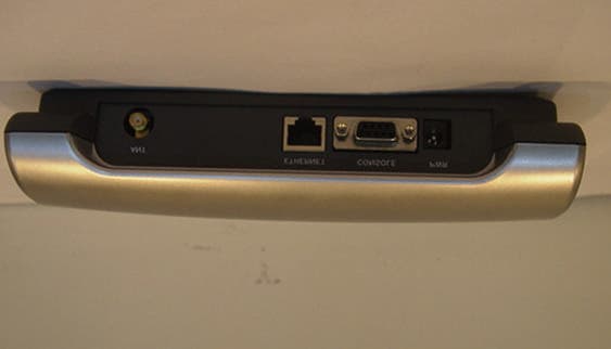
FFMLW1100AP
Nov 28, 2001WLAN Access Point
Equipment Class
DSS - Part 15 Spread Spectrum Transmitter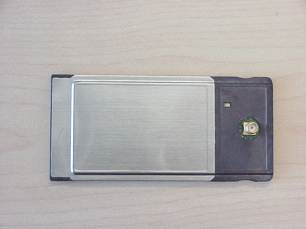
FFMLW1100N
Oct 25, 2001LP PCMCIA Card, model LW1100N
Equipment Class
DSS - Part 15 Spread Spectrum Transmitter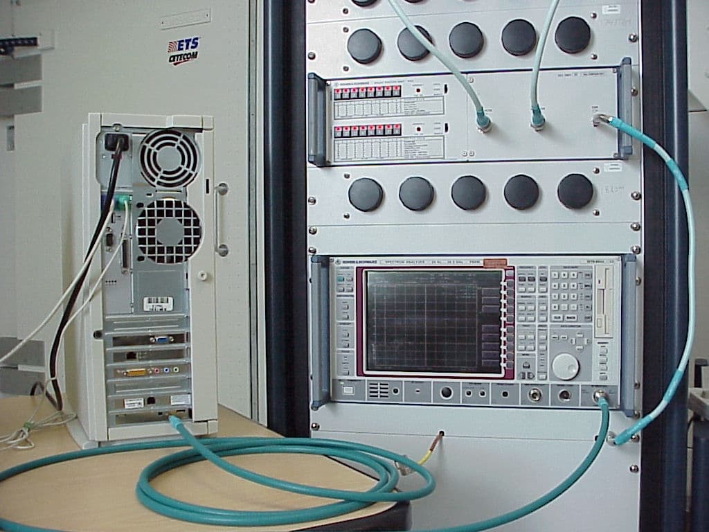
FFMLW1100P
Jul 10, 2001Wireless LAN PCI Card
Equipment Class
DSS - Part 15 Spread Spectrum Transmitter
FFMGT-8310C
Dec 07, 2000Cordless Phone
Equipment Class
DSS - Part 15 Spread Spectrum Transmitter