HFSWF1HNotebook PC
Quanta Computer Inc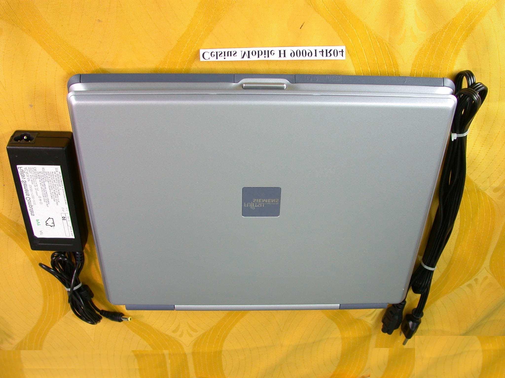
Click to zoom
Application Details
- Equipment Class
- DSS - Part 15 Spread Spectrum Transmitter
- Date of Grant
- Oct 08, 2001
- Application Purpose
- Original Equipment
- Date of Application
- Oct 08, 2001
- Equipment Note
- Notebook PC
- Frequency Range
- 2402.00000000 - 2480.00000000
- Company
- Quanta Computer Inc
- Country
- Taiwan
Documents & Files
Document Text
Text extracted from the exhibit documents filed with the FCC. Open a document above to read the original.
Users Manual
CELSIUS Mobile H EasyGuide Are there ... ... any technical problems or other questions you need clarified? Please contact: • your sales partner • your sales outlet You will find further information in the "Safety, Warranty and Ergonomics" booklet. The latest information on our products, tips, updates, etc., can be found on the Internet under: http://www.fujitsu-siemens.com Dieses Handbuch wurde auf Recycling-Papier gedruckt. This manual has been printed on recycled paper. Ce manuel est imprimé sur du papier recyclé. Este manual ha sido impreso sobre papel reciclado. Questo manuale è stato stampato su carta da riciclaggio. Denna handbok är tryckt på recyclingpapper. Dit handboek werd op recycling-papier gedrukt. Herausgegeben von/Published by Fujitsu Siemens Computers GmbH Bestell-Nr./Order No.: A26391-Kyyy-Z120-1-19 Printed in the Federal Republic of Germany AG 0601 06/01 CELSIUS Mobile H Operating Manual Introduction Important notes Preparing the notebook for use Working with your notebook Connecting external devices Settings in BIOS Setup Troubleshooting and tips Memory extension Technical data Index June 2001 edition DPMS and VESA are registered trademarks of Video Electronics Standards Association. Intel is a registered trademark, Pentium and Celeron are trademarks of Intel Corporation, USA. Microsoft, MS, MS-DOS, Windows, and Windows NT are registered trademarks of Microsoft Corporation. OS/2 and PS/2 are registered trademarks of International Business Machines, Inc. Zip is a trademark of Iomega Corporation. Macrovision is a trademark of Macrovision Corporation, USA. All other trademarks referenced are trademarks or registered trademarks of their respective owners, whose protected rights are acknowledged. Copyright Fujitsu Siemens Computers GmbH 2001 All rights, including rights of translation, reproduction by printing, copying or similar methods, in part or in whole, are reserved. Offenders will be liable for damages. All rights, including rights created by patent grant or registration of a utility model or design, are reserved. Delivery subject to availability. Right of technical modification reserved. A26391-Kyyy-Z120-1-7619 Contents A26391-Kyyy-Z120-1-76191 Introduction Your CELSIUS Mobile A is a versatile and ergonomic notebook. Innovative technology and ergonomic design make this notebook the ideal user-friendly and reliable travel companion. To simplify the initial start-up of your notebook, one or two operating systems are preinstalled on the hard disk (dual-installation). If two operating systems are preinstalled, you can select which of the two operating systems you want to install during initial start-up. The energy-saving processor and the energy-saving functions that can be configured allow you to make the most effective use of the battery capacity. Your notebook has 128 -1024 Mbyte of main memory installed, depending on the upgrade level. Data is stored on a hard disk drive. Your notebook is also equipped with a 3 1/2-inch disk drive. Depending on the model, your notebook is delivered with a CD-RW drive or a DVD-ROM drive. A PC card slot (CardBus or PCMCIA) enables the notebook to operate two type I or type II PC cards or one type III PC card. Depending on the variant, your notebook may be equipped with an internal mini-PCI board. Your notebook has connectors for external devices such as an external monitor, a printer, and a mouse. The ECP capable parallel port is designed for fast bidirectional data transfer. You can connect peripheral devices such as a scanner, loudspeakers, gamepads, keyboard, or mouse via the two USB ports. In addition, your notebook is equipped with a TV-Out connector to connect to a television. For mouse control, the notebook has a touchpad with touchpad buttons. An audio controller, two built in loudspeakers and a built in microphone provide your notebook with an audio capability. You can thus incorporate voice, noise effects and music into your notebook environment. You can also connect an external microphone and an external loudspeaker. The system settings of the notebook can be configured via the user-friendly BIOS Setup programme. Certain system settings (e.g. screen display, energy saving functions) can be modified via various key combinations while you are using the notebook. Your notebook has a number of security features to ensure that no unauthorised persons can access your data. For example, you can activate a screen saver with password protection. The security functions in the BIOS Setup also allow you to protect your data by means of passwords. This Operating Manual tells you how to put your notebook into operation and how to operate it in daily use. Additional information on your notebook is contained in the following documents: • in the manual „Safety and Ergonomics“ • in the manual "Getting Started" • in the documentation of the operating system • in the information files (e.g. *.TXT, *.DOC, *.WRI, *.HLP) 錯誤! 尚未定義樣式。錯誤! 尚未定義樣式。 2 Notational conventions The following symbols are used in this manual: ! Indicates information which is important for your health or for preventing physical damage. Failure to follow the instructions may lead to loss of data, invalidate your warranty, destroy the notebook, or endanger your life. i Indicates important information which is required to use the system properly. Ê Text which follows this symbol describes activities that must be performed in the order shown. This fontrepresents text output on the screen. This fontindicates programme names, commands, or menu items. "Quotation marks"indicate names of chapters, data carriers, and terms that are being emphasised. A26391-Kyyy-Z120-1-76193 Important notes Here you will find essential safety information regarding your notebook. In addition, the manufacturer's notes contain helpful information about your notebook. Safety ! Pay attention to the information provided in the manual "Safety and Warranty" and in the following security notes. Observe the sec…
Text truncated - open the document above for the full version.
Users Manual
The modem can be operated in the following countries: Multifrequency (MFC) dialling Belgium, Denmark, Germany, Finland, France, Greece, Great Britain, Holland, Ireland, Iceland, Italy, Luxembourg, Norway, Austria, Portugal, Sweden, Switzerland and Spain. Pulse dialling: Belgium, France, Holland and Italy. Also in: Poland, Slovenia, South Africa and Hungary. Connecting notebook modem to telephone connection 1 2 3 Ê Connect the modem cable supplied to the country-specific telephone adapter (1). Ê Connect the modem cable to the modem port of the notebook (2). Ê Connect the modem cable to your telephone wall socket (3). 錯誤! 尚未定義樣式。錯誤! 尚未定義樣式。 PC cards Two PC card slots enable the notebook to operate two type II PC cards or one type III PC card (CardBus or PCMCIA) . ! Consult the documentation supplied by the PC card's manufacturer and follow the instructions provided. Never use force when inserting or removing a PC card. Make sure that foreign objects do not fall into the PC card slot. Installing a PC card Ê Insert the PC card, contacts first, into the lower slot guide. The labelled side of the PC card must be facing upward. Ê Gently push the PC card into the slot until you feel it click into place. i Consult the documentation supplied with the PC card for information on how to install the necessary device drivers. For further information refer to the information files (e.g. *.TXT, *.DOC, *.WRI or *.HLP) provided on the PC card driver diskette or the information in the operating system manual. You can push the PC card slot eject buttons into the notebook casing. Press the eject buttons until they snap in. 錯誤! 尚未定義樣式。錯誤! 尚未定義樣式。 Removing a PC card 1 2 Ê Press the eject button (1). It will project further out of the notebook's case. If the eject buttons are pushed in flush with the notebook casing, they must first be snapped out. Press the eject buttons until they snap out. Ê Slide the PC card out of the notebook (2). SmartCards The SmartCard slot enables the notebook to operate one SmartCard. ! Consult the documentation supplied by the SmartCard's manufacturer and follow the instructions provided. Never use force when installing or removing a SmartCard. Make sure that foreign objects do not fall into the SmartCard slot. 錯誤! 尚未定義樣式。錯誤! 尚未定義樣式。 Inserting a SmartCard Ê Insert the SmartCard, contacts first, into the lower slot guide. The labelled side of the SmartCard must be facing upward. Ê Gently push the SmartCard into the slot until you feel it click into place. i Consult the documentation supplied with the SmartCard for information on how to install the necessary device drivers. For further information refer to the information files (e.g. *.TXT, *.DOC, *.WRI or *.HLP) provided on the SmartCard driver diskette or the information in the operating system manual. You can push the SmartCard slot eject buttons into the notebook casing. Press the eject buttons until they snap in. 錯誤! 尚未定義樣式。錯誤! 尚未定義樣式。 Pulling out a SmartCard 1 2 Ê Press the eject button (1). It will project further out of the notebook's case. If the eject buttons are pushed in flush with the notebook casing, they must first be snapped out. Press the eject buttons until they snap out. Ê Slide the SmartCard out of its location (2). 錯誤! 尚未定義樣式。錯誤! 尚未定義樣式。 Microphone and loudspeakers 1 2 a = built-in microphoneb = built-in loudspeakers Your notebook contains a built-in microphone (a) and two loudspeakers (b). If you attach an external microphone, the built-in microphone is disabled. The internal loudspeakers switch off when you attach headphones or external loudspeakers to the audio jack. 錯誤! 尚未定義樣式。錯誤! 尚未定義樣式。 Fingerprint ??? The notebook is equipped with a fingerprint reader. Instead of entering a user password, you can also log on to the system with a fingerprint. Before you can use the fingerprint reader, you must install the driver provided on the CD. Bluetooth Keyboard Product Specification ProductBluetooth Keyboard Radio Specification[1]Frequency range: 2.402 – 2.480 GHZ [2]RF output Power: Class 3 [3]Receiver Sensitivity: -70dBm at 0.1% BER [4]Cover distance: 3 meter (max) Electrical Characteristics [1]Power supply: Transmitter board at keyboard site will be powered by Li-ion 1100 mAh battery; receiver board at PC site is powered by 5Volt DC through USB connector [2]Power consumption: 80 mA max. (Transmitter board) [3]Visual indicator: LED indicators: Caps Lock, Num Lock, Scroll Lock, Battery status, Bluetooth connection status [4]Auto reconnecting: 錯誤! 尚未定義樣式。錯誤! 尚未定義樣式。 Automatically re-connect keyboard with notebook PC [5]Batter life: 24 hour (20,000 times key press) Intended use/purpose of the equipment Notebook with detachable K/B which can wireless communicate Notebook Type of modulationGFSK Channel spacing1Mhz Designation of emissionETSI 300 328 ETSI 300 826 Transmit RF power or power range -6 dBm ~ 0dBm Duty cycle625us Channel access protocol TDMA Duplex directionDuplex Antenna TypeMicro Strip ANT Peak Gain > 3dBi, <-5dBi Vswr<= 2 Return loss <= -10 dBm Reference standard or other specification Bluetooth spec. V1.1 錯誤! 尚未定義樣式。錯誤! 尚未定義樣式。 Property and data protection Your notebook enables you to protect your system and personal data in a number of ways against unauthorised access. By combining these options, you can achieve maximum protection for your system. Security panel a a = Security panel The security panel enables you to protect your notebook from unauthorised use with a hardware password. When a Security Panel password is activated, the notebook will not start without the correct insertion of a password. The password is entered before the BIOS is read out and the hardware activated. The password is requested from all suspend and resume modes. As a result, a security level is also provided with the energy-saving mode activated. The Security Lock function can be used when the notebook is started from the Resume mode, when switched off and from the Save-to-Disk mode. Password protection of Save-to-RAM Mode is also…
Text truncated - open the document above for the full version.
External Photos
Page 1 ANNEX PHOTOGRAPHS OF EUT Page 2
External Photos
Page 3 Page 4
External Photos
Page 5 Page 6 Page 7
ID Label/Location Info
Label Location
ID Label/Location Info
D D 1 2 3 4 5 6 7 ABCE 7 6 5 4 3 2 1 ECBA LTR NAME MODEL MATERIAL FINISH DATE SCALE UNIT MM DWG. NO. APPROVED DESIGNED DRAWN REV 3B 3A 3B 3C TOL. + - 1 PLC2 PLCANGLE 7F, 116 HOU KANG ST. SHIN LIN, TAIPEI, TAIWAN, R.O.C. ITEMDESCRIPTION REVISIONS DESCRIPTION DATEAPP THE 3RD PROJECTION PART NO. Quanta Computer Inc. 2 1 3 FIRST RELEASE Rita HCWF1002 1/1 HCWF1002018 90.09.21 90.08.08 Wf1 RATING LABEL(H) SEE NOTES Rita FREE SEE NOTES , 0.1 5 2 . 6 83.75 R4.3X4 CELSIUS Mobile CELSIUS Mobile H P/N : S26391-K115-V1 FUJITSU SIEMENS COMPUTERS MADE IN TAIWAN Model No : WF1H Contains : Lithium Battery, Must be recycled or disposed of Properly. The Windows logo is a registered trademark of Microsoft Corporation. DC 19V 4.20A EPA POLLUTION PREVENTER TH10 CM ITE S/N : REV. : CHANGE TEXT 90.09.21 Rita 3B FCC ID : HFSWF1H This device complies with Part 15 of the FCC Rules. Operation is subject to the following two conditions: (1) This device may not cause harmful interference, and (2) this device must accept any interference received, including interference that may cause undesired operation.
Internal Photos
Page 8 Page 9 Page 10
Internal Photos
Page 11 Page 12
Internal Photos
Page 13 Page 14
Internal Photos
Page 15 Page 16
Internal Photos
Page 17 Page 18
Internal Photos
Page 19 Page 20
Operational Description
FCC ID: HFSWF1H ADT No.900914R04 Operational Description The EUT (Notebook PC) includes two individual parts. One is the Keyboard which cand be removed from the EUT, the other is Notebook. The Keyboard is powered by 3VDC battery and Notebook PC power is 5VDC. This device is a Frequency Hopping device with 79 hopping frequencies. The declared output power is only +4dBm. The bluetooth transceiver is installed on both notebook and keyboard.
RF Exposure Info
5 5 4 4 3 3 2 2 1 1 DD CC BB AA CC&C Technologies, Inc. FOR ESD FOR ESD 70-140501-0D 0 SC-405 Keyboard End / Keyboard Encoder B 24Wednesday, August 22, 2001 Title SizeDocument NumberRev Date:Sheetof Scroll_Lock_LED KBCN_11 TPCLK KBCN_24 KBCN_13 KBCN_17 KBCN_20 KBCN_14 TPDATA BT_LED# KBCN_9 KBCN_15 Num_Lock_LED KBCN_16 KBCN_21 Caps_Lock_LED KBCN_12 KBCLK KBDATAKBCN_8 KBCN_18 KBCN_10 KBCN_23 BT_ACTIVE# KBCN_22 KBCLK KBDATA TPCLK TPDATA KBCN_19 KBCN_2 KBCN_5 KBCN_7 KBCN_6 KBCN_4 KBCN_3 KBCN_1 KBCN_1 KBCN_2 KBCN_3 KBCN_4 KBCN_6 KBCN_5 KBCN_7 KBCN_9 KBCN_11 KBCN_10 KBCN_12 KBCN_8 KBCN_13 KBCN_22 KBCN_15 KBCN_23 KBCN_17 KBCN_19 KBCN_16 KBCN_24 KBCN_21 KBCN_20 KBCN_18 KBCN_14 BT_LED# TPDCLK TPDDATA BT_ACTIVE# Caps_Lock_LED Scroll_Lock_LED Num_Lock_LED VMUX VCC3 VCC3 C10320PF C9620PF C10620PF C8520PF C9720PF C10020PF C88 0.1UF C8220PF Y41 4MHz C43 20PF C9820PF C44 20PF C9920PF C10820PF C42 0.1UF C9520PF C8920PF C8420PF C8320PF U41 EM78P451 1234567891011 12 13 14 15 16 17 18 19 20 21 22 232425262728293031 34 3332 35 36 37 38 39 40 41 42 43 44 P9.0P9.1P9.2P9.3P9.4P9.5P5.0P5.1P5.2P5.3P5.4 P5.5 P5.6 P5.7 P8.0 P8.1 N.C P8.2 P8.3 P8.4 P8.5 P8.6 P8.7P6.0P6.1P6.2P6.3P6.4P6.5P6.6P6.7 P7.0 P7.1P7.2 N.C N.C N.C VDD XIN XOUT VSS # INT DATA CLK C10920PF JP42 HEADER 24 1 2 3 4 5 6 7 8 9 10 11 12 13 14 15 16 17 18 19 20 21 22 23 24 C10420PF C8720PF C10520PF C11220PF C10120PF JP41 HEADER 10 1 2 3 4 5 6 7 8 9 10 C9020PF RN41 10KX4/3216 1 2 3 45 6 7 8 C11120PF C41 4.7UF C9120PF C10220PF C9320PF C9420PF C8620PF C10720PF C11020PF C9220PF C8120PF KBCLK3 KBDATA3 BAT_LED#3,4 BT_ACTIVE#3 TPCLK3 TPDATA3 5 5 4 4 3 3 2 2 1 1 DD CC BB AA CC&C Technologies, Inc. 70-140501-0D 0 SC-405 Keyboard End / Keyboard Encoder B 34Wednesday, August 22, 2001 Title SizeDocument NumberRev Date:Sheetof RXD CTS_BT +2V8_RADIO RTS_BT GND_POWER SPI_CSB SPI_MISO ISP# TXD BT_RST SPI_MOSI SPI_CLK EA# CTS_51 RXD TXD TEST RTS_51 TEST 9346_DO 9346_DI 9346_CLK 9346_CLK 9346_DI 9346_DO 9346_CS 9346_CS BT_RST CTS_51RTS_BT CTS_BTRTS_51 ISP# ISP# RST VCC3 VCC3 VNB1 VCC3 VCC3 VCC3 VCC3 VCC5 VCC3 C48 10UF/10V Q43 2N7002 R64 0_OP C113 20PF R91 0_OP R50 10K U53 93C46 1 2 3 45 8 6 7 CS CLK DI DOGND VCC NC1 NC2 C47 4.7UF R8810K R950_OP U46 BLUETOOTH MODULE 0 dBm A1 A2 A3 A4 A5 A6 B1 B2 B3 B4 B5 B6 C1 C2 C3 C4 C5 C6 R1 R2 R3 R4 R5 R6 T1 T2 T3 T4 T5 T6 PCM_A PCM_B PCM_SYNC PCM_CLK RXD RTS D+ D- GND WAKE_UP TXD CTS DETACH ON I2C_CLK VCC_IO ON# VCC GND GND RESET# NC NC NC GND ANT GND NC NC I2C_DATA VREG PIO7 PIO6 PIO4 TEST_A TEST_B SPI_MISO SPI_MOSI SPI_CLK SPI_CSB GND_POWER +2V8_RADIO R630 Y42 22.1184MHZ C45 1UF U43 W78LE58 1 2 3 4 5 6 7 8 9 10 11 1213141516171819202122 23 24 25 26 27 28 29 30 31 32 33 3435363738394041424344 P1.5 P1.6 P1.7 RST RXD/P3.0 INT2#/P4.3 TXD/P3.1 INT0#/P3.2 INT1#/P3.3 T0/P3.4 T1/P3.5 WR#/P3.6RD#/P3.7XTAL2XTAL1VSSP4.0A8/P2.0A9/P2.1A10/P2.2A11/P2.3A12/P2.4 A13/P2.5 A14/P2.6 A15/P2.7 PSEN# ALE P4.1 EA# AD7/P0.7 AD6/P0.6 AD5/P0.5 AD4/P0.4 AD3/P0.3AD2/P0.2AD1/P0.1AD0/P0.0 VDD INT3#/P4.2 T2/P1.0 T2EX/P1.1 P1.2P1.3P1.4 C51 20P R49 10K C49 20P SW1 SW PUSHBUTTON R79 10K R940 Q41 2N7002 R5210K JP46 1.27-12P 1 2 3 4 5 6 7 8 9 10 11 12 JP44 HRS-CL331 1 2 3 GND GND OUT C53 1UF R89 0 R90 0_OP TX_51 BT_ACTIVE#2 KBCLK2 TPCLK2 TPDATA2 KBDATA2 RESET# BATLO_FLASH4 BAT_LED#2,4 CHRG#2,4 RESET# RX_51 BATLOW# 4 BATLO_FLASH 2 5 5 4 4 3 3 2 2 1 1 DD CC BB AA CC&C Technologies, Inc. 2 4 OVER 4.6 V RESET=>HIGH 3 3 1 Charger shutdown 57'C - 62'C ACTIVE IF A3 BATTREY IS NOT AVAILABLE 1 UNDER 4.6 V RESET=>LOW SOT23 SOT23-5 2 5 3.8V 3.0V BATLOW#: 3.26V Original is VMUX, chage to VNB1 at R.D Original is VMUX, chage to VCC3 at R.D 70-140501-0D 0 SC-405 Keyboard End / Keyboard Encoder B 44Wednesday, August 22, 2001 Title SizeDocument NumberRev Date:Sheetof SHDN# REF1.225V BATTEMP VNB1 REF1.225V REF1.225V VNB2 SHDN# SHDN# SHDN# VMUX VNB VBAT VCC5 VCC5 VNB1 VNB1 VCC3 VNB1 VBAT V3_ALWAYSVBAT VBAT VCC3 VNB1 VNB1 VNB1 VNB VCC3 V3_ALWAYS VCC3 VCC5 V5_ALWAYS VCC3 VNB1 C63 1UF R84 2K-1% 1 2 Q45 SI2301DS D G S R856.9K-1% 12 JP43 HEADER 2 1 2 C54 10UF/10V_OP R68 10K 1 2 R69 20K 1 2 R81 100K 1 2 R67 100K 1 2 Q46 SI3457 312 456 + C62 10U/10V 1 2 C80 0.1UF C58 0.1UF R83 3K-1% 1 2 R71 19.6K-1% 1 2 C57 4.7UF Q47 DTC114EKA 1 3 2 C59 0.1UF_OP R65 6.9K-1%_OP 1 2 D41 EC10QS04 21 D42 LM4041-1.225V E B C R66 3.6K-1% 1 2 + - U51A LM393 3 2 1 8 4 R80 0 1 2 U50 LTC1732-4 1 2 3 4 5 10 9 8 7 6 BAT SEL CHRG TIMER GND ACPR SENSE VCC DRV PROG R70 0.2 1 2 + C55 47U/6.3V_OP 1 2 C118 0.1UF C56 0.01UF L41 22uH_OP 1 2 C115 20PF JP45 HEADER 4 1 2 3 4 U48 MAX1674_OP 1 2 3 45 6 7 8 FB LBI LBO REFSHDN- GND LX OUT R73 10K 1 2 R87 10K 1 2 R82 3K-1% 1 2 C117 4.7UF R9910K 12 Q50 SI2301DS D G S C60 0.1UF_OP R42 0 12 Q49 DTC114EKA 1 3 2 R75 3K-1% 1 2 R96 100K 12 R43 0_OP 1 2 JP47 HEADER 2 12 R97 0 12 Q48 DTC114EKA 1 3 2 R74 3.6K-1% 1 2 + - U52B LM393 5 6 7 C64 0.1UF R92 51K 1 2 + - U52A LM393 3 2 1 8 4 + - U51B LM393 5 6 7 C116 0.1UF U42 MAX809L 12 3 GNDRESET VCC R760 12 R770_OP 12 R862K-1% 12 Q44 SI2301DS D G S C52 0.1UF Q51 SI2301DS D G S Q52 2N7002 C61 4.7UF R98 100 1 2 U45 MIC5219-3.3BM5 5 4 1 3 2 OUT BP IN SHDN# GND CHRG#2,3 BATLOW#3
Test Report
FCC ID: HFSWF1H Report No.: RF900914R04 1 Issued: October 2, 2001 FCC TEST REPORT REPORT NO.: RF900914R04 MODEL NO.: Celsius Mobile H RECEIVED: Sept. 14, 2001 TESTED: Sept. 11 ~ Sept. 27, 2001 APPLICANT: QUANTA COMPUTER INC. ADDRESS: 7F, 116 Hou Kang St., Shih Lin, Taipei, Taiwan, R.O.C. ISSUED BY: Advance Data Technology Corporation LAB LOCATION: 47 14th Lin, Chiapau Tsun, Linko, Taipei, Taiwan, R.O.C. This test report consists of 87 pages in total. It may be duplicated completely for legal use with the approval of the applicant. It should not be reproduced except in full, without the written approval of our laboratory. The client should not use it to claim product endorsement by CNLA, NVLAP or any government agencies. The test results in the report only apply to the tested sample. 0528 Lab Code: 200102-0 FCC ID: HFSWF1H Report No.: RF900914R04 2 Issued: October 2, 2001 Table of Contents 1CERTIFICATION ........................................................................................................ 4 2SUMMARY OF TEST RESULTS ................................................................................ 5 3GENERAL INFORMATION......................................................................................... 6 3.1GENERAL DESCRIPTION OF EUT ........................................................................... 6 3.2DESCRIPTION OF TEST MODES ............................................................................. 7 3.3GENERAL DESCRIPTION OF APPLIED STANDARDS ............................................. 7 3.4DESCRIPTION OF SUPPORT UNITS........................................................................ 8 4TEST PROCEDURES AND RESULTS....................................................................... 9 4.1CONDUCTED EMISSION MEASUREMENT .............................................................. 9 4.1.1LIMITS OF CONDUCTED EMISSION MEASUREMENT ...................................... 9 4.1.2TEST INSTRUMENTS .......................................................................................... 9 4.1.3TEST PROCEDURES ........................................................................................ 10 4.1.4TEST SETUP ..................................................................................................... 10 4.1.5TEST RESULTS(A)............................................................................................. 11 4.1.6Test Results(B) ................................................................................................... 12 4.2NUMBER OF HOPPING FREQUENCY USED......................................................... 18 4.2.1LIMIT OF HOPPING FREQUENCY USED ......................................................... 18 4.2.2TEST INSTRUMENTS ........................................................................................ 18 4.2.3TEST PROCEDURES ........................................................................................ 19 4.2.4TEST SETUP ..................................................................................................... 19 4.2.5TEST RESULTS (A)............................................................................................ 19 4.2.6TEST RESULTS (B)............................................................................................ 22 4.3DWELL TIME ON EACH CHANNEL......................................................................... 25 4.3.1LIMIT OF DWELL TIME USED ........................................................................... 25 4.3.2TEST INSTRUMENTS ........................................................................................ 25 4.3.3TEST PROCEDURES ........................................................................................ 26 4.3.4TEST SETUP ..................................................................................................... 26 4.3.5TEST RESULTS (A)............................................................................................ 27 4.3.6TEST RESULTS (B)............................................................................................ 31 4.4CHANNEL BANDWIDTH.......................................................................................... 35 4.4.1LIMITS OF CHANNEL BANDWIDTH.................................................................. 35 4.4.2TEST INSTRUMENTS ........................................................................................ 35 4.4.3TEST PROCEDURE........................................................................................... 36 4.4.4TEST SETUP ..................................................................................................... 36 4.4.5EUT OPERATING CONDITION .......................................................................... 36 4.4.6TEST RESULTS (A)............................................................................................ 37 FCC ID: HFSWF1H Report No.: RF900914R04 3 Issued: October 2, 2001 4.4.7TEST RESULTS (B)............................................................................................ 41 4.5HOPPING CHANNEL SEPARATION........................................................................ 45 4.5.1LIMIT OF HOPPING CHANNEL SEPARATION .................................................. 45 4.5.2TEST INSTRUMENTS ........................................................................................ 45 4.5.3TEST PROCEDURES ........................................................................................ 46 4.5.4TEST SETUP ..................................................................................................... 46 4.5.5TEST RESULTS (A)............................................................................................ 47 4.5.6TEST RESULTS (B)............................................................................................ 51 4.6MAXIMUM PEAK OUTPUT POWER........................................................................ 55 4.6.1LIMITS OF MAXIMUM PEAK OUTP…
Text truncated - open the document above for the full version.
Test Report
FCC ID: HFSWF1H The BlueTooth module used in this product is from CSR. As discussed between Mr. J. Dichoso (FCC) and Mr. C. Neal (CSR), all BC01 based modules are deemed to have identical processing gains, and as such, the test report for product FCC ID: O2Z-BT2 can be submitted as evidence for the Processing Gain requirements. Since the BlueTooth technique used in this product is from the same chip, BC01. So, the processing gain test result is attached. Page 1 of 11 Properties/Title v2 15 February 2001 MEMORANDUM – PROCESSING GAIN REPORT FOR INTEL(R) PERSONAL WIRELESS MODULE Subject: Results of Processing Gain Tests for FCC Qualification 1 INTRODUCTION This memo presents the results of the Processing Gain (PG) tests carried out for FCC qualification of the Intel(R) Personal Wireless Module chip. The FCC states that the PG from a hybrid Bluetooth receiver must be greater than 17 dB when measured in accordance with the Continuous Wave (CW) jamming margin method. Testing of the Intel(R) Personal Wireless Module “B” Bluetooth chip has found the PG due to the DS section to be approximately 5 dB and the PG due to the FH part to be approximately 15 dB. It is therefore concluded that the Intel(R) Personal Wireless Module Bluetooth Chip complies with the FCC PG requirements for radio communication systems. The rest of this paper outlines the PG measurement technique and discusses the test results. Appendix A contains a list of test equipment and Appendix B contains a printout of the measurement results. 2 METHOD 2.1 PG Definition The Processing Gain from a frequency hopping communication system is derived from two parts, the FH section and the DS section. The PG due to FH is given by a simple equation and is constant. However measurement of the PG due to DS is a little more complex. One technique is to use the CW jamming margin method. This method measures PG due to DS using the following algorithm: A CW signal generator is stepped in 50kHz increments across the passband of the system, recording at each point the generator level required to produce the 0.1% Packet Error Rate (PER). This is the jammer level. This level is then referenced to the output power of the intended Bluetooth signal and the Jammer to Signal Ratio JSR is thus calculated. The worst 4 JSR measurements are discarded and the worst remaining JSR is used to calculate the PG due to DS as follows: sysp LJSRSNRG++= min Page 2 of 11 Properties/Title v2 15 February 2001 where G p = the processing gain of the system, SNR = the signal to noise ratio required for 0.1% BER, JSR min = minimum J/S ratio and L sys = system losses. 2.2 PG Measurement Technique Figure 1 provides an overview of the PG measurement technique. The measurement is performed in two parts, measurement of the system SNR and measurement of JSR min . Figure 1: PG Measurement Technique The system SNR is calculated using the following algorithm. Generate Bluetooth PRBS-9 packets using a Bluetooth chip emulator (1) and a Vector Signal Generator (2). Combine this signal with white noise of a constant level, which is generated using a noise source (4) and a CW Signal Generator (3). Then vary the level of the Bluetooth signal until the BER measured by the Bluetooth chip (7) is 0.1%. The resulting SNR is the signal level divided by the Noise level. Page 3 of 11 Properties/Title v2 15 February 2001 The JSR for a given jamming frequency is calculated using the following algorithm. Generate Bluetooth PRBS-9 packets using the Bluetooth chip emulator (1) and the Vector Signal Generator (2). Combine this signal with a constant CW tone at the jamming frequency using a CW Signal Generator (5) and a combiner (6). Then vary the level of the Bluetooth signal until the PER measured by the Casira Bluetooth Module (7) is 0.1%. The resulting JSR is the signal level divided by the jamming level. 3 RESULTS 3.1 Overview The measurements found that the PG due to DS caused by the access code in page and inquiry mode is found to be approximately 5dB when the access code is a relatively random mixture of 1's and 0's. A random access code causes the most Inter Symbol Interference (ISI) and hence the worst PG for a hybrid system. Therefore only the results for this access code are used in the PG calculation. The PG due to FH is given as PG FH = 10 log 10 (number of frequency hops) The number of hops in a Bluetooth system is 32, therefore the PG due to FH is approximately 15 dB. When this is added to the PG due to DS, the total PG for the Bluetooth chip is approximately 20 dB, above the minimum PG requirement for FCC qualification. 3.2 Detailed Results Test Date: 17/11/00 Sample Time: 30 seconds Access Code: c6967e Signal Frequency: 2.432GHz Receiver Sensitivity: -88.7 dBm Jammer Signal Level: -85.7 dBm Measured SNR: 18.8dB System Losses: 2dB To calculate processing gain, ignore the worst 20% of data points and then apply the following formula: Page 4 of 11 Properties/Title v2 15 February 2001 sysp LJSRSNRG++= min Where G p = Processing Gain of the module SNR = signal to noise ratio of the module JS min = minimum J/S ratio after the worst 20% of J/S samples have been discarded L sys = System losse…
Text truncated - open the document above for the full version.
Contact Information
Applicant
Joyce Kuo
Technical Contact
Advance Data Technology CorporationAlan Lane
[email protected]+886 3 327 0910
13-1, Lane 19, WenShan 3rd St. · Taoyuan · Taiwan
Test Firm
Bureau Veritas CPS (H.K.) Ltd. Taoyuan BranchRichard Chen
Technical Specifications
| # | Rule Parts | Frequency Range | Power Output |
|---|---|---|---|
| 1 | 15C | 2.40 GHz - 2.48 GHz | 3.80 mW |
Other Applications from Quanta Computer Inc
HFS-C306
Sep 03, 2026Mini
Equipment Class
DTS - Digital Transmission SystemHFS-QV28NRW
Jul 15, 2026Telematics Module
Equipment Class
PCB - PCS Licensed TransmitterHFSCIP
Jun 15, 2026QOCA ecg1202
Equipment Class
DTS - Digital Transmission System
HFS-QV28NUS
Apr 16, 2026Telematics Module
Equipment Class
PCB - PCS Licensed TransmitterHFS-C407
Jul 21, 2024Clover Flex Pocket
Equipment Class
NII - Unlicensed National Information Infrastructure TX