HLEMS852PWWireless 2D Imager Scanner
Unitech Electronics Co., Ltd.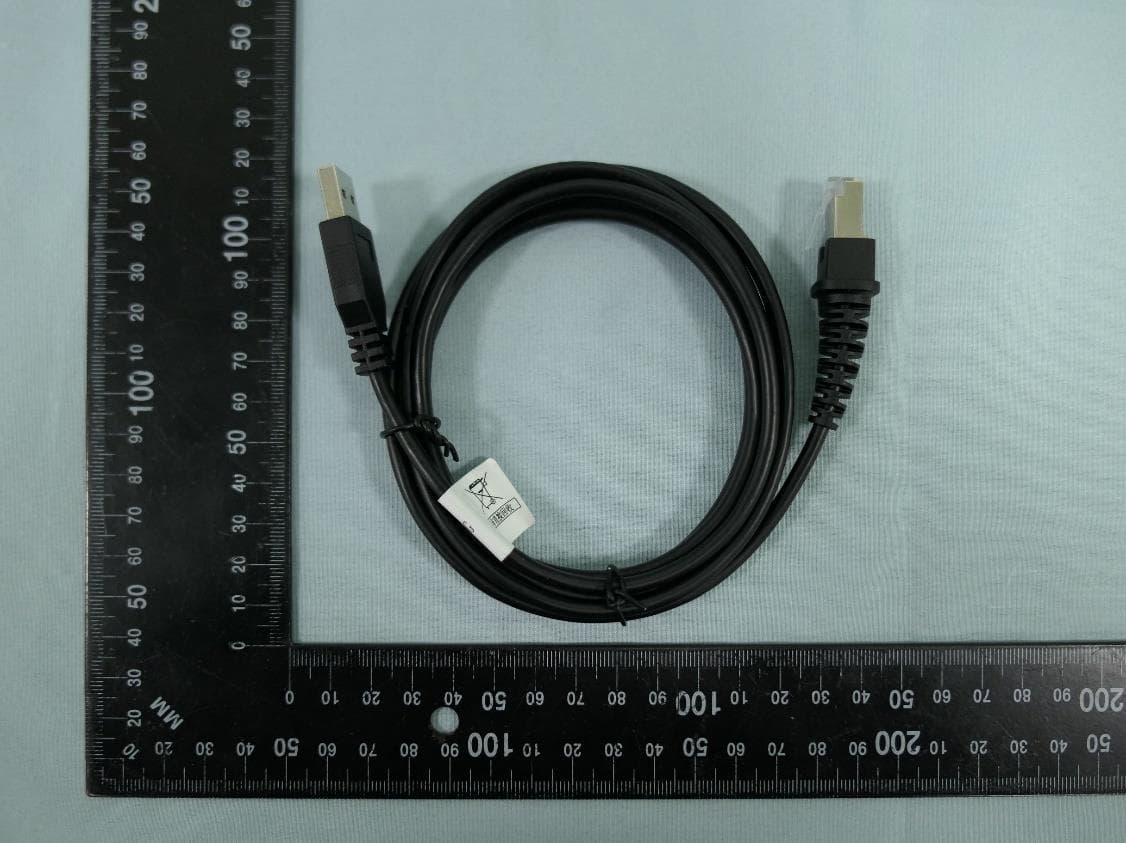
Click to zoom
Application Details
- Equipment Class
- DTS - Digital Transmission System
- Date of Grant
- Dec 22, 2022
- Application Purpose
- Original Equipment
- Date of Application
- Dec 20, 2022
- Equipment Note
- Wireless 2D Imager Scanner
- Frequency Range
- 2410.00000000 - 2470.00000000
- Country
- Taiwan
Documents & Files
Document Text
Text extracted from the exhibit documents filed with the FCC. Open a document above to read the original.
Users Manual
2D Imager Scanner - MS852P - User's Manual Version 1.0 Revision History Date Change Description Version 20221011 First Version 1.0 i © 2022 Unitech Electronics Co., Ltd. All rights reserved. Unitech is a registered trademark of Unitech Electronics Co., Ltd. All product and company names are trademarks, service marks, or registered trademarks of their respective owners About This Manual Preface Thank you for purchasing the Unitech product. This manual explains how to install, operate and maintain our product. No part of this publication may be reproduced or used in any form, or by any electrical or mechanical means, such as photocopying, recording, or information storage and retrieval systems, without permission in writing from the manufacturer. The material in this manual is subject to change without notice. Regulatory Compliance Statements FCC Warning Statement This device has been tested and found to comply with the limits for a Class B digital device, pursuant to part 15 of the FCC rules. These limits are designed to provide reasonable protection against harmful interference in a residential installation. This equipment generates, uses and can radiate radio frequency energy and, if not installed and used in accordance with the instructions, may cause harmful interference with radio communications. However, there is no guarantee that interference will not occur in a particular installation. If this equipment does cause harmful interference with radio or television reception, which can be determined by turning the equipment off and on, the user is encouraged to try to correct the interference by one or more of the following measures: –Reorient or relocate the receiving antenna. –Increase the separation between the equipment and receiver. –Connect the equipment into an outlet on a circuit different from that to ii © 2022 Unitech Electronics Co., Ltd. All rights reserved. Unitech is a registered trademark of Unitech Electronics Co., Ltd. All product and company names are trademarks, service marks, or registered trademarks of their respective owners which the receiver is connected. –Consult the dealer or an experienced radio/TV technician for help. 1.This transmitter must not be co-located or operating in conjunction with any other antenna or transmitter. 2.This device complies with FCC RF radiation exposure limits set forth for an uncontrolled environment. To maintain compliance with FCC RF exposure requirements, avoid direct contact to the transmitting antenna during transmitting. 3.Any changes or modifications (including the antennas) made to this device that are not expressly approved by the manufacturer may void the user’s authority to operate the equipment. FCC Label Statement This device complies with part 15 of the FCC rules. Operation is subject to the following two conditions: 1.This device may not cause harmful interference. 2.This device must accept any interference received, including interference that may cause undesired operation. RF Radiation Exposure Statement This device contains transmitters and receivers which emit Radio Frequency (RF) energy. The device is designed to comply with the limits for exposure to RF energy set by the Federal Communications Commission (FCC) of the United States. European Conformity Statement Unitech Electronics co., Ltd herewith declares that the Unitech product is in compliance with the essential requirements and all other provisions of the RED 2014/53/EU directive. The declaration of conformity is available for download at : https://portal.Unitech.eu/public/Safetyregulatorystatement iii © 2022 Unitech Electronics Co., Ltd. All rights reserved. Unitech is a registered trademark of Unitech Electronics Co., Ltd. All product and company names are trademarks, service marks, or registered trademarks of their respective owners CE RF Exposure Compliance For body-worn operation, this device has been tested and meets the ICNIRP guidelines and the European Standard EN 62209-2, for use with dedicated accessories, SAR is measured with this device at a separation of 0.5 cm to the body, while transmitting at the highest certified output power level in all frequency bands of this device. Use of other accessories which contain metals may not ensure compliance with ICNIRP exposure guidelines. CE Mark Warning iv © 2022 Unitech Electronics Co., Ltd. All rights reserved. Unitech is a registered trademark of Unitech Electronics Co., Ltd. All product and company names are trademarks, service marks, or registered trademarks of their respective owners RoHS Statement This device conforms to RoHS (Restriction Of Hazardous Substances) European Union regulations that set maximum concentration limits on hazardous materials used in electrical and electronic equipment. Waste electrical and electronic equipment (WEEE) Unitech has set up a policy and process to meet the 2012/19/EU concerning electronic waste disposal. For more detailed information of the electronic waste disposal of the products you have purchased from Unitech directly or via Unitech’s resellers, you shall either contact your local supplier or visit us at : https://portal.Unitech.eu/public/WEEE v © 2022 Unitech Electronics Co., Ltd. All rights reserved. Unitech is a registered trademark of Unitech Electronics Co., Ltd. All product and company names are trademarks, service marks, or registered trademarks of their respective owners Taiwan NCC Warning Statement NCC 警語 取得審驗證明之低功率射頻器材,非經核准,公司、商號或使用者均不得擅自變 更頻率、加大功率或變更原設計之特性及功能。低功率射頻器材之使用不得影響 飛航安全及干擾合法通信;經發現有干擾現象時,應立即停用,並改善至無干擾 時方得繼續使用。前述合法通信,指依電信管理法規定作業之無線電通信。低功 率射頻器材須忍受合法通信或工業、科學及醫療用電波輻射性電機設備之干擾。 注意事項: 1.使用過度恐傷害視力。 2.使用30分鐘請休息10分鐘;2歲以下幼兒不看螢幕,2歲以上每天看螢幕不要超過 1小時。 3.減少電磁波影響,請妥適使用。 vi © 2022 Unitech Electronics Co., Ltd. All rights reserved. Unitech is a registered trademark of Unitech Electronics Co., Ltd. All product and company names are trademarks, service marks, or registered trademarks of their respective owners Laser Information The Unitech product is certified…
Text truncated - open the document above for the full version.
External Photos
Report No.: 2210TW2602-U1 Product: Wireless 2D Imager Scanner Brand Name: unitech Model Number: MS852P 1 of 14 External Photograph (1) EUT Photo (2) EUT Photo Report No.: 2210TW2602-U1 2 of 14 (3) EUT Photo (4) EUT Photo Report No.: 2210TW2602-U1 3 of 14 (5) EUT Photo (6) EUT Photo Report No.: 2210TW2602-U1 4 of 14 (7) EUT Photo (8) Dongle Photo Report No.: 2210TW2602-U1 5 of 14 (9) Dongle Photo (10) Dongle Photo Report No.: 2210TW2602-U1 6 of 14 (11) Dongle Photo (12) Dongle Photo Report No.: 2210TW2602-U1 7 of 14 (13) Dongle Photo (14) Docking Photo Report No.: 2210TW2602-U1 8 of 14 (15) Docking Photo (16) Docking Photo Report No.: 2210TW2602-U1 9 of 14 (17) Docking Photo (18) Docking Photo Report No.: 2210TW2602-U1 10 of 14 (19) Docking Photo (20) Docking Photo Report No.: 2210TW2602-U1 11 of 14 (21) USB Adapter Photo (22) USB Adapter Photo Report No.: 2210TW2602-U1 12 of 14 (23) USB Adapter Photo (24) USB Adapter Photo Report No.: 2210TW2602-U1 13 of 14 (25) USB Adapter Photo (26) USB Adapter Photo Report No.: 2210TW2602-U1 14 of 14 (27) USB Adapter Photo (28) USB to LAN Cable Photo
ID Label/Location Info
Label Label location
Internal Photos
Report No.: 2210TW2602-U1~U2 Product: Wireless 2D Imager Scanner Brand Name: unitech Model Number: MS852P 1 of 9 Internal Photograph (1) EUT Photo (2) EUT Photo Report No.: 2210TW2602-U1~U2 2 of 9 (3) EUT Photo (4) EUT Photo Report No.: 2210TW2602-U1~U2 3 of 9 (5) EUT Photo (6) EUT Photo Report No.: 2210TW2602-U1~U2 4 of 9 (7) EUT Photo (8) EUT Photo Report No.: 2210TW2602-U1~U2 5 of 9 (9) EUT Photo (10) EUT Photo Report No.: 2210TW2602-U1~U2 6 of 9 (11) EUT Photo (12) EUT Photo Report No.: 2210TW2602-U1~U2 7 of 9 (13) EUT Photo (14) EUT Photo Report No.: 2210TW2602-U1~U2 8 of 9 (15) EUT Photo (16) EUT Photo Report No.: 2210TW2602-U1~U2 9 of 9 (17) EUT Photo (18) EUT Photo
RF Exposure Info
MRT Technology (Taiwan) Co., Ltd Report No.: 2210TW2602-U2 Phone: +886-3-3288388 Report Version: 1.0 Fax: +886-3-3288918 Issue Date: 2022-12-14 Web: www.mrt-cert.com FCC ID: HLEMS852PW Page Number: 1 of 5 RF Exposure Evaluation Declaration FCC ID : HLEMS852PW Applicant : Unitech Electronics Co., Ltd. Application Type : Certification Product : Wireless 2D Imager Scanner Model No. : MS852P Brand Name : unitech FCC Rule Part(s) : Part 2.1093 (Portable) Test Procedure(s) : KDB 447498 D01v06 Received Date : October 03, 2022 Test Date : December 08, 2022 Reviewed By : ( Paddy Chen ) Approved By : ( Chenz Ker) The test results relate only to the samples tested. This equipment has been shown to be capable of compliance with the applicable technical standards as indicated in the measurement report. Test results reported herein relate only to the item(s) tested. The test report shall not be reproduced except in full without the written approval of MRT Technology (Taiwan) Co., Ltd. Report No.: 2210TW2602-U2 FCC ID: HLEMS852PW Page Number: 2 of 5 Revision History Report No. Version Description Issue Date Note 2210TW2602-U2 1.0 Original Report 2022-12-14 Report No.: 2210TW2602-U2 FCC ID: HLEMS852PW Page Number: 3 of 5 1. PRODUCT INFORMATION 1.1. Equipment Description 1.2. Antenna Description No. Manufacturer Part No. Antenna Type Peak Gain 1 ACX AT8010-E2R9HAA Chip 2.5dBi Product Name Wireless 2D Imager Scanner Model No. MS852P Brand Name unitech Operating Frequency 2.4G Modulation Type GFSK Report No.: 2210TW2602-U2 FCC ID: HLEMS852PW Page Number: 4 of 5 2. MAXIMUM PERMISSIBLE EXPOSURE (MPE) 2.1. FCC Limits According to FCC KDB 447498 Section 4.3 - General SAR test exclusion guidance For 100 MHz to 6 GHz and test separation distances ≤ 50 mm, the 1-g and 10-g SAR test exclusion thresholds are determined by the following: [(max. power of channel, including tune-up tolerance, mW) / (min. test separation distance, mm)] · [√f(GHz)] ≤ 3.0 for 1-g SAR, and ≤ 7.5 for 10-g extremity SAR, where 1. f(GHz) is the RF channel transmit frequency in GHz 2. Power and distance are rounded to the nearest mW and mm before calculation 3. The result is rounded to one decimal place for comparison 4.The values 3.0 and 7.5 are referred to as numeric thresholds in step b) below The test exclusions are applicable only when the minimum test separation distance is ≤ 50 mm, and for transmission frequencies between 100 MHz and 6 GHz. When the minimum test separation distance is < 5 mm, a distance of 5 mm according to 4.1 f) is applied to determine SAR test exclusion. Report No.: 2210TW2602-U2 FCC ID: HLEMS852PW Page Number: 5 of 5 2.2. Test Result Mode Frequency Band (MHz) Average Output Power (dBm) Output Power (mW) FCC Extremity SAR Test Exclusion Threshold (mW) 2.4G 2410~2400 -4.67 0.34 10 So, this device can complies the SAR test exclusion. The End
Test Report
承 認 書 PRODUCT APPROVAL SHEET 料 號: 205815G PART NO 類 別: 非半導體-Antenna CATEGORY 品名規格: SP ECIFICATION 廠牌廠商: 盛鎰科技股份有限公司 MANUFACTURER 廠商料號: AT8010-E2R9HAAT/LF MANUFACTURER PART NO 確認日期: 2018 年 08 月 14 日 DATE 確認部門: R&D 硬體審核: 製表: DEPARTMENTEE APPROVEDCREATED 保存年限:至文件廢止日 ANTENNA_AT8010-E2R9HAAT/LF_BT_Chip_MS842 BT AT8010-E2R9HAAT/LF REV:2 PAGE:1/11 ACX Advanced Ceramic X Features Monolithic SMD with small, low-profile and light-weight type. Wide bandwidth RoHS compliant Applications 2.4GHz WLAN, Home RF, Bluetooth Modules, etc. Specifications Part Number Operating Frequency (MHz) Peak Gain (dBi typ.) Average Gain (dBi typ.) VSWR Impedance AT8010 -E2R9HAA_ 2400~25002.5 (XZ-V) 0.5 (XZ-V) 2 max. 50 Q’ty/Reel (pcs) : 1,000 pcs Operating Temperature Range : -40 ~ +85 o C Storage Temperature Range : +5 ~ +35 o C, Humidity 45~75%RH Storage Period : 12 months max. Power Capacity : 2W max. Part Number Type AT : Antenna Dimensions ( L × W ) 8.0 × 1.0 mm Material Code E Initial center frequency 2R9=2900MHz Specification Code HAA Packaging T: Tape & Reel B: Bulk Soldering /LF=lead-free Terminal Configuration No. Terminal Name No. Terminal Name Feeding Point NC AT8010 Series Multilayer Chip Antenna AT 8010 - E 2R9 HAA /LF AT8010-E2R9HAAT/LF REV:2 PAGE:2/11 ACX Advanced Ceramic X Dimensions and Recommended PC Board Pattern Mark L W T a1 a2 Dimensions 8.0±0.2 1.0±0.2 1.0±0.2 0.5±0.2 1.0±0.2 The Recommended PC Board layout – Type A With Matching Circuits (Unit in mm) *Line width should be designed to match 50 characteristic impedance, depending on PCB material and thickness. Unit : mm L W a1 T a2 (Matching circuit and component values will be different, depending on PCB layout) 1 1.5 7 1 1 2.7 nH 1 pF Ground No Ground Feeding line AT8010-E2R9HAAT/LF REV:2 PAGE:3/11 ACX Advanced Ceramic X Typical Electrical Characteristics (T=25 o C) Test Board – Type A (Unit in mm) Return Loss / With Matching Circuits 40 No Ground Antenna 12 20 Ground Matching circuits Feeding line AT8010-E2R9HAAT/LF REV:2 PAGE:4/11 ACX Advanced Ceramic X Radiation Patterns XZ cut @2.45GHz Vertical Horizontal YZ cut @2.45GHz Vertical Horizontal XZ-V/XZ-H YZ-V/YZ-H XY cut @2.45GHz Vertical Horizontal XY-V/XY-H 180 o 270 o 0 o 90 o X Z Y XY-cut scanning direction 180 o 270 o 0 o 90 o X Z Y XZ-cut scanning direction 180 o 270 o 0 o 90 o X Z Y YZ-cut scanning direction AT8010-E2R9HAAT/LF REV:2 PAGE:5/11 ACX Advanced Ceramic X The Recommended PC Board layout – Type B With Matching Circuits (Unit in mm) *Line width should be designed to match 50 characteristic impedance, depending on PCB material and thickness. (Matching circuit and component values will be different, depending on PCB layout) 1.8 1.5 7 1 1 1.8 pF 1.5 nH Ground No Ground Feeding line 1 AT8010-E2R9HAAT/LF REV:2 PAGE:6/11 ACX Advanced Ceramic X Typical Electrical Characteristics (T=25 o C) Test Board – Type B (Unit in mm) Return Loss / With Matching Circuits 52 No Ground Antenna 20 Ground Matching circuits Feeding line 10.7 4.0 AT8010-E2R9HAAT/LF REV:2 PAGE:7/11 ACX Advanced Ceramic X Radiation Patterns XZ cut @2.45GHz Vertical Horizontal YZ cut @2.45GHz Vertical Horizontal XZ-V/XZ-H YZ-V/YZ-H XY cut @2.45GHz Vertical Horizontal XY-V/XY-H 180 o 270 o 0 o 90 o X Z Y XY-cut scanning direction 180 o 270 o 0 o 90 o X Z Y XZ-cut scanning direction 180 o 270 o 0 o 90 o X Z Y YZ-cut scanning direction AT8010-E2R9HAAT/LF REV:2 PAGE:8/11 ACX Advanced Ceramic X Taping Specifications Tape & Reel Dimensions (Unit: mm) vs. Quantity (pcs) Type A A’ B C D E F T Quantity/per reelTape material AT8010 4.0± 0.1 4.0± 0.1 1.3± 0.1 8.35± 0.1 2.0± 0.05 7.5± 0.1 16.0± 0.1 1.15± 0.1 1,000pcs Plastic (Embossed) Reel Dimensions (Unit: mm) Leader and Trailer Tape (Plastic material) Type W2 W3 W4 W5 AT8010 178±1 60±1 1.4±0.2 17±0.5 F A’ D E 1.75 ± 0.1 AB EMBOSS TA P E T C ∣ W2 13.5±0.5 2.3 ±0.5 Label Label: Customer’s Name, ACX P/N, Q’ty, Date, ACX Corp. W4 W5 W3 Trailer End Trailer (160 mm min.) Leader End Empty Compartments with Cover Tape (500 mm min.) AT8010-E2R9HAAT/LF REV:2 PAGE:9/11 ACX Advanced Ceramic X Peel-off Force Peel-off force should be in the range of 0.1 – 0.6 N at a peel-off speed of 300±10 mm/min . Storage Conditions (1) Temperature: 15 ~35°C, relative humidity (RH): 45~75%. (2) Non-corrosive environment. Notes The contents of this data sheet are subject to change without notice. Please confirm the specifications and delivery conditions when placing your order. Peeling Direction Top Cover Tape Carrier Tape <10 0 AT8010-E2R9HAAT/LF REV:2 PAGE:10/11 ACX Advanced Ceramic X Mechanical & Environmental Characteristics Item Requirements Procedure Solderability 1. No apparent damage 2. More than 95% of the terminal electrode shall be covered with new solder 1. Preheat: 120 5 o C 2. Solder: 245 5 o C for 5 1 sec Soldering strength (Termination Adhesion) 1. 1kg minimum 1. Solder specimen onto test jig. 2. Apply push force at 0.5mm/s until electrode pads are peeled off or ceramic are broken. Pushing force is applied to longitude direction Deflection (Substrate Bending) 1. No apparent damage 1. Solder specimen onto test jig (FR4, 0.8mm) using the recommend soldering profile. 2. Apply a bending force of 1 mm deflection. ` Heat/Humidity Resistance 1. No apparent damage 2. Fulfill the electrical specification after test 1. Temperature: 85 2 o C 2. Humidity: 90% ~ 95% RH 3. Duration: 1000±48hrs 4. Recovery: 1-2hrs Thermal shock (Temperature Cycle) 1. No apparent damage 2. Fulfill the electrical specification after test 1. One cycle/step 1:125 ± 5C for 30 min step 2:- 40 ± 5C for 30 min 2. No of cycles:100 3. Recovery:1-2 hrs Low Temperature Resistance 1. No apparent damage 2. Fulfill the electrical specification after test 1. Temperature: -40 o 5 o C 2. Duration: 500 ±24hrs 3. Recovery: 1-2hrs 90mm Pressure Rod R230 AT8010-E2R9HAAT/LF REV:2 PAGE:11/11 ACX Advanced Ceramic X Soldering Conditions Typical Soldering Profile for Lead-free Proces…
Text truncated - open the document above for the full version.
Test Setup Photos
Report No.: 2210TW2602-U1~U2 Product: Wireless 2D Imager Scanner Brand Name: unitech Model Number: MS852P 1 of 3 Test Photograph Test Mode: Mode 1 Description: Front View of Conducted Emission Test Setup Test Mode: Mode 1 Description: Back View of Conducted Emission Test Setup Report No.: 2210TW2602-U1~U2 2 of 3 Test Mode: Mode 1 Description: Radiated Emission Test Setup for below 1GHz Test Mode: Mode 1 Description: Radiated Emission Test Setup for above 1GHz Report No.: 2210TW2602-U1~U2 3 of 3 Test Mode: Mode 1 Description: Conducted Emission Test Setup
Contact Information
Applicant
Ben Chiang
Technical Contact
MRT Technology (Taiwan) Co., LtdChenz Ker
[email protected]+88633288388
No. 38, Fuxing 2nd Rd., Guishan Dist., · Taiwan
Non-Technical Contact
MRT Technology (Taiwan) Co., LtdChenz Ker
[email protected]+88633288388
Test Firm
MRT Technology (Taiwan) Co.,LtdChenz Ker
Technical Specifications
| # | Rule Parts | Frequency Range | Power Output |
|---|---|---|---|
| 1 | 15C | 2.41 GHz - 2.47 GHz | 300.00 µW |
Other Applications from Unitech Electronics Co., Ltd.
HLERG768PU
Jul 29, 2026RG768 Plus gun grip
Equipment Class
DSS - Part 15 Spread Spectrum TransmitterHLEEA530BWNWU
Feb 16, 2026Rugged Handheld Computer
Equipment Class
DTS - Digital Transmission SystemHLEEA530BWNW
Feb 16, 2026Rugged Handheld Computer
Equipment Class
6XD - 15E 6 GHz Low Power Indoor Client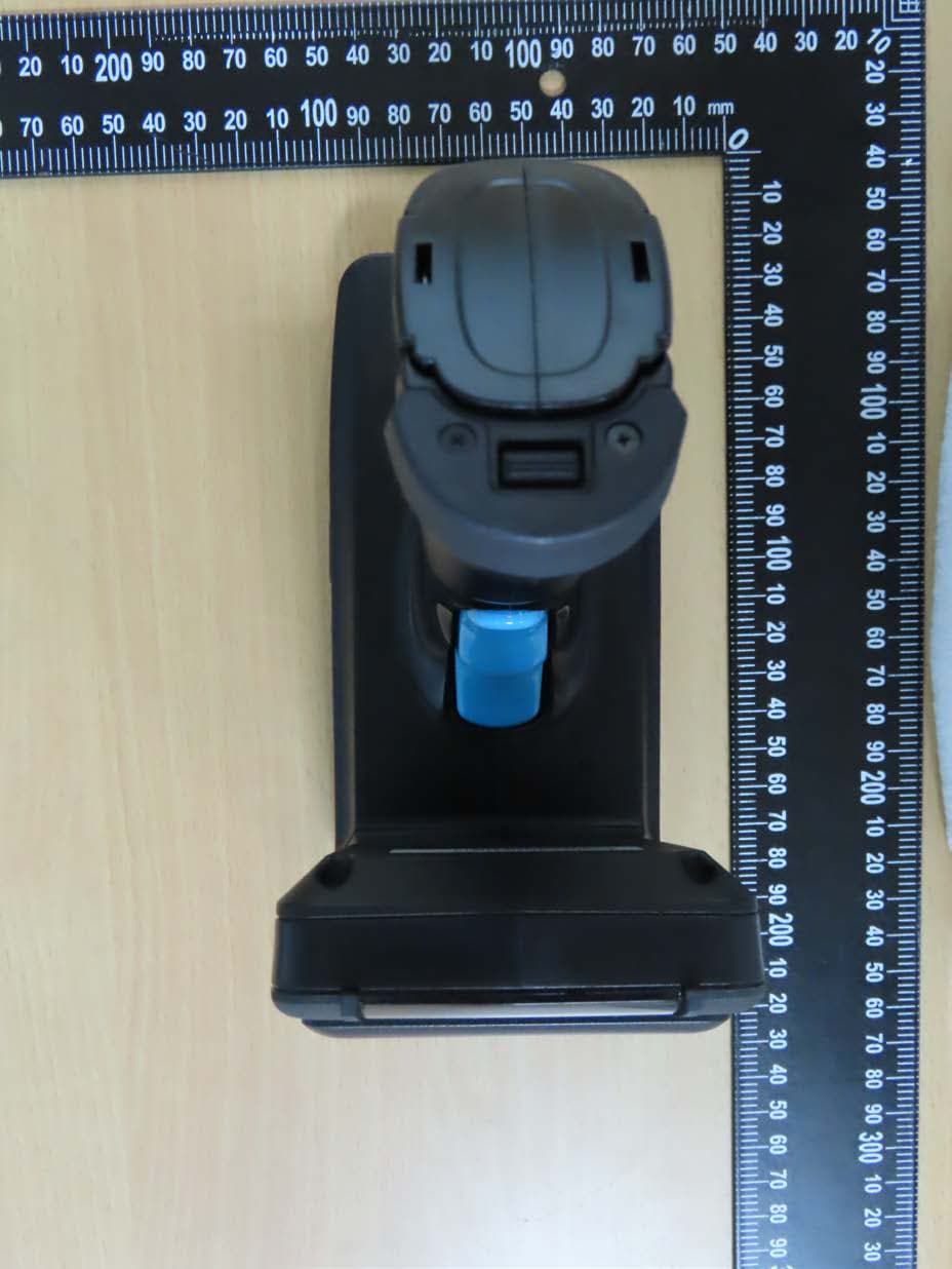
HLERP300BU
Nov 24, 2025RP300 UHF RFID Mobile Reader
Equipment Class
DSS - Part 15 Spread Spectrum Transmitter
HLERM300PU
Sep 01, 2024RM300 Plus UHF RFID Reader Module
Equipment Class
DSS - Part 15 Spread Spectrum Transmitter