JZ2X001700Ribbon RFID
Fargo Electronics Inc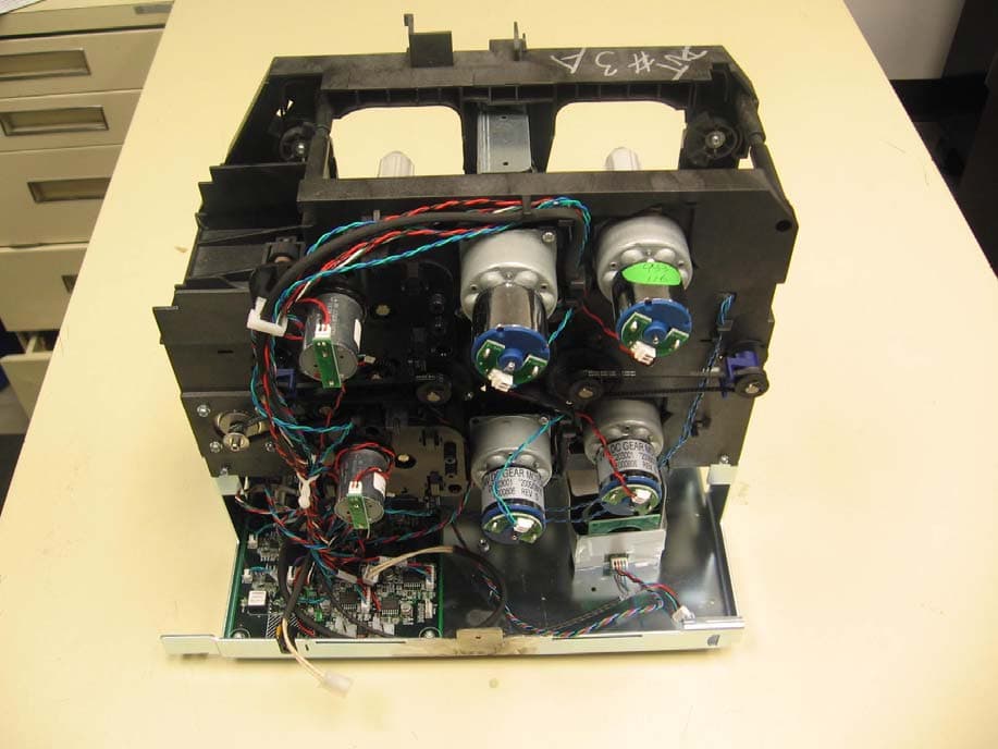
Click to zoom
Application Details
- Equipment Class
- DXX - Part 15 Low Power Communication Device Transmitter
- Date of Grant
- Feb 21, 2007
- Application Purpose
- Original Equipment
- Date of Application
- Feb 21, 2007
- Equipment Note
- Ribbon RFID
- Frequency Range
- 13.55300000 - 13.56700000
- Company
- Fargo Electronics Inc
- Country
- United States
Documents & Files
Document Text
Text extracted from the exhibit documents filed with the FCC. Open a document above to read the original.
Users Manual
HDP100 High Definition Card Printer/Encoder User Guide (Rev. Beta); Sections 1 to 3 (modified) Armstrong 1x (single-Side) Armstrong 2x (dual-Side) Armstrong 1x L (single-side + lamination) Armstrong 2x L (single-side + lamination) Armstrong 2x L (dual-side + lamination) User Guide Part Number: L000950 RESTRICTED USE ONLY Fargo Electronics, Inc. HDP100 High Definition Card Printer/Encoder User Guide (Rev. Beta) ii HDP100 High Definition Card Printer/Encoder User Guide (Rev. Beta), property of Fargo Electronics, Incorporated Copyright 2006 by Fargo Electronics, Incorporated. All rights reserved. Printed in the United States of America. Exclusive permission is granted to authorized resellers of Fargo products to reproduce and distribute this copyrighted document to authorized Fargo customers. The revision number for this document will be updated to reflect changes, corrections, updates and enhancements to this document. Revision Control Number Date Document Title Revision Beta 1 January 2007 HDP100 High Definition Card Printer/Encoder User Guide These reference documents were thoroughly reviewed to provide Fargo with professional and international standards, requirements, guidelines and models for our technical, training and user documentation. At all times, the Copyright Protection Notice for each document was adhered to within our Fargo documentation process. This reference to other documents does not imply that Fargo is an ISO-certified company at this time. ANSI/ISO/ASQ Q9001-2000 American National Standard, (sub-title) Quality Management Systems – Requirements (published by the American Society of Quality, Quality Press, P.O. Box 3005, Milwaukee, Wisconsin 53201-3005) The ASQ ISO 9000:2000 Handbook (editors, Charles A. Cianfrani, Joseph J. Tsiakals and John E. West; Second Edition; published by the American Society of Quality, Quality Press, 625 N. Plankinton Avenue, Milwaukee, Wisconsin 53203) Juran’s Quality Handbook (editors, Joseph M. Juran and A. Blanton Godfrey; Fifth Edition, McGraw-Hill) Any questions regarding changes, corrections, updates or enhancements to this document should be forwarded to: Fargo Electronics, Incorporated Support Services 6533 Flying Cloud Drive Eden Prairie, MN 55344 (USA) (952) 941-9470 FAX: (952) 941-7836 www.fargo.com E-mail: [email protected] RESTRICTED USE ONLY Fargo Electronics, Inc. HDP100 High Definition Card Printer/Encoder User Guide (Rev. Beta) iii Table of Contents Section 1: Printer Overview__________________________________________________1 How to use the guide___________________________________________________________________1 Safety Messages (review carefully)________________________________________________________2 HDP100 Overview____________________________________________________________________3 Reviewing the HDP100 Block Diagram__________________________________________________3 Reviewing the HDP100 Sequence of Operations___________________________________________4 Reviewing the HDP100 Boot up Sequence_______________________________________________7 Reviewing the Lamination Module Sequence of Operations__________________________________8 Reviewing the Lamination Module Boot up Sequence_____________________________________10 Section 2: Specifications_____________________________________________________1 Safety Messages (review carefully)________________________________________________________1 Introduction__________________________________________________________________________2 Reviewing the HDP100 Printer Overview table______________________________________________2 Reviewing the HDP100 Package_______________________________________________________3 Reviewing the HDP100 (front)_________________________________________________________3 Reviewing the HDP100 Card Printer____________________________________________________4 Regulatory Compliances, Agency Listings and FCC Rules_____________________________________5 Regulatory Compliances________________________________________________________________5 Agency Listings_______________________________________________________________________6 FCC Rules________________________________________________________________________6 Technical Specifications________________________________________________________________7 Functional Specifications______________________________________________________________13 Printer Components: Resin Thermal Transfer to USB Interface Port__________________________14 Printer Components: LCD and Softkey Control Pad_______________________________________16 Printer Components: Print Ribbons____________________________________________________21 Printer Components: Blank Cards_____________________________________________________22 Printer Components: Card Input and Output Hoppers______________________________________23 Printer Components: Card Output Hopper and Reject Hopper_______________________________23 Printer Unit: Reviewing the Card Lamination Module_____________________________________24 Printer Components: Transfer Roller___________________________________________________25 Reviewing the Overlaminates___________________________________________________________26 Reviewing the Thermal Transfer Film and PolyGuard Overlaminates__________________________26 Reviewing the CR-80 Patch Size______________________________________________________27 Reviewing the Overlaminate Design___________________________________________________27 Section 3: General Troubleshooting___________________________________________1 LCD Messages_______________________________________________________________________1 Troubleshooting LCD Messages__________________________________________________________2 General Troubleshooting Guide_______________________________________________________14 Magnetic and E-card Troubleshooting Guide_____________________________________________19 Communications Errors________________________________________________________________22 Resolving the Commu…
Text truncated - open the document above for the full version.
Users Manual
HDP100 High Definition Card Printer/Encoder User Guide (Rev. Beta); Sections 1 to 3 (modified) Armstrong 1x (single-Side) Armstrong 2x (dual-Side) Armstrong 1x L (single-side + lamination) Armstrong 2x L (single-side + lamination) Armstrong 2x L (dual-side + lamination) User Guide Part Number: L000950 RESTRICTED USE ONLY Fargo Electronics, Inc. HDP100 High Definition Card Printer/Encoder User Guide (Rev. Beta) ii HDP100 High Definition Card Printer/Encoder User Guide (Rev. Beta), property of Fargo Electronics, Incorporated Copyright 2006 by Fargo Electronics, Incorporated. All rights reserved. Printed in the United States of America. Exclusive permission is granted to authorized resellers of Fargo products to reproduce and distribute this copyrighted document to authorized Fargo customers. The revision number for this document will be updated to reflect changes, corrections, updates and enhancements to this document. Revision Control Number Date Document Title Revision Beta 1 January 2007 HDP100 High Definition Card Printer/Encoder User Guide These reference documents were thoroughly reviewed to provide Fargo with professional and international standards, requirements, guidelines and models for our technical, training and user documentation. At all times, the Copyright Protection Notice for each document was adhered to within our Fargo documentation process. This reference to other documents does not imply that Fargo is an ISO-certified company at this time. ANSI/ISO/ASQ Q9001-2000 American National Standard, (sub-title) Quality Management Systems – Requirements (published by the American Society of Quality, Quality Press, P.O. Box 3005, Milwaukee, Wisconsin 53201-3005) The ASQ ISO 9000:2000 Handbook (editors, Charles A. Cianfrani, Joseph J. Tsiakals and John E. West; Second Edition; published by the American Society of Quality, Quality Press, 625 N. Plankinton Avenue, Milwaukee, Wisconsin 53203) Juran’s Quality Handbook (editors, Joseph M. Juran and A. Blanton Godfrey; Fifth Edition, McGraw-Hill) Any questions regarding changes, corrections, updates or enhancements to this document should be forwarded to: Fargo Electronics, Incorporated Support Services 6533 Flying Cloud Drive Eden Prairie, MN 55344 (USA) (952) 941-9470 FAX: (952) 941-7836 www.fargo.com E-mail: [email protected] RESTRICTED USE ONLY Fargo Electronics, Inc. HDP100 High Definition Card Printer/Encoder User Guide (Rev. Beta) iii Table of Contents Section 1: Printer Overview__________________________________________________1 How to use the guide___________________________________________________________________1 Safety Messages (review carefully)________________________________________________________2 HDP100 Overview____________________________________________________________________3 Reviewing the HDP100 Block Diagram__________________________________________________3 Reviewing the HDP100 Sequence of Operations___________________________________________4 Reviewing the HDP100 Boot up Sequence_______________________________________________7 Reviewing the Lamination Module Sequence of Operations__________________________________8 Reviewing the Lamination Module Boot up Sequence_____________________________________10 Section 2: Specifications_____________________________________________________1 Safety Messages (review carefully)________________________________________________________1 Introduction__________________________________________________________________________2 Reviewing the HDP100 Printer Overview table______________________________________________2 Reviewing the HDP100 Package_______________________________________________________3 Reviewing the HDP100 (front)_________________________________________________________3 Reviewing the HDP100 Card Printer____________________________________________________4 Regulatory Compliances, Agency Listings and FCC Rules_____________________________________5 Regulatory Compliances________________________________________________________________5 Agency Listings_______________________________________________________________________6 FCC Rules________________________________________________________________________6 Technical Specifications________________________________________________________________7 Functional Specifications______________________________________________________________13 Printer Components: Resin Thermal Transfer to USB Interface Port__________________________14 Printer Components: LCD and Softkey Control Pad_______________________________________16 Printer Components: Print Ribbons____________________________________________________21 Printer Components: Blank Cards_____________________________________________________22 Printer Components: Card Input and Output Hoppers______________________________________23 Printer Components: Card Output Hopper and Reject Hopper_______________________________23 Printer Unit: Reviewing the Card Lamination Module_____________________________________24 Printer Components: Transfer Roller___________________________________________________25 Reviewing the Overlaminates___________________________________________________________26 Reviewing the Thermal Transfer Film and PolyGuard Overlaminates__________________________26 Reviewing the CR-80 Patch Size______________________________________________________27 Reviewing the Overlaminate Design___________________________________________________27 Section 3: General Troubleshooting___________________________________________1 LCD Messages_______________________________________________________________________1 Troubleshooting LCD Messages__________________________________________________________2 General Troubleshooting Guide_______________________________________________________14 Magnetic and E-card Troubleshooting Guide_____________________________________________19 Communications Errors________________________________________________________________22 Resolving the Commu…
Text truncated - open the document above for the full version.
Block Diagram
Ribbon RFID system technical description 1. Block diagram with clock frequencies labeled sensors motors serial ports MAIN PCB Ribbon RFID RFID Base 13.56 MHz PCB I-Code 1 Antenna RC400/RC632 24V Power Supply 110-240 VAC
Block Diagram
Ribbon RFID system technical description 1. Block diagram with clock frequencies labeled sensors motors serial ports MAIN PCB Ribbon RFID RFID Base 13.56 MHz PCB I-Code 1 Antenna RC400/RC632 24V Power Supply 110-240 VAC
Operational Description
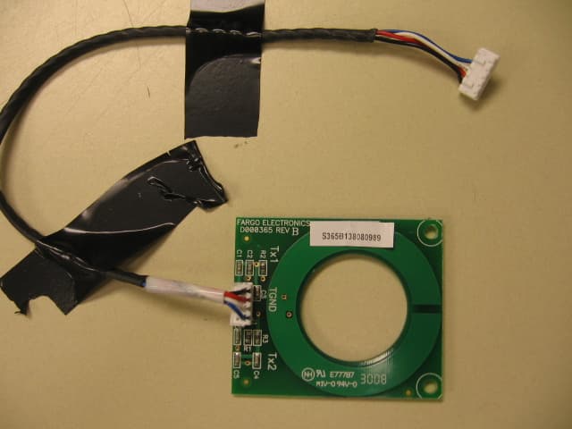
Operational Description 2. Modes of operation There are following modes of operation: RFID standby, and RFID communications between the controller and ribbon RFID tag. During standby mode, RF field is off. RFID is active for 0.2-1 sec. There is RFID tag Read/Write operation going on during this time period. RFID base uses Philips I-CODE1 13.56MHz. Inductive coupling principle is used for RF portion of the system 3. Antenna and ground system description PCB antenna used is a standalone board. It has 4 turns / traces on internal PCB layers, and a shield on external PCB layers (open loop) . The antenna is connected to the base station via 4-wire cable. Also see antenna schematic and PCB layout attached as separate files. The power cord does not have connection to safety ground. PCB antenna size is: 2”x1.75” +24V L Power Main Board PCB GND Supply Antenna N GND GND
Operational Description
Operational Description 2. Modes of operation There are following modes of operation: RFID standby, and RFID communications between the controller and ribbon RFID tag. During standby mode, RF field is off. RFID is active for 0.2-1 sec. There is RFID tag Read/Write operation going on during this time period. RFID base uses Philips I-CODE1 13.56MHz. Inductive coupling principle is used for RF portion of the system 3. Antenna and ground system description PCB antenna used is a standalone board. It has 4 turns / traces on internal PCB layers, and a shield on external PCB layers (open loop) . The antenna is connected to the base station via 4-wire cable. Also see antenna schematic and PCB layout attached as separate files. The power cord does not have connection to safety ground. PCB antenna size is: 2”x1.75” +24V L Power Main Board PCB GND Supply Antenna N GND GND
Schematics
55 44 33 22 11 D D C C B B A A VDD +3_3V VSS +5V GNDGND +5V RFGNDGNDRFGND RFGND VCC GND RFGND RFGND GND RFGND +5V GNDGND RFGND +3_3V GNDGND +3_3V+3_3V +3_3V +3_3V RFGND RFID_RESET {2} RFID_IRQ- {5} RFID_TX1_R {1} RFID_TX2_R {1} RFID_RX_R {1} RFID_TX1_F {1} RFID_TX2_F {1} RFID_RX_F {1} RFID_R+_F- {5} RFID_SPI_SS- {5} RFID_MISO {5} RFID_MOSI {5} RFID_CLK {5} TitleSize Document Number Rev Date: Sheet of Project D000429 B RFID Circuits Fargo Electronics, Inc.Electrical Engineering6533 Flying Cloud DriveEden Prairie, MN. 55344C 13 18 Tuesday, August 08, 2006Armstrong TitleSize Document Number Rev Date: Sheet of Project D000429 B RFID Circuits Fargo Electronics, Inc.Electrical Engineering6533 Flying Cloud DriveEden Prairie, MN. 55344C 13 18 Tuesday, August 08, 2006Armstrong TitleSize Document Number Rev Date: Sheet of Project D000429 B RFID Circuits Fargo Electronics, Inc.Electrical Engineering6533 Flying Cloud DriveEden Prairie, MN. 55344C 13 18 Tuesday, August 08, 2006Armstrong FARGO ELECTRONICS CONFIDENTIAL RIBBON AND FILM RFID RFGND is a portion of the GND plane sectioned off s tarting under U36 and extending around the board header JP1 3. RFGND connects to the GND plane near U36 pin-28. Components located over RFGND ground plane section. Connecting trace width for thesecomponents should be 0.015" minimum. 2%2%2%2%2%2% C155 & C156 & C161 & C162 should tie to RFGND using 3 vias on a small copper pour that starts at the RFGN D end of the capacitors. R320 825 ohm R320 825 ohm D1 4 D2 7 D3 9 D4 12 S1A 2 S1B 3 S2A 5 S2B 6 S3A 11 S3B 10 S4A 14 S4B 13 VDD 16 GND 8 IN 1 /EN 15 U35 ADG774BRQZ U35 ADG774BRQZ C156 47pF C156 47pF Y313.56 MHzY313.56 MHz L3 2.2uH L3 2.2uH C158 27pF C158 27pF C157 27pF C157 27pF C159 15pF C159 15pF C160 0.1uF C160 0.1uF L4 2.2uH L4 2.2uH R318 10.0K R318 10.0K R319 10.0K R319 10.0K C1640.1uFC1640.1uF C162 47pF C162 47pF C1630.1uFC1630.1uF L2 2.2uH L2 2.2uH C16510uFC16510uF L5 2.2uH L5 2.2uH R317 10.0K R317 10.0K R321 4.75K R321 4.75K C155 47pF C155 47pF OSCIN 1 OSCOUT 32 /SS /ALE 21 /CS 9 IRQ 2 /WR 10 /RD 11 MOSI A0 22 A1 23 SCK A2 24 MISO D0 13 D1 14 D2 15 D3 16 D4 17 D5 18 D6 19 D7 20 RX 29 VMID 30 AVSS 28 TX1 5 TVSS 8 TX2 7 MFIN 3 MFOUT 4 RSTPD 31 AUX 27 TVDD 6 AVDD 26 DVDD 25 DVSS 12 U36 CL RC632 U36 CL RC632 C154 15pF C154 15pF C161 47pF C161 47pF
Schematics
55 44 33 22 11 D D C C B B A A VDD +3_3V VSS +5V GNDGND +5V RFGNDGNDRFGND RFGND VCC GND RFGND RFGND GND RFGND +5V GNDGND RFGND +3_3V GNDGND +3_3V+3_3V +3_3V +3_3V RFGND RFID_RESET {2} RFID_IRQ- {5} RFID_TX1_R {1} RFID_TX2_R {1} RFID_RX_R {1} RFID_TX1_F {1} RFID_TX2_F {1} RFID_RX_F {1} RFID_R+_F- {5} RFID_SPI_SS- {5} RFID_MISO {5} RFID_MOSI {5} RFID_CLK {5} TitleSize Document Number Rev Date: Sheet of Project D000429 B RFID Circuits Fargo Electronics, Inc.Electrical Engineering6533 Flying Cloud DriveEden Prairie, MN. 55344C 13 18 Tuesday, August 08, 2006Armstrong TitleSize Document Number Rev Date: Sheet of Project D000429 B RFID Circuits Fargo Electronics, Inc.Electrical Engineering6533 Flying Cloud DriveEden Prairie, MN. 55344C 13 18 Tuesday, August 08, 2006Armstrong TitleSize Document Number Rev Date: Sheet of Project D000429 B RFID Circuits Fargo Electronics, Inc.Electrical Engineering6533 Flying Cloud DriveEden Prairie, MN. 55344C 13 18 Tuesday, August 08, 2006Armstrong FARGO ELECTRONICS CONFIDENTIAL RIBBON AND FILM RFID RFGND is a portion of the GND plane sectioned off s tarting under U36 and extending around the board header JP1 3. RFGND connects to the GND plane near U36 pin-28. Components located over RFGND ground plane section. Connecting trace width for thesecomponents should be 0.015" minimum. 2%2%2%2%2%2% C155 & C156 & C161 & C162 should tie to RFGND using 3 vias on a small copper pour that starts at the RFGN D end of the capacitors. R320 825 ohm R320 825 ohm D1 4 D2 7 D3 9 D4 12 S1A 2 S1B 3 S2A 5 S2B 6 S3A 11 S3B 10 S4A 14 S4B 13 VDD 16 GND 8 IN 1 /EN 15 U35 ADG774BRQZ U35 ADG774BRQZ C156 47pF C156 47pF Y313.56 MHzY313.56 MHz L3 2.2uH L3 2.2uH C158 27pF C158 27pF C157 27pF C157 27pF C159 15pF C159 15pF C160 0.1uF C160 0.1uF L4 2.2uH L4 2.2uH R318 10.0K R318 10.0K R319 10.0K R319 10.0K C1640.1uFC1640.1uF C162 47pF C162 47pF C1630.1uFC1630.1uF L2 2.2uH L2 2.2uH C16510uFC16510uF L5 2.2uH L5 2.2uH R317 10.0K R317 10.0K R321 4.75K R321 4.75K C155 47pF C155 47pF OSCIN 1 OSCOUT 32 /SS /ALE 21 /CS 9 IRQ 2 /WR 10 /RD 11 MOSI A0 22 A1 23 SCK A2 24 MISO D0 13 D1 14 D2 15 D3 16 D4 17 D5 18 D6 19 D7 20 RX 29 VMID 30 AVSS 28 TX1 5 TVSS 8 TX2 7 MFIN 3 MFOUT 4 RSTPD 31 AUX 27 TVDD 6 AVDD 26 DVDD 25 DVSS 12 U36 CL RC632 U36 CL RC632 C154 15pF C154 15pF C161 47pF C161 47pF
Test Report
TEST REPORT Report Number: 3110296MIN-004R Project Number: 3110296 Evaluation of the Ribbon RFID FCC ID: X001700 to FCC Part 2 FCC Part 15, Subpart C, Section 15.225 For Fargo Electronics Inc. Test Performed by: Test Authorized by: Intertek 7250 Hudson Blvd. Suite 100 Oakdale, MN 55128 Fargo Electronics Inc. 6533 Flying Cloud Drive, Suite 1000 Eden Prairie, MN 55344-3307 Prepared by: Date: December 21, 2006 Norman Shpilsher Reviewed by: Date: December 21, 2006 Uri Spector FCC ID: X001700 Report 3110296MIN-004R, December 2006 Page 2 of 21 CONTENTS 1.0 GENERAL DESCRIPTION ............................................................................... 3 1.1 Related Submittals Grants ................................................................................... 3 1.2 Product Description........................................................................................... 3 1.3 Test Methodology............................................................................................. 3 1.4 Test Facility.................................................................................................... 3 2.0 SYSTEM TEST CONFIGURATION .................................................................... 4 2.1 Justification .................................................................................................... 4 2.2 EUT Setup ..................................................................................................... 4 2.3 EUT Exercising Software ................................................................................... 4 2.4 Special Accessories ........................................................................................... 4 2.5 Equipment Modification ..................................................................................... 4 2.6 Support Equipment List and Description.................................................................. 4 2.7 Test Configuration Block Diagrams ....................................................................... 5 3.0 TEST RESULTS ............................................................................................ 6 3.1 Field Strength of Radiated Emissions, FCC 15.225(a)(b)(c), 15.209 ................................ 7 3.2 Out of Band Spurious Emissions, FCC 15.225(d), 15.209 ............................................ 9 3.3 Field Strength of Spurious Emissions, FCC 15.205, 15.209 ......................................... 10 3.4 Frequency Tolerance, FCC 15.225(e).................................................................... 14 3.5 Bandwidth of Emissions, FCC 15.215 ................................................................... 15 3.6 Line Conducted Emissions, FCC 15.207 ................................................................ 17 3.7 Test Procedure................................................................................................ 19 3.8 Field Strength Calculation .................................................................................. 20 3.9 Measurement Uncertainty .................................................................................. 20 4.0 TEST EQUIPMENT .......................................................................................21 FCC ID: X001700 Report 3110296MIN-004R, December 2006 Page 3 of 21 1.0 GENERAL DESCRIPTION 1.1 Related Submittals Grants This is single application of the Ribbon RFID Transmitter for Certification under Part 15 Subpart C. There are no other simultaneous applications . 1.2 Product Description The Ribbon RFID is a RFID transmitter operating at 13.56 MHz under CFR 47:2005, Section 15.225. The Ribbon RFID Transmitter is incorporated in XXXXX Printers and XXXXX Laminators manufactured by Fargo Electronics Inc. The Transmitters are identical for both devices and located on the Main Boards with slight differences in components layout. The intended use of the Ribbon RF ID Transmitter is to generate and transmit a RF signal from the Antenna to the RF ID Tag; the same antenna is used to receive modified by Tag RF signal (inductive coupling). Two identical antennas are used with the transmitter, but only one antenna is used at a time. The Ribbon RF ID Transmitter powered at 120 VAC, 60 Hz through the AC/DC Power Adapter. The Ribbon RF ID Transmitter antenna is an integral antenna located on the separate PCB and connected to the transmitter output via the four-wire Antenna Cable. Sample Submitted: December 4, 2006 Test Work Started: December 4, 2006 Test Work Completed: December 8, 2006 1.3 Test Methodology Emission measurements were performed according to the procedures in ANSI C63.4-2003. All field strength radiated emissions measurements were performed in the semi-anechoic chamber, and for each scan, the procedure for maximizing emissions in were followed. All field strength radiated tests were performed at an antenna to EUT distance of 3 meters, unless stated otherwise in the "Justification Section" of this Application. 1.4 Test Facility The test site facility used to collect the radiated and conducted measurement data is located at 7250 Hudson Blvd., Suite 100, Oakdale, Minnesota. This test facility has been fully described in a report dated on December 2005 submitted to FCC. Please reference the site registration number: 90706, dated December 6, 2005. FCC ID: X001700 Report 3110296MIN-004R, December 2006 Page 4 of 21 2.0 SYSTEM TEST CONFIGURATION 2.1 Justification To demonstrate compliance with FCC requirements of the Ribbon RFID the laminator transmitter was tested with one of two identical antennas connected to the device. 2.2 EUT Setup For simplicity of testing, the transmitter was set to transmit continuously. 2.3 EUT Exercising Software Microsoft Hyper Terminal utility was used to set the transmitter mode of operation from the PC 2.4 Special Accessories There are no special accessories necessary for compliance of these products. 2.5 Equipment Modification No modifications were installed during the t…
Text truncated - open the document above for the full version.
Contact Information
Applicant
Gary M Klinefelter(VP, Technology Development)
Technical Contact
Fargo Electronics, Inc.Leon Gershenovich
[email protected]952-918-8622
6533 Flying Cloud Drive · Eden Prairie, Minnesota · United States
Non-Technical Contact
Fargo Electronics, Inc.John Wilson
[email protected]952-941-9470
Test Firm
Intertek Testing ServicesUri Spector
Technical Specifications
| # | Rule Parts | Frequency Range | Power Output |
|---|---|---|---|
| 1 | 15C | 13.553 MHz - 13.567 MHz | - |
Other Applications from Fargo Electronics Inc
JZ2X001800
Jan 06, 2010Ribbon RFID Encoder
Equipment Class
DXX - Part 15 Low Power Communication Device Transmitter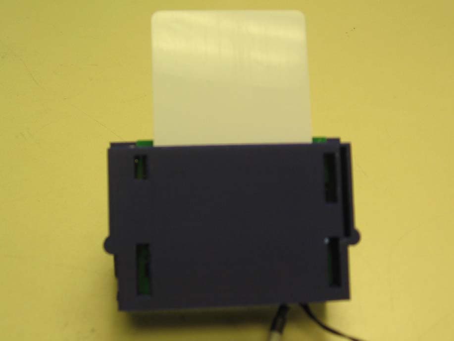
JZ2OMNI5121
Feb 21, 2007Omni Key Reader
Equipment Class
DXX - Part 15 Low Power Communication Device Transmitter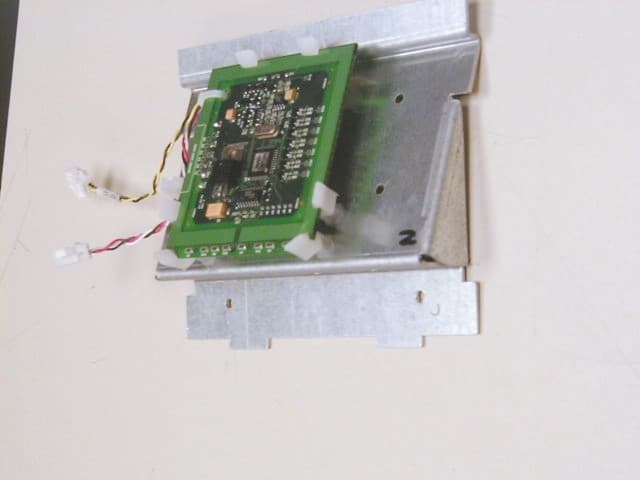
JZ2OEM300
Sep 13, 2005I-Class Encoder
Equipment Class
DXX - Part 15 Low Power Communication Device Transmitter
JZ2X001200
Nov 06, 2002CardJet Card Printer
Equipment Class
DXX - Part 15 Low Power Communication Device TransmitterJZ2-5300X
Jul 26, 1995Printer
Equipment Class
JBP - Part 15 Class B Computing Device Peripheral