KXYPF8400PART 15 CLASS B COMPUTING DEVICE PERIPHERAL
China Great-Wall Computer Shenzhen Co. Ltd.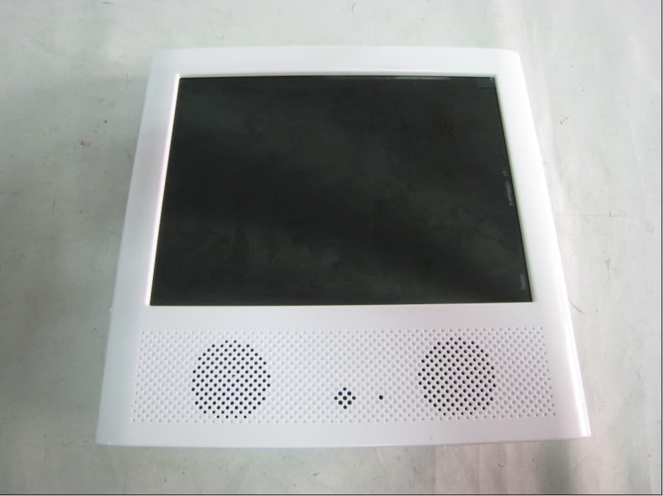
Click to zoom
Application Details
- Equipment Class
- JBP - Part 15 Class B Computing Device Peripheral
- Date of Grant
- Jan 05, 2010
- Application Purpose
- Original Equipment
- Date of Application
- Jan 05, 2010
- Equipment Note
- PART 15 CLASS B COMPUTING DEVICE PERIPHERAL
- Country
- China
Documents & Files
Document Text
Text extracted from the exhibit documents filed with the FCC. Open a document above to read the original.
Users Manual
Federal Communications Commission (FCC) Statement You are cautioned that changes or modifications not expressly approved by the part responsible for compliance could void the user's authority to operate the equipment FCC-Class B This equipment has been tested and found to comply with the limits for a Class B digital device, pursuant to part 15 of the FCC Rules. These limits are designed to provide reasonable protection against harmful interference in a communications. However, there is no guarantee that interference will not occur in particular installation. If this equipment does cause harmful interference to radio or television reception, which can be determined by turning the equipment off and on, the user is encouraged to try to correct the interference by one or more of the following measures: - Reorient or relocate the receiving antenna. - Increase the separation between the equipment and reciver. - Connect the equipment into an outlet on a circuit different from that to which the receiver is connected. - Consult the dealer or an experienced radio/TV technician for help.
Block Diagram
1.2V 3.3V AML6210DP LT1117CST 1117-3.3V DC +5V&12V Digital LCD SDRM-1Mx16bit FLASH-1MBYTE SD CARD AUTO 7 Function KeyUSB Device Battery Clock Controller IC 27MHz Crystal 32.768 KHz Crystal
Cover Letter(s)
China Great-Wall Computer Shenzhen Co., Ltd. Science& Industry Part, Shenzhen, China FCC ID: KXYPF8 400 Power of Attorney 2009- 12-25 Federal Communications Commission Authorization and Evaluation Division 7435 Oakland Mills Road To Whom It May Concern: We, the under signed, hereby authorize Most Technology Service Co., Ltd.(Mark Wen/General Manager) on our behalf, to apply to the Federal Communications Commission on our equipment. Any and all acts carried out by Most Technology Service Co., Ltd.(Mark Wen/General Manager) on our behalf shall have the same effect as acts of our own. This authorization will expire on Dec. 24, 2010. This is to adv ise that we are in full compliance with the Anti-Drug Abuse Act. We, China Great-Wall Computer Shenzhen Co., Ltd. are not subject to a denial of federal benefits pursuant to Section 5301 of the Anti-Drug Act of 1988, 21 USC853a, and no party to the application is subject to a denial of federal benefits pursuant to that section. Sincerely China Great-Wall Computer Shenzhen Co., Ltd. Liu Yu (Enginner)
ID Label/Location Info
Label Location
Operational Description
Operation Principle Digital photo frame was made up of several parts including: CPU, DDR, nor flash, nand flash, t_con, led panel, card reader, USB interface, remote control and power supply. The power supply will power each part for them working, voltage including 5.0V, 3.3V, 12V, 1.2V, all the working instruction is programmed in nor flash. After power supply power so their parts for them working, CPU will get the neither instruction from nor flash and work accordingly. For example, based on the nor flash instruction, CPU will get and decode mp3 file from NAND FLASH, transferring to RGB and PWM signals. The RGB signals will program by T_CON and then will be displayed on LED panel. And the RGB signals will be transferred to voice signal by D/A, which will be amplified before working via loudspeakers. Meanwhile, the ports of car readers or USB interface can make photo frame read more picture files and video & audio files from the capacity device. The end-users can operate digital photo frame via button control or remote control.
Schematics
55 44 33 22 11 D D C C B B A A GND AGND INV_GND 5V Input TO LCD TO Decoder AIC LINPO Vo=1.23*(1+R1/R2) 1128616 LCD_5V SW SW LCD_10V INV_EN LED+ LED- LCD_5V VCC DGND DGND VCC PGND VCC_ADJ DGND LCD_3.3V DAC_3.3V VCC1.2V DGND DGND VCC LCD_10V AGND AGND AGND AGND AGND AGND LCD_5V AGND AGND AGND VGH_15V AGND VGL_-10V LCD_5V +5VA AGND DGND DC_IN INV_EN LED+ LED- TitleSize Document Number Rev Date: Sheet of POWER 1.0 Digital DPF Reference Design using AML6210DP B 211 Monday, August 31, 2009 TitleSize Document Number Rev Date: Sheet of POWER 1.0 Digital DPF Reference Design using AML6210DP B 211 Monday, August 31, 2009 TitleSize Document Number Rev Date: Sheet of POWER 1.0 Digital DPF Reference Design using AML6210DP B 211 Monday, August 31, 2009 + C95 47uF/16V + C95 47uF/16V C310.1UFC310.1UF C29 0.1uF C29 0.1uF D7 DL4001 D7 DL4001 1 2 L2 10uH/CD75100K L2 10uH/CD75100K C70.1uFC70.1uF VCC1V2 TP VCC1V2 TP + C23 47uF/16V + C23 47uF/16V R11 10R R11 10R R49 0R R49 0R R13 10K 1% R13 10K 1% C130.1UFC130.1UF R50 NC R50 NC R14 100K 1% R14 100K 1% CON1dc_powerCON1dc_power 213 U3LT1117CST/ADJU3LT1117CST/ADJ VIN 3 GND 1 VOUT 2 D4 BAV99/BAT54S D4 BAV99/BAT54S 1 3 2 C3347uF/16VC3347uF/16V C20 0.1uF C20 0.1uF C17 0.1UF C17 0.1UF D3 UDZ15B/SOD323 D3 UDZ15B/SOD323 + C21 47uF/16V + C21 47uF/16V R1221.1RR1221.1R FB1 60R/1000mA FB1 60R/1000mA C9 1uf C9 1uf C120.1uFC120.1uF U4 AIC1899(MP1540) U4 AIC1899(MP1540) FB 3 SS 5 LX 1 GND 2 SD 4 IN 6 + C2247uF/16V + C2247uF/16V CON2 2pin/2.3mm CON2 2pin/2.3mm 12 R123 1.2R R123 1.2R FB2 60R/1000mA FB2 60R/1000mA C241uFC241uF C32 0.22Uf C32 0.22Uf C110.1uFC110.1uF R10 200R R10 200R R1522K 1%R1522K 1% L3 10uH/CD75100K L3 10uH/CD75100K C10 47uF/16V C10 47uF/16V J2 2PIN/2MM J2 2PIN/2MM 12 LCD3V3 TP LCD3V3 TP U2 1117-3.3V U2 1117-3.3V VIN 3 ADJ(GND) 1 VOUT 2 R1639K 1%R1639K 1% R12100KR12100K D5 TCUDZS6V8BSOD323 D5 TCUDZS6V8BSOD323 R9 47k R9 47k D8 SS14 D8 SS14 1 2 TP1 GND TP1 GND R19 4.7k R19 4.7k C15 0.1UF C15 0.1UF C18 1uf C18 1uf R121100KR121100K C250.1UFC250.1UF C300.1uFC300.1uF CON9 2pin/1.25mm CON9 2pin/1.25mm 12 DC_IN TP DC_IN TP C3 47uF/16V C3 47uF/16V J12PIN/2MMJ12PIN/2MM 12 U5MP1488(MP3202)U5MP1488(MP3202) FB 3 GND 2 SW 1 OV 5 EN 4 IN 6 VGH TP VGH TP + C28 47uF/16V + C28 47uF/16V D2BAV99/BAT54SD2BAV99/BAT54S 1 3 2 FB3 60R/1000mA FB3 60R/1000mA C1647uF/16VC1647uF/16V LCD10VTPLCD10VTP 1 1 + C27 47uF/16V + C27 47uF/16V C19 47uF/16V C19 47uF/16V D9SS14D9SS14 R8 100R R8 100R D6 DL4001 D6 DL4001 1 2 VGLTPVGLTP C260.1UFC260.1UF R17 0R R17 0R C4 0.1UF C4 0.1UF 55 44 33 22 11 D D C C B B A A Debug I2C,OTG ROM 4x22 NC Debug Options: 22 RP3 NC R29,R32 For software development: JTAG L:512byte M1_CAS_N L:NOR H:16bitH:2048 byte L:GPIO Power On Config:M1_WE_N NAND Boot From Bit Of Flash M1_A10 L:2ALE NAND Flash Page Size H:JTAG EnableH:3ALE L:8bit M1_DQM1 NAND Set Row Address H:NAND M1_RAS_N For ROM LINPO BALL SWITCH = LOW Picture normal display BALL SWITCH = HIGN Picture Rotate Reset Threshold (3.08V) M1_A10M1_DQM1M1_WE_N NAND_CE RESET_N RESET_N AVDD2 NAND_RE LCD_G5LCD_R4 KK2 M1_D0 LCD_B[5:0] LCD_B2LCD_B0 STVL LCD_G2 STHL REXT1 M1_D12 LCD_G[5:0] NAND_CLE M1_D3 LCD_B5LCD_B3LCD_R3 VBUS1 M1_D2 LCD_B1LCD_G1 LCD_R[5:0] OEHOEV M1_D4 LCD_R2 DP1 M1_D1M1_D7 LCD_G0 DM1 M1_BA0 LCD_R0 ID1 M1_D6M1_D13 M1_D[15:8]M1_D[7:0] M1_BA1 M1_RAS_NM1_CAS_N LCD_G4 M1_D8 LCD_R1 M1_DQM1 LCD_R5 AVDD3 M1_D15M1_D14 M1_WE_N LCD_B4 M1_D5M1_D10M1_D9 LCD_G3 CPH1 M1_D11M1_CLK KK1 M1_RAS_NM1_CAS_N AVDD1 M1_DQM0 KK0 M1_SCS0_N M1_A3M1_A1M1_A0M1_A11M1_A4M1_A2M1_A6M1_A7M1_A10M1_A5M1_A9M1_A8 M1_A[11:0] REMOTE IR STVRSTHR TCK TCK TDO TDITMSTDO TMSTDI MUTE CSB BALL_SWITCH BALL_SWITCH IR NAND_ALE NAND_R/BNAND_nWE DAC_3.3V Core1.2V VCC1.2V Core3.3V VCC1.2V Core3.3V Core3.3V AVDD3 USB1.2V AVDD1 AVDD2 USB3.3V Core3.3V Core3.3V Core3.3V Core3.3V Core1.2V USB3.3V Core3.3V Core3.3V Core3.3V DAC_3.3V DGND DGND USB1.2V DAC_3.3V DAC_3.3V Core3.3V M1_A[11:0] 4 M1_WE_N 4 M1_D[7:0] 4 M1_D[15:8] 4 F_nCSF_nOE D_CLK LCD_R[5:0] LCD_G[5:0]LCD_B[5:0] INV_EN M1_BA0 4 NAND_R/BNAND_nWE NAND_CLE 4 M1_BA1 RESET_N KK0KK1KK2 M1_SCS0_N 4 XD_D2/SD_CMD I2C_SDA XD_D3/SD_CLKXD_D4/SD_D0 DM17 ID17 M1_CAS_N 4 XD_D7/SD_D3 OEV XD_D5/SD_D1 M1_DQM1 4 SD/MS/XD_INXD_D6/SD_D2 DP17 M1_DQM0 4 M1_CLK 4 STVL SD/XD_WP STHLOEH CARD_EN VBUS17 M1_RAS_N 4 I2C_SCL STVRSTHR ADATA0/AL ALRCLK ASCLK AMCLK MUTE CSB TitleSize Document Number Rev Date: Sheet of DOCTOR 1.0 Digital DPF Reference Design using AML6210DP C 311 Tuesday, July 28, 2009 TitleSize Document Number Rev Date: Sheet of DOCTOR 1.0 Digital DPF Reference Design using AML6210DP C 311 Tuesday, July 28, 2009 TitleSize Document Number Rev Date: Sheet of DOCTOR 1.0 Digital DPF Reference Design using AML6210DP C 311 Tuesday, July 28, 2009 CON3 Remote_Control CON3 Remote_Control OUT 1 GND 2 VCC 3 C39 0.1UF C39 0.1UF R38 4.7K/NC R38 4.7K/NC FB6 60R/500mA FB6 60R/500mA R373.48K 1%R373.48K 1% RP14*4.7K/NCRP14*4.7K/NC 1 2 3 45 6 7 8 C14210UFC14210UF C53 22PF C53 22PF FB8 60R/500mA FB8 60R/500mA C34 47uF/16V C34 47uF/16V C43 0.1UF C43 0.1UF FB11 60R/500mA FB11 60R/500mA R36 0R R36 0R C75openC75open R30 4.7K/NC R30 4.7K/NC FB9 60R/500mA FB9 60R/500mA C45 0.1UF C45 0.1UF R33 4.7K/NC R33 4.7K/NC R20 100K/NC R20 100K/NC R39 4.7K/NC R39 4.7K/NC FB7 60R/500mA FB7 60R/500mA C35 0.1UF C35 0.1UF C44 0.1UF C44 0.1UF C14010UFC14010UF C48 0.1UF C48 0.1UF C36 0.1UF C36 0.1UF FB5 60R/500mA FB5 60R/500mA R63 1K R63 1K C42 0.1UF C42 0.1UF C64 0.1UF C64 0.1UF R34 4.7K R34 4.7K FB10 60R/500mA FB10 60R/500mA C68 0.1UF C68 0.1UF R35 4.7K R35 4.7K R424.7KR424.7K R27 4.7K/NC R27 4.7K/NC C69 0.1UF C69 0.1UF C51 0.1UF C51 0.1UF C40 0.1UF C40 0.1UF C52 22PF C52 22PF C61 0.1UF C61 0.1UF C109 0.1UF C109 0.1UF R41 4.7K/NC R41 4.7K/NC C59 0.1UF C59 0.1UF C71 15P/NC C71 15P/NC C14110UFC14110UF C67 0.1UF C67 0.1UF R2522RR2522R FB4 60R/1000mA FB4 60R/1000mA C63 0.1UF C63 0.1UF C10110UFC10110UF R32 4.7K/NC R32 4.7K/NC C65 47uF/16V C65 47uF/16V RP24*22RRP24*22R 1 2 3 45 6 7 8 C50 47uF/16V C50 47uF/16V MEMORY PLL JTAG GPIO USB CARD CTON AV POWER U7 AML6210DP/144PI…
Text truncated - open the document above for the full version.
Test Report
Most Technology Service Co., Ltd. Tel:(86) 755-26825180 Fax:(86) 755-86170310 Http:// www. szmost.com Email: [email protected] Test Report Product Name: Digital Photo Frame FCC ID: KXYPF8400 MODEL NO.: PF8400, PF8*** (the first * mean ID code, the second and third mean the customer’s code, * can be 0-9) Applicant: China Great-Wall Computer Shenzhen Co., Ltd. Science&Industry Park,Shenzhen,China Date Received: 12/26/2009 Date Tested: 12/25/2009 Most Technology Service Co., Ltd. Tel:(86) 755-26825180 Fax:(86) 755-86170310 Http:// www. szmost.com Email: [email protected] APPLICANT: China Great-Wall Computer Shenzhen Co., Ltd. FCC ID: KXYPF8400 Page 1 of 10 TABLE OF CONTENTS APPLICANT: China Great-Wall Computer Shenzhen Co., Ltd FCC ID: KXYPF8400 TEST REPORT CONTAINING: PAGE 2...........VERIFICATION OF CONFORMITY PAGE 3-4.........GENERAL INFORMATION PAGE 5...........TEST EQUIPMENT LIST PAGE 6...........TEST PROCEDURE PAGE 7-8.........POWER LINE CONDUCTED INTERFERENCE AND PLOTS PAGE 9-10........RADIATION INTERFERENCE TEST DATA EXHIBIT INCLUDED: PAGE 1...........BLOCK DIAGRAM PAGE 2...........SCHEMATIC PAGE 3...........USERS MANUAL PAGE 4...........LABEL SAMPLE PAGE 5...........LABEL LOCATION PAGE 6...........EXTERNAL PHOTOGRAPHS PAGE 7...........INTERNAL PHOTOGRAPHS PAGE 8...........OPERATIONAL DESCRIPTION PAGE 9...........TEST SET UP PHOTOGRAPHS Most Technology Service Co., Ltd. Tel:(86) 755-26825180 Fax:(86) 755-86170310 Http:// www. szmost.com Email: [email protected] APPLICANT: China Great-Wall Computer Shenzhen Co., Ltd. FCC ID: KXYPF8400 Page 2 of 10 VERIFICATION OF CONFORMITY Equipment Under Test: Digital Photo Frame Brand Name: N/A Model Number: PF8400, PF8*** (the first * mean ID code, the second and third mean the customer’s code, * can be 0-9) FCC ID: KXYPF8400 China Great-Wall Computer Shenzhen Co., Ltd. Applicant: Science&Industry Park,Shenzhen,China China Great-Wall Computer Shenzhen Co., Ltd. Manufacturer: Science&Industry Park,Shenzhen,China Technical Standards: FCC Part 15 B Date of test: Dec. 25, 2009 Deviation: None Condition of Test Sample: Normal The above equipment was tested by MOST for compliance with the requirements set forth in FCC Part 15 and the Technical Standards mentioned above. This said equipment in the configuration described in this report shows the maximum emission levels emanating from equipment and the level of the immunity endurance of the equipment are within the compliance requirements. The test results of this report relate only to the tested sample identified in this report. Tested By Candy Zhang Dec. 26, 2009 Checked By Sam Zhong Dec. 26, 2009 Authorized By Yvette Zhou Dec. 26, 2009 Most Technology Service Co., Ltd. Tel:(86) 755-26825180 Fax:(86) 755-86170310 Http:// www. szmost.com Email: [email protected] APPLICANT: China Great-Wall Computer Shenzhen Co., Ltd. FCC ID: KXYPF8400 Page 3 of 10 GENERAL INFORMATION PRODUCT INFORMATION Housing Type: Plastic EUT Rating Voltage: DC 5V (with Adaptor AC 120V/60Hz) Voltage During Test: DC 5V (with Adaptor AC 120V/60Hz) I/O Type of EUT: DC POWER/Headphone/SD Card/USB/Mini USB I/O Q’TY: 1/1/1/1/1 Model Number: PF8400 Series Number: PF8*** Description of Differences: the first * mean ID code, the second and third mean the customer’s code, * can be 0-9 NOTE: Please refer to the photographs of the EUT. For a more detailed features description about the EUT, please refer to User’s Manual. OBJECTIVE Perform FCC Part 15 Subpart B tests for FCC Marking. TEST STANDARDS AND RESULTS Test items and the results are as bellow: EMISSION Test Item Standard Limits Results Conducted disturbance at mains terminals FCC Subpart 15 B Section 15.107:2008 Class B PASS Radiated disturbance FCC Subpart 15 B Section 15.109:2008 Class B PASS N/A is an abbreviation for Not Applicable. Note: 1. The test result judgment is decided by the limit of measurement standard 2. The information of measurement uncertainty is available upon the customer’s request. Most Technology Service Co., Ltd. Tel:(86) 755-26825180 Fax:(86) 755-86170310 Http:// www. szmost.com Email: [email protected] APPLICANT: China Great-Wall Computer Shenzhen Co., Ltd. FCC ID: KXYPF8400 Page 4 of 10 ENVIRONMENTAL CONDITIONS During the measurement the environmental conditions were within the listed ranges: - Temperature: 15-35ºC - Humidity: 30-60 % - Atmospheric pressure: 86-106 kPa MEASUREMENT UNCERTAINTY The uncertainty is calculated using the methods suggested in the “Guide to the Expression of Uncertainty in Measurement” (GUM) published by ISO. - Uncertainty of Conducted Emission, Uc = ±1.25dB - Uncertainty of Radiated Emission, Uc = ±3.15dB TEST FACILITY Test Site: Most Technology Service Co.,ltd Location: No.5, Langshan 2nd Rd, North Hi-Tech Industrial park, Nanshan Shenzhen, Guangdong, China Description: There is one 3m semi-anechoic an area test sites and two line conducted labs for final test. The Open Area Test Sites and the Line Conducted labs are constructed and calibrated to meet the FCC requirements in documents ANSI C63.4 and CISPR 16 requirements. The FCC Registration Number is 490827. The CNAS Registration Number is CNAS L3573. Site Filing: The site description is on file with the Federal Communications Commission, 7435 Oakland Mills Road, Columbia, MD 21046. Instrument Tolerance: All measuring equipment is in accord with ANSI C63.4 and CISPR 16 requirements that meet industry regulatory agency and accreditation agency requirement. Ground Plane: Two conductive reference ground planes were used during the Line Conducted Emission, one in vertical and the other in horizontal. The dimensions of these ground planes are as below. The vertical ground plane was placed distancing 40 cm to the rear of the wooden test table on where the EUT and the support equipment were placed during test. The horizontal ground plane projected 50 cm beyond the footprint of the EUT system and dist anced 80 cm to the wooden test table. For Radiated Emission Test, one horizontal conductiv…
Text truncated - open the document above for the full version.
Contact Information
Applicant
Lin Yu(Engineer)
86-755-663-9997
Test Firm
Most Technology Service Co., Ltd.Mark Wen
Technical Specifications
| # | Rule Parts | Frequency Range | Power Output |
|---|---|---|---|
| 1 | 15B | - | - |
Other Applications from China Great-Wall Computer Shenzhen Co. Ltd.
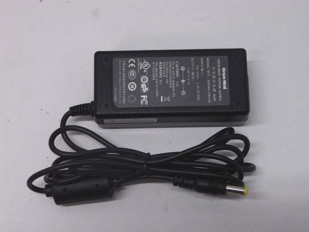
KXY-A892
Dec 09, 2010NOTEBOOK COMPUTER-WLAN PORTION
Equipment Class
DTS - Digital Transmission System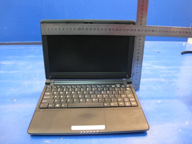
KXYA86
Mar 27, 2010Notebook Computer
Equipment Class
DTS - Digital Transmission System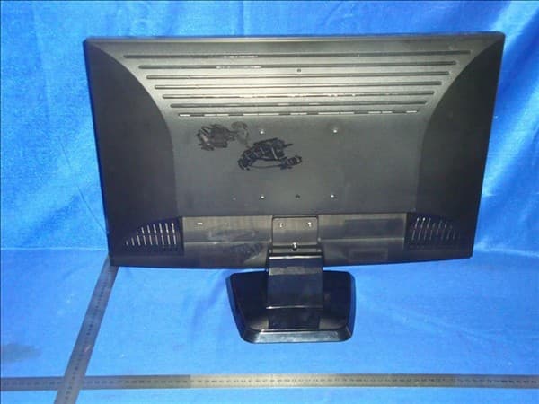
KXYM236XXX
Mar 17, 2010LCD MONITOR
Equipment Class
JBP - Part 15 Class B Computing Device Peripheral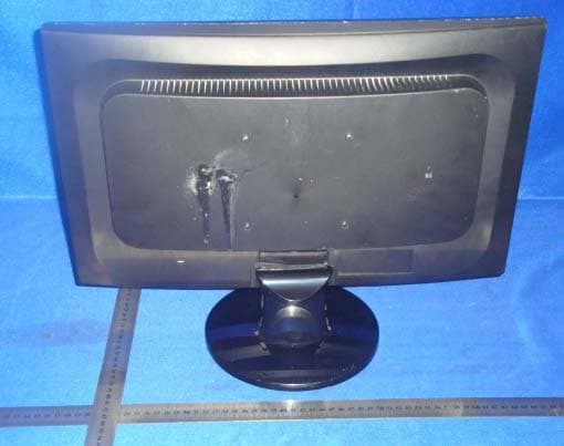
KXYM20DXXX
Jan 18, 2010LCD MONITOR
Equipment Class
JBP - Part 15 Class B Computing Device Peripheral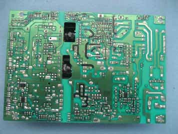
KXYL2632XXXXD
Dec 20, 2007LCD TV
Equipment Class
JBP - Part 15 Class B Computing Device Peripheral