L2C0008TVehicle Alarm Transmitter
APTIV Services US LLC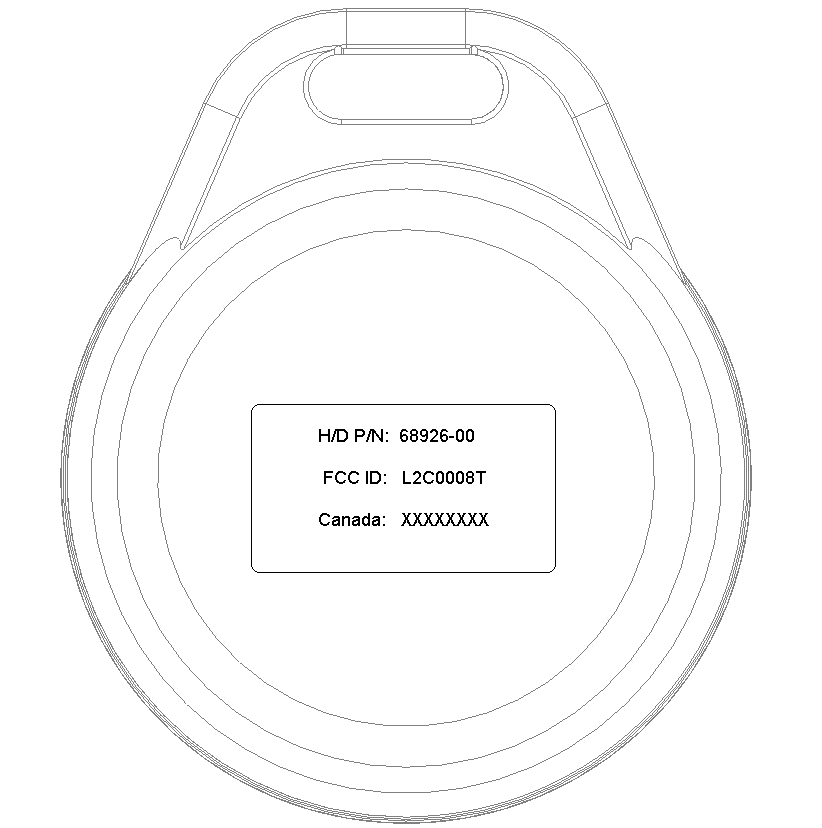
Click to zoom
Application Details
- Equipment Class
- DSC - Part 15 Security/Remote Control Transmitter
- Date of Grant
- Mar 06, 2000
- Application Purpose
- Original Equipment
- Date of Application
- Nov 04, 1999
- Equipment Note
- Vehicle Alarm Transmitter
- Frequency Range
- 315.00000000 - 315.00000000
- Company
- APTIV Services US LLC
- Country
- United States
Documents & Files
Document Text
Text extracted from the exhibit documents filed with the FCC. Open a document above to read the original.
Users Manual
USER’S MANUAL The following statement will be included in the User’s manual: (PRELIMINARY) This device complies with Part 15 of the FCC Rules and with RSS-210 of Industry Canada. Operation is subject to the following two conditions: (1) This device may not cause harmful interference, and (2) This device must accept any interference received, including interference that may cause undesired operation. WARNING: Changes or modifications not expressively approved by the party responsible for compliance could void the user’s authority to operate the equipment.
Attestation Statements
FCC AUTHORIZATION November 1, 1999 To:FCC Authorization & Evaluation Division 7435 Oakland Mills Road Columbia, MD 21045-049 From:Curtis KellPhone: 414-768-2824 Sr. Development EngineerFax:414-768-2820 Applicant: Delphi Automotive SystemsEmail: [email protected] ____________________________________________________________________________ Dear Ladies & Gentlemen: I appoint Kenneth L. Boston and James Blaha at L.S. Compliance, Inc. to act as an agent in the preparation under Part 15 of the rules and regulations of the Federal Communications Commission. I certify that the exhibitions properly describe the device being submitted under this application and will implement any changes described in the test report. The labels described will be affixed to each item. The following statement is required by the Federal Communications Commission: By checking Yes, the applicant certifies that, in the case of an individual applicant, he or she is not subject to a denial of federal benefits, that included FCC benefits, pursuant to section 5301 of the Anti-Drug Abuse Act of 1988, 21 U.S.C. 853(a), or, in the case of a non-individual applicant (e.g. corporation, partnership, or other unincorporated association), no party to the applicant is subject to a denial of federal benefits, that includes FCC benefits, pursuant to that section. __X__ YES____ NO Dated this 1 st day of November, 1999 By:Curtis Kell Title:Sr. Development Engineer Phone:414-768-2824 7929 South Howell Ave. Oak Creek, WI 53154
External Photos
TSSM FOB Front View
External Photos
TSSM FOB Back View
External Photos
TSSM FOB Back Cover Label Detail (self-adhesive label)
External Photos
TSSM FOB Back View Please note... This photo does not include a label. After production, an adhesive label will be attached. Please see label file for label characteristics with FCC and Canada ID Numbers.
External Photos
TSSM FOB Back Cover Label Detail (Self-adhesive label) Please note... This is the adhesive label to be attached to the FOB. Canada ID number to be assigned by Canada.
Internal Photos
TSSM FOB Internal View
Internal Photos
TSSM FOB Circuit Board Top View
Internal Photos
TSSM FOB Circuit Board Bottom View
Operational Description
THEORY OF OPERATION TSSM FOB Transmitter Overview The TSSM FOB transmitter is used in conjunction with a vehicle mounted receiver to provide remote arming and disarming of a vehicle alarm system. The TSSM system is installed on various platforms of Harley Davidson motorcycles. Circuit Theory The transmitter provides a rolling code type of secure RF link based on a Delphi proprietary algorithm. The TSSM transmitter uses the Microchip PIC12C509A microcontroller to decode keypad inputs, generate the appropriate function code and encryption data, and provide a complete digital message stream to the RF output stage. The RF output stage is a single stage transistor SAW based colpits oscillator operating at 315Mhz +/- 100Khz. The antenna is a circuit board trace. Transmitter Block Diagram
Operational Description
TSSM Receiver Theory of Operation The Turn Signal Security System Module (TSSM) is intended for commercial use in various vehicle platforms of Harley Davidson motorcycles starting in model year 2001. This system is comprised of two components. The TSSM receiver module and a hand-held transmitter (FOB). The TSSM system provides several functions on the motorcycle such as turn signal control and cancellation, engine immobilization, security alarm functions including a remote arm /disarm feature. Remote System Functionality The TSSM system consists of a hand-held fob transmitter used by the driver and a TSSM receiver box located on the motorcycle. The transmitter emits RF signals in response to the activation the button on the fob. Upon activation of a fob button, a message is formed and then transmitted. This FOB has been designed to automatically deactivate the transmitter within 5 seconds of the manual switch being released. ( see 47 CFR - Part 15.231 (a) 1. ) The receiver periodically checks for the presence of a transmission. When a valid a message is received, the receiver performs the requested function; either arming or disarming the security syste. The TSSM receiver features a super-regenerative AM receiver. The receiver is tuned to a center frequency of 315 MHz. RF messages are received via an internal wire antenna. The software periodically polls for a message. If a valid RF message is not detected, the RF receiver is switched to a sleep mode to conserve conserve parasitic current. The super-regenerative receiver is composed of an antenna, RF power switching transistor, front end 315 MHz tuned amplifier, super-regenerative stage, diode detector, backend amplifier, and data slice waveshaper. The backend amplifier and waveshaper are implemented using two halves of a dual LM2904 op amp package. Receiver Overview The RF receiver receives and demodulates the incoming 315 Mhz amplitude modulated (AM) RF signals. An internal antenna receives the incoming signals from the transmitter, the signals are amplified through a tuned amplifier, the superregenerative circuit demodulates the 315 Mhz signal and an audio amplifier amplifies the signal which is then sent to the RF microprocessor for data processing (decoding). The receiver has a direct inject sensitivity of approximately 2 uV. Refer to the RF receiver block diagram. The data sent to the RF microprocessor uses a rolling code algorithm for security. RF Front End Amplifier The RF amplifier is mechanized using a transistor in a common emitter configuration with a tuned LC circuit in the collector path to provide selectivity at 315 Mhz. The output of the amplifier is AC coupled to the superregenerative circuit. Superregenerative Circuit The superregenerative circuit is used to demodulate the incoming 315 Mhz signal to a baseband format. The circuit is consists of an RF oscillator operating at 315 Mhz which alternates between an oscillating and non-oscillating condition at a rate known as the quench frequency. When an RF signal (315 Mhz) is applied to the superregenerative circuit, the RF oscillator reaches an oscillating condition faster than when an RF signal is not applied, effectively increasing the quench frequency. The stronger the RF signal, the faster the RF oscillator begins operating. The output of the superregenerative circuit is essentially the variable quench frequency, nominally 600 Khz. The RF oscillator is tuned with a variable inductor which is part of a LC tank circuit. The inductor is adjusted to get maximum sensitivity at 315 Mhz. Nominal bandwidth of the superregenerative circuit id 2.5 Mhz (+/- 3dB). Peak Detect/Low Pass Filter Circuit The output of the superregenerative circuit is sent to the peak detect/low pass filter circuit to demodulate the variable frequency quench oscillation. The output of this circuit is the basedband data (nominally 2 Khz) transmitted by the FOB. Audio Amplifier The low level output of the peak detect/low pass filter circuit is amlified by the audio amplifier comparator circuit. The output of the comparator is sent to the RF uP for signal processing. RF Receiver Block Diagram Front End Amplifier Superregenerative Circuit Peak Detect/Low Pass Filter Circuit Audio Amplifier To RF microprocessor for signal processing
Operational Description
DELPHI Electronics; TSSM , FCC ID: L2C0008T ---------------------------------------------------------------------------------------------------------------------------------------------- Page 1 of 13 DUTY CYCLE CORRECTION FACTOR, CALCULATIONS COPIED FROM REPORT: For a graphical presentation of the data bursts being transmitted from the transmitter, refer to Appendix C. for a zero span picture of the modulation burst from one representative unit. Plots are provided that show the repeating burst of data that occurs when a key is held down continuously, and also over a 250 millisecond (worst case) period and a 20 millisecond period, to display the individual pulses in detail.. The Data is Pulse Position modulated. When the total On-time is computed over a100 millisecond window, according to FCC Part 15.35(c), where the packet duration exceeds 100 milliseconds, a total of 22.87 milliseconds is obtained. This results in a relaxation factor of 12.8 dB, which is under the allowable cap of 20 dB, as stated in FCC Part 15.35(b) The construction of the entire data packet is as follows: Portion duration max on-time Preamble:175 ms.29.167 ms Header :8 ms.1.67 ms. Data: 70.4ms 17.6 ms Total253.4ms48.43ms Selecting the worst case, 100 millisecond window, which is found to be the end of the packet: Portion duration max on-time Preamble:21.6 ms.3.6 ms Header :8 ms.1.67 ms. Data: 70.4ms 17.6 ms Total100 ms22.87 ms Relaxation Factor= 20 log (22.87/100) = 12.8 dB ADDITIONAL INFORMATION REGARDING DUTY CYCLE CORRECTION FACTOR: For the pulse position modulation scheme: A logic "0" is defined by a 0.2 millisecond wide pulse, followed by a 0.6 millisecond dead time. (25% on) A logic "1" is defined by a 0.2 millisecond wide pulse, followed by a 1.0 millisecond dead time. (16.6% on) The Preamble consists of 146 bits, all of the bits are logic "1"s, for a total length of 175.2 ms The Header consists of 8 bits, 4 are logic "1" and 4 are logic "0", for a length of 8 ms. The Data consists of 88 bits, which are mixed "0"s and "1"s. All "0"s results in 70.4 ms length. Since this is a pulse position modulation scheme, and because the third section of the packet can vary in composition, the total length can vary from about 250 ms. to 288 ms. For the calculation presented in the report, and reiterated above, the worst case packet, where the bits in the data section are all set to be a logic "0", was utilized. DELPHI Electronics; TSSM , FCC ID: L2C0008T ---------------------------------------------------------------------------------------------------------------------------------------------- Page 2 of 13 On the following pages can be found a number of oscilloscope traces, showing greater detail of the data packet construction of a sample keyfob. These were created by connecting the oscilloscope input to the video (baseband, or detected) output of a spectrum analyzer. The transmit signal from the sample was picked up by a near field probe, (Emco H-field loop) and coupled into the spectrum analyzer input. The keyfob transmitter button was then depressed, and the resulting data packet was captured in the oscilloscope memory, and resultant close-up scans were directly transferred to disc, and imported as .TIF files to this document. There are two things to keep in mind: 1. The timing, or clock in the transmitter is RC based, and is not exact, and can drift, which will effect the on-times and off times. 2. The packet details shown are for a typical sample, and do not represent the worst case. This means that the data section, which is the last 88 bits, are a combination of logic "0"s and logic "1"s, which will cause the length of this section to increase beyond 70.4 ms. The general effect of this is to cause the duty cycle to vary by a few percent, but in the general direction of a lower duty cycle than that derived in the calculations. The packet shown in detail in the following graphs is about 290 milliseconds long, which illustrates the effect of both of the above mentioned variable parameters. View of the Agilent (HP) model 54624A 100 MHz digital oscilloscope; HP 8591EM spectrum analyzer; and EMCO 7405-901 6 centimeter H field probe, used to create the data packet detail plots. DELPHI Electronics; TSSM , FCC ID: L2C0008T----------------------------------- ----------------------------------------------------------------------------------------------------------- Page 3 of 13 20 millisecond window, showing detail at front of the packet transmission, (start of packet occurs 1 cm from left) DELPHI Electronics; TSSM , FCC ID: L2C0008T----------------------------------- ----------------------------------------------------------------------------------------------------------- Page 4 of 13 10 millisecond window, showing detail at front of the packet transmission DELPHI Electronics; TSSM , FCC ID: L2C0008T----------------------------------- ----------------------------------------------------------------------------------------------------------- Page 5 of 13 2 millisecond window, showing detail from near back end of the packet transmission, logic "1" detail DELPHI Electronics; TSSM , FCC ID: L2C0008T----------------------------------- ----------------------------------------------------------------------------------------------------------- Page 6 of 13 2 millisecond window, showing detail from near the back end of the packet transmission, logic "0" detail DELPHI Electronics; TSSM , FCC ID: L2C0008T----------------------------------- ----------------------------------------------------------------------------------------------------------- Page 7 of 13 20 millisecond window, showing detail at middle of the packet transmission, 120ms to 100ms from the back end. All pulses here and ahead of this point in the packet are identical and are part of the preamble. (logic 1) DELPHI Electronics; TSSM , FCC ID: L2C0008T----------------------------------- --------------------------------------------------------------------------------------…
Text truncated - open the document above for the full version.
Schematics
SCHEMATIC TSSM FOB TRANSMITTER
Test Report
LSC _ DELPHI 90248bpageof 24 0 . . . . . . . . . . . . . . . . . . . L. S. Compliance, Inc. Compliance Testing of: DELCO/ DELPHI TSSM, HARLEY DAVIDSON NORTH AMERICA KEYLESS ENTRY TRANSMITTER Prepared for: Curt Kell Delphi Electronics Oak Creek, WI Test Report Number: 90248B Date(s) of Testing: September 17, 20, 1999 L. S. Compliance, Inc. W66 N220 Commerce Court Cedarburg, Wisconsin 53012 Phone: 414 - 375 - 4400 Fax: 414 - 375 - 4248 LSC _ DELPHI 90248bpageof 24 1 All results of this report relate only to the items that were tested. This report may not be reproduced, except in full, without written approval of L. S. Compliance, Inc. L. S. COMPLIANCE, Inc. FCC ID: L2C0008T LSC _ DELPHI 90248bpageof 24 0 Table of Contents SectionDescriptionPage # Index1 Description of Measurement Facilities2 1.2Signature Page3 1.3Summary of Test Report4 1.4Introduction5 1.5Purpose5 1.6Radiated Emission Test Setup5 1.7Radiated Emission Test Procedure6 1.8Radiated Emission Test Equipment Utilized7 1.9Conducted Emission Measurements7 1.10Restricted Bands (Frequencies and Limits)8 1.11Photos taken during testing9 1.12Summary of Results and Conclusions10 1.13Test Equipment List11 Appendic es ASample Calculations:12 i.Calculation of Radiated Emissions Limits13 ii.Duty Cycle Correction Factor Calculation14 iii.Occupied Bandwidth Calculations15 BData Charts16 CGraphs18 L. S. COMPLIANCE, Inc. FCC ID: L2C0008T LSC _ DELPHI 90248bpageof 24 1 DESCRIPTION OF MEASUREMENT FACILITIES Site on File with the FCC ID Number: 31040/SIT 1300F2 “ The site referenced above has been found to comply with the test site criteria found in ANSI C63.4-1992 and 47CFR Section 2.948.” L. S. COMPLIANCE, Inc. FCC ID: L2C0008T LSC _ DELPHI 90248bpageof 24 2 L. S. COMPLIANCE, Inc. FCC ID: L2C0008T LSC _ DELPHI 90248bpageof 24 3 SIGNATUREPAGE Tests performed by: Approved By:9 Nov 1999 Kenneth L. Boston, EMC Lab ManagerDate PE #31926 Registered Professional Engineer (State of Wisconsin) L. S. COMPLIANCE, Inc. FCC ID: L2C0008T LSC _ DELPHI 90248bpageof 24 4 1.3 SUMMARY OF TEST REPORT MANUFACTURER:Delphi Electronics MODEL:T.S.S.M., Harley Davidson North America SERIAL:preproduction prototype DESCRIPTION:KEYLESS ENTRY HANDHELD TRANSMITTER FREQUENCY RANGE:TRANSMITTER; 315 MHz The Delphi model TSSM RKE transmitter was found to “meet” the radiated emission specification of Title 47 CFR FCC, Part 15, subpart C. for an intentional radiator L. S. COMPLIANCE, Inc. FCC ID: L2C0008T LSC _ DELPHI 90248bpageof 24 5 1.4 INTRODUCTION On September 17, 20 of 1999, a series of Radiated Emissions tests were performed on two sample models of the TSSM keyless entry transmitter, a small handheld key fob unit, which is designed to transmit a coded signal used to allow a person to operate their Motorcycle. These tests were performed using the test procedures outlined in ANSI C63.4-1992 for intentional radiators, and in accordance with the limits set forth in FCC Part 15.231a,b for a periodic transmitter. These tests were performed by Kenneth L. Boston, PE, of L. S. Compliance, Inc. and witnessed by Curt Kell of Delphi, Inc. 1.5PURPOSE The above mentioned tests were performed in order to determine the compliance of the TSSM keyfob with limits contained in various provisions of Title 47 CFR, FCC Part 15, including: 15.10915.231b 15.20515.231c 15.209 All radiated emissions tests were performed to measure the emissions in the frequency bands described by the above sections, and to determine whether said emissions are below the limits established by the above sections. These tests were performed in accordance with the procedure described in the American National Standard for methods of measurement of Radio-Noise Emissions from Low-Voltage Electrical and Electronic Equipment in the Range of 9 kHz to 40 GHz (ANSI C63.4-1992). Another document used as reference for the EMI receiver specification was the International Special Committee on Radio Interference (CISPR) number 16-1 (1993). 1.6 RADIATED EMISSIONS TEST SETUP The test samples were operated within the 3 meter Semi-Anechoic, FCC listed chamber located at L.S. Compliance in Cedarburg, WI. The samples were placed on an 80cm high wooden pedestal, which was centered on the flush-mounted 2m diameter metal turntable. The test sample was operated on its own [new] internal battery. The battery voltage at the beginning of the tests was measured to be 3.2 volts. One test sample was configured to run in a continuous transmit mode during the 15.231c and 15.231b measurements. The other test sample was configured to transmit a continuous carrier. Please refer to Section 1.11 for pictures of the test setup. L. S. COMPLIANCE, Inc. FCC ID: L2C0008T LSC _ DELPHI 90248bpageof 24 6 1.7 RADIATED EMISSION TEST PROCEDURE The fundamental and spurious (harmonic) emissions of the transmitter were tested for compliance to Title 47 CFR, FCC Part 15.231b limits for periodic devices. For the calculations used to determine the limits applicable for each of the two test samples (at their respective operating frequencies) refer to Appendix A. These limits are expressed in decibels (dB) above 1 microvolt per meter (μV/m). The samples were tested from the lowest frequency generated by the transmitter (without going below 9 kHz) to the 10th harmonic of the fundamental frequency generated by the device. The appropriate limits were also observed when the fundamental or spurious signals were located within any of the restricted bands as described in Part 15.205a. These frequencies, and their associated limits, are referenced in Section 1.10. The samples were placed on a nonconductive (wooden) pedestal in the 3 Meter chamber and the antenna mast was placed such that the antenna was 3m from the test object. A biconical antenna or tuned dipole was used to measure emissions from 30 to 200 MHz, a log periodic or tuned dipole was used to measure emissions from 200 to 1000 MHz, and a double ridged waveguide horn was used to measure emissions above 1 GHz. The test obje…
Text truncated - open the document above for the full version.
Test Report
LSC _ DELPHI 90248bpageof 24 0 . . . . . . . . . . . . . . . . . . . L. S. Compliance, Inc. Compliance Testing of: DELCO/ DELPHI TSSM, HARLEY DAVIDSON NORTH AMERICA KEYLESS ENTRY TRANSMITTER Prepared for: Curt Kell Delphi Electronics Oak Creek, WI Revised (see highlights) 1 Feb, 2000 Test Report Number: 90248B Date(s) of Testing: September 17, 20, 1999 L. S. Compliance, Inc. W66 N220 Commerce Court Cedarburg, Wisconsin 53012 Phone: 414 - 375 - 4400 Fax: 414 - 375 - 4248 LSC _ DELPHI 90248bpageof 24 1 All results of this report relate only to the items that were tested. This report may not be reproduced, except in full, without written approval of L. S. Compliance, Inc. L. S. COMPLIANCE, Inc. FCC ID: L2C0008T LSC _ DELPHI 90248bpageof 24 0 Table of Contents SectionDescriptionPage # Index1 Description of Measurement Facilities2 1.2Signature Page3 1.3Summary of Test Report4 1.4Introduction5 1.5Purpose5 1.6Radiated Emission Test Setup5 1.7Radiated Emission Test Procedure6 1.8Radiated Emission Test Equipment Utilized7 1.9Conducted Emission Measurements7 1.10Restricted Bands (Frequencies and Limits)8 1.11Photos taken during testing9 1.12Summary of Results and Conclusions10 1.13Test Equipment List11 Appendic es ASample Calculations:12 i.Calculation of Radiated Emissions Limits13 ii.Duty Cycle Correction Factor Calculation14 iii.Occupied Bandwidth Calculations15 BData Charts16 CGraphs18 L. S. COMPLIANCE, Inc. FCC ID: L2C0008T LSC _ DELPHI 90248bpageof 24 1 DESCRIPTION OF MEASUREMENT FACILITIES Site on File with the FCC ID Number: 31040/SIT 1300F2 “ The site referenced above has been found to comply with the test site criteria found in ANSI C63.4-1992 and 47CFR Section 2.948.” L. S. COMPLIANCE, Inc. FCC ID: L2C0008T LSC _ DELPHI 90248bpageof 24 2 L. S. COMPLIANCE, Inc. FCC ID: L2C0008T LSC _ DELPHI 90248bpageof 24 3 SIGNATUREPAGE Tests performed by: Approved By:9 Nov 1999 Kenneth L. Boston, EMC Lab ManagerDate PE #31926 Registered Professional Engineer (State of Wisconsin) L. S. COMPLIANCE, Inc. FCC ID: L2C0008T LSC _ DELPHI 90248bpageof 24 4 1.3 SUMMARY OF TEST REPORT MANUFACTURER:Delphi Electronics MODEL:T.S.S.M., Harley Davidson North America SERIAL:preproduction prototype DESCRIPTION:KEYLESS ENTRY HANDHELD TRANSMITTER FREQUENCY RANGE:TRANSMITTER; 315 MHz The Delphi model TSSM RKE transmitter was found to “meet” the radiated emission specification of Title 47 CFR FCC, Part 15, subpart C. for an intentional radiator L. S. COMPLIANCE, Inc. FCC ID: L2C0008T LSC _ DELPHI 90248bpageof 24 5 1.4 INTRODUCTION On September 17, 20 of 1999, a series of Radiated Emissions tests were performed on two sample models of the TSSM keyless entry transmitter, a small handheld key fob unit, which is designed to transmit a coded signal used to allow a person to operate their Motorcycle. These tests were performed using the test procedures outlined in ANSI C63.4-1992 for intentional radiators, and in accordance with the limits set forth in FCC Part 15.231a,b for a periodic transmitter. These tests were performed by Kenneth L. Boston, PE, of L. S. Compliance, Inc. and witnessed by Curt Kell of Delphi, Inc. 1.5PURPOSE The above mentioned tests were performed in order to determine the compliance of the TSSM keyfob with limits contained in various provisions of Title 47 CFR, FCC Part 15, including: 15.10915.231b 15.20515.231c 15.209 All radiated emissions tests were performed to measure the emissions in the frequency bands described by the above sections, and to determine whether said emissions are below the limits established by the above sections. These tests were performed in accordance with the procedure described in the American National Standard for methods of measurement of Radio-Noise Emissions from Low-Voltage Electrical and Electronic Equipment in the Range of 9 kHz to 40 GHz (ANSI C63.4-1992). Another document used as reference for the EMI receiver specification was the International Special Committee on Radio Interference (CISPR) number 16-1 (1993). 1.6 RADIATED EMISSIONS TEST SETUP The test samples were operated within the 3 meter Semi-Anechoic, FCC listed chamber located at L.S. Compliance in Cedarburg, WI. The samples were placed on an 80cm high wooden pedestal, which was centered on the flush-mounted 2m diameter metal turntable. The test sample was operated on its own [new] internal battery. The battery voltage at the beginning of the tests was measured to be 3.2 volts. One test sample was configured to run in a continuous transmit mode during the 15.231c and 15.231b measurements. The other test sample was configured to transmit a continuous carrier. Please refer to Section 1.11 for pictures of the test setup. L. S. COMPLIANCE, Inc. FCC ID: L2C0008T LSC _ DELPHI 90248bpageof 24 6 1.7 RADIATED EMISSION TEST PROCEDURE The fundamental and spurious (harmonic) emissions of the transmitter were tested for compliance to Title 47 CFR, FCC Part 15.231b limits for periodic devices. For the calculations used to determine the limits applicable for each of the two test samples (at their respective operating frequencies) refer to Appendix A. These limits are expressed in decibels (dB) above 1 microvolt per meter (μV/m). The samples were tested from the lowest frequency generated by the transmitter (without going below 9 kHz) to the 10th harmonic of the fundamental frequency generated by the device. The appropriate limits were also observed when the fundamental or spurious signals were located within any of the restricted bands as described in Part 15.205a. These frequencies, and their associated limits, are referenced in Section 1.10. The samples were placed on a nonconductive (wooden) pedestal in the 3 Meter chamber and the antenna mast was placed such that the antenna was 3m from the test object. A biconical antenna or tuned dipole was used to measure emissions from 30 to 200 MHz, a log periodic or tuned dipole was used to measure emissions from 200 to 1000 MHz, and a double ridged waveguide horn was used to measure…
Text truncated - open the document above for the full version.
Contact Information
Applicant
Brian W Johnson(Engineering Group Manager)
Technical Contact
Delphi Delco Electronics SystemsCurtis Kell
[email protected]414 - 768 - 2824
7929 South howell avenue · Oak Creek, Wisconsin · United States
Non-Technical Contact
L. S. Compliance, Inc.James Blaha
[email protected]262-375-4400
Test Firm
L. S. Compliance, Inc.James Blaha
262-375-4400Fax: 262-375-4248
Technical Specifications
| # | Rule Parts | Frequency Range | Power Output |
|---|---|---|---|
| 1 | 15C | 315 MHz - 315 MHz | - |
Other Applications from APTIV Services US LLC
L2CSRR6PS
Apr 09, 2024SRR6PS
Equipment Class
VRD - Part 95 Vehicular Radar SystemsL2C0093TR
Mar 12, 2024Wireless Charging Module
Equipment Class
8CC - Part 18 Consumer Device
L2C0090TR
Oct 04, 2023Passive entry Keyless Go with tire pressure and door handle monitoring radio frequency module
Equipment Class
DCD - Part 15 Low Power Transmitter Below 1705 kHz
L2C0089TR
Jun 05, 2023FO3-TR903BDA
Equipment Class
DSC - Part 15 Security/Remote Control Transmitter
L2C0084TR
Jul 27, 2021Wireless Power Transfer Charger
Equipment Class
8CC - Part 18 Consumer Device