LBBFF2100HT900MHz 40 Channel Analog Modulation Cordless Phone
Continental Conair Limited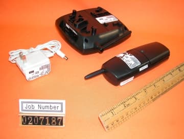
Click to zoom
Application Details
- Equipment Class
- DXT - Part 15 Low Power Transceiver, Rx Verified
- Date of Grant
- Aug 19, 2002
- Application Purpose
- Original Equipment
- Date of Application
- Aug 19, 2002
- Equipment Note
- 900MHz 40 Channel Analog Modulation Cordless Phone
- Frequency Range
- 926.11700000 - 927.28800000
- Company
- Continental Conair Limited
- Country
- Hong Kong
Documents & Files
Document Text
Text extracted from the exhibit documents filed with the FCC. Open a document above to read the original.
Block Diagram
FF2100bbd.sch-1 - Sat Aug 03 09:03:21 2002 FF2100hbd.sch-1 - Sat Aug 03 09:04:03 2002
External Photos
External photos FCC ID: LBBFF2100HT(XXXXX) External photos FCC ID: LBBFF2100HT(XXXXX)
Internal Photos
Internal photos FCC ID: LBBFF2100HT(XXXXX) Base assembly (View 1) Base assembly (View 2) Internal photos FCC ID: LBBFF2100HT(XXXXX) Base Main PCB comp side (View 1) Base Main PCB comp side (View 2) Internal photos FCC ID: LBBFF2100HT(XXXXX) Base Main PCB solder side Base Oscillator PCB comp side Internal photos FCC ID: LBBFF2100HT(XXXXX) Base Oscillator PCB solder side Internal photos FCC ID: LBBFF2100HT(XXXXX) Handset assembly Handset Main PCB comp side (View 1) Internal photos FCC ID: LBBFF2100HT(XXXXX) Handset Main PCB comp side (View 2) Handset Main PCB keypad side Internal photos FCC ID: LBBFF2100HT(XXXXX) Handset Oscillator PCB comp side Handset Oscillator PCB solder side
Operational Description
FF2100 desc Page 1 5/24/02 CIRCUIT DESCRIPTION Model: FF2100 Base a. RF Transmitter Section – RF Board Compressed audio signal is frequency modulated through the varactor diode D3. Diode D3, choke coil L5 and the external components formed the voltage controlled oscillator circuit for the transmitter part. This circuit generates the TX VCO frequency. A portion of this signal is fed back to the PLL IC’s pin1 (FIN1) for phase comparison. Once the phase of oscillation stabilized, the PLL circuit generates the error voltage necessary for the VCO to oscillate at the desired transmitter’s RF frequency. The VCO circuit impedance is matched with the succeeding circuit through the transistor Q5 that also acts as the buffer amplifier. RF amplifier Q11 boosts the signal for transmission. This amplified RF signal is trimmed to the desired frequency band by BPF927 so as not to interfere with the receiver circuit. The transmitter RF signal is then propagated through the antenna. b. RF Receiver Section - RF Board The Base Unit antenna receives RF signal. Band Pass Filter BPF903 trims the signal to the desirable frequency band. Transistor Q2 & Q3 is a low noise amplifier that boosts the RF signal to a specific level for mixing. PLL IC1 (KB8825) is used as a Universal Phase Lock Loop circuit. The frequency from the Voltage Controlled Oscillator (VCO) D1, and Q4, is fed back to the PLL IC through pin 16 (FIN2) for phase comparison. During channel scanning or turning the unit on, once the phase of oscillation stabilized (locked), the PLL circuit generates the first local oscillator frequency for down-converting the received RF signal into the first IF frequency 10.7MHz. This process is accomplished through the IF mixer circuit Q3. Q1 is used for matching the impedance of the mixer circuit with the succeeding circuits. The resulting IF signal is kept constant by the IF Filter FL1 to 10.7MHz which is then mixed with the second local oscillator frequency 11.150MHz (derived from X1 & C47) to produced a much lower IF frequency. This lower IF frequency if further filtered by IF Filter FL4 to produce a more stable signal of 450KHz. Quadrature signal detection is accomplished internally by the Narrow-band Detector IC2 (KA3361) with the IF coil L7. The recovered audio frequency can be taken from IC2 audio output pin9. Double conversion of received signal is utilized to improve the image frequency rejection of the unit. c. Transmitter Audio Section – Main Board Audio Frequency signal from the telephone line is compressed through the compressor part of IC4 to minimize the transmission noise. The degree of compression depends on the external RC combinations. AGC is also utilized by IC4 to avoid shock noise caused by abrupt change of audio levels. The compressed audio is filtered and amplified for better acoustical performance. 1 FF2100 desc Page 2 5/24/02 d. Receiver Audio Section – Main Board The compressed Audio Frequency signal is passed through passive RC filters for acoustic compliance. The filtered audio is then fed to the Compander IC4 for expansion thus retrieving the original Audio signal with noise filtered out. Q1 are used as buffer circuit. Transistor Q2 (A94) isolates the high-voltage telephone line to the rest of the circuit. Q2 (A94) is also used as a hybrid transformer to create a two-way path for audio transmission to and reception from the telephone line. Handset a. RF Transmitter Section – RF Board Refer to portion 1.a for this section. All circuit performance is the same except that Band Pass Filter BPF927 be changed to BPF903 for the handset transmission. b. RF Receiver Section – RF Board Refer to portion 1.b for this section. All circuit performance is the same except that Band Pass Filter BPF903 be changed to BPF927 for the handset reception. c. Transmitter Audio Section – Main Board Audio Frequency signal from the handset or from the headset microphone is compressed through the compressor part of IC2 to minimize the transmission noise. The degree of compression depends on the external RC combinations. AGC is also utilized by IC2 to avoid shock noise caused by abrupt change of audio levels. The compressed audio is filtered and amplified for better acoustical performance. Q5 is a switching transistor that controls the power supply for the TX RF part. d. Receiver Audio Section – Main Board The compressed Audio Frequency signal is passed through passive RC filters for acoustic compliance. The filtered audio is then fed to the Compander IC2 for expansion thus retrieving the original Audio signal with noise filtered out. Q3 act as audio amplifier to sufficiently drive the handset speaker. Q1, Q6 and Q8 are switching transistors that control the power supply for the RF part, the Compander part and the AF amplifier respectively. An earphone jack is provided for an optional headset unit for handsfree conversation on the handset. OTHERS (Handset) a. Charging and Reset Controls Recharging the handset battery is accomplished by putting the handset on the cradle. Q200 detects this action and sends a command to the CPU for proper exchange of security code. Switching SW4 to the RING OFF mode can extend Battery life. 2 3 FF2100 desc Page 3 5/24/02 b. Ring Detection When the handset receives the ring command from the base unit, the CPU will send buzzer signal to the ringer amplifier Q201 that drives the Buzzer. OTHERS (Base): a. Hook Switching and Dialing Hook switching and pulse dialing is accomplished by the Transistor Q3 (A44) which is controlled by the CPU. DTMF signal from the ladder circuit R65-R70 to the CPU is filtered and amplified by U1-D. b. Over-voltage Protection Fuse F1 and varistor Z1 act as high current and high voltage protectors for the telephone line interface. In case of presence of voltage surge across the telephone line, Z1 decreases its resistance and dumps the line voltage to a safe level. Fuse F1 opens when excessive current is present on the line thus protecting both the user and the l…
Text truncated - open the document above for the full version.
Schematics
FF2100schb.sch-1 - Fri May 24 18:10:12 2002 FF2100rfb.sch-1 - Fri May 24 18:06:18 2002 FF2100schh.sch-1 - Fri May 24 18:11:22 2002 FF2100rfh.sch-1 - Fri May 24 18:07:10 2002
Test Report
• The test results reported in this report shall refer only to the sample actually tested and shall not refer or be deemed to refer to bulk from which such a sample may be said to have been obtained. • This report shall not be reproduced except in full without prior authorization form Intertek Testing Services Limited FCC ID: LBBFF2100HT Intertek Testing Services Hong Kong Ltd. 2/F., Garment Centre, 576 Castle Peak Road, Kowloon, Hong Kong. Tel: (852) 2173 8888 Fax: (852) 2741 1693 Continental Conair Limited Application For Certification 900MHz 40 Channel Analog Modulation Cordless Phone (FCC ID: LBBFF2100HT) WO# 0207187 TL/Ann Choy August 9, 2002 INTERTEK TESTING SERVICES FCC ID: LBBFF2100HT i LIST OF EXHIBITS INTRODUCTION EXHIBIT 1: General Description EXHIBIT 2: System Test Configuration EXHIBIT 3: Emission Results EXHIBIT 4: Equipment Photographs EXHIBIT 5: Product Labelling EXHIBIT 6: Technical Specifications EXHIBIT 7: Instruction Manual EXHIBIT 8: Security Code Information INTERTEK TESTING SERVICES FCC ID: LBBFF2100HT ii MEASUREMENT/TECHNICAL REPORT Continental Conair Limited - MODEL: FF2100HT(XXXXX), FF2100(XXXXX) FCC ID: LBBFF2100HT This report concerns (check one:) Original Grant X Class II Change Equipment Type : Cordless Telephone (example : computer, modem, transmitter, etc.) Deferred grant requested per 47 CFR 0.457(d)(1)(ii)? Yes No X If yes, defer until : date Company Name agrees to notify the Commission by: date of the intended date of announcement of the product so that the grant can be issued on that date. Transition Rules Request per 15.37 ? Yes No X If no, assumed Part 15, Subpart C for intentional radiator - the new 47 CFR [12-18-01 Edition] Provision. Report prepared by: Tommy Leung Intertek Testing Services. 2/F., Garment Centre, 576 Castle Peak Road, Kowloon, Hong Kong. Phone : 852-2173-8538 Fax: 852-2741-1693 INTERTEK TESTING SERVICES FCC ID: LBBFF2100HT iii Table of Contents 1.0 General Description....................................................................................................... 2 1.1 Product Description......................................................................................................... 2 1.2 Related Submittal(s) Grants ............................................................................................ 3 1.3 Test Methodology ...........................................................................................................3 1.4 Test Facility ..................................................................................................................... 3 2.0 System Test Configuration ................................................................................................ 5 2.1 Justification ..................................................................................................................... 5 2.2 EUT Exercising Software ............................................................................................... 5 2.3 Support Equipment List and Description ....................................................................... 6 2.4 Measurement Uncertainty ............................................................................................... 7 2.5 Equipment Modification ................................................................................................. 7 3.0 Emission Results ................................................................................................................. 9 3.1 Field Strength Calculation............................................................................................ 10 3.2 Radiated Emission Configuration Photograph - Base Unit......................................... 11 3.3 Radiated Emission Data - Base Unit............................................................................ 12 3.4 Radiated Emission Configuration Photograph - Handset ............................................ 15 3.5 Radiated Emission Data - Handset ............................................................................... 16 3.6 Radiated Emission on the bandedge ............................................................................. 19 3.7 Line Conducted Configuration Photograph - Base Unit .............................................. 21 3.8 Line Conducted Emission Data - Base Unit ................................................................. 22 4.0 Equipment Photographs .................................................................................................. 25 5.0 Product Labelling ............................................................................................................. 27 6.0 Technical Specifications .................................................................................................. 29 7.0 Instruction Manual .......................................................................................................... 31 8.0 Security Code Information.............................................................................................. 33 INTERTEK TESTING SERVICES FCC ID: LBBFF2100HT iv List of attached file Exhibit type File Description filename Test Report Test Report report.doc Operation Description Technical Description descri.pdf Test Setup Photo Radiated Emission for Base config photos.doc Test Setup Photo Radiated Emission for Handset config photos.doc Test Report Emission Plot emission.pdf Test Setup Photo Conducted Emission config photos.doc Test Report Conducted Emission Test Result conduct.pdf External Photo External Photo external photos.doc Internal Photo Internal Photo internal photos.doc Block Diagram Block Diagram block.pdf Schematics Circuit Diagram circuit.pdf ID Label/Location Label Artwork and Location label.pdf User Manual User Manual manual.pdf User Manual FCC Information fcc information.pdf INTERTEK TESTING SERVICES FCC ID: LBBFF2100HT 1 EXHIBIT 1 GENERAL DESCRIPTION INTERTEK TESTING SERVICES FCC ID: LBBFF2100HT 2 1.0 General Description 1.1 P…
Text truncated - open the document above for the full version.
Test Setup Photos
The Worst Case Configuration Photographs FCC ID: LBBFF2100HT Radiated Emission – Base Front View Rear View The Worst Case Configuration Photographs FCC ID: LBBFF2100HT Radiated Emission – Handset Front View Rear View The Worst Case Configuration Photographs FCC ID: LBBFF2100HT Conducted Emission Front View Rear View The Worst Case Configuration Photographs FCC ID: LBBFF2100HT Conducted Emission Side View
Contact Information
Applicant
David Ng(Manager, Consumer Electronics)
852 2751 4688Fax: 852 2751 8920
Technical Contact
Intertek Testing Services Hong Kong Ltd.Tommy Leung
[email protected](852)2173-8538
2/F., Garment Centre · Kowloon · Hong Kong
Non-Technical Contact
Intertek Testing Services Hong Kong Ltd.Tommy Leung
[email protected](852)2173-8538
Test Firm
Intertek Testing Services Hong KongBilly Chow
Technical Specifications
| # | Rule Parts | Frequency Range | Power Output |
|---|---|---|---|
| 2 | 15C | 926.117 MHz - 927.288 MHz | - |
Other Applications from Continental Conair Limited
LBBGH3128AT
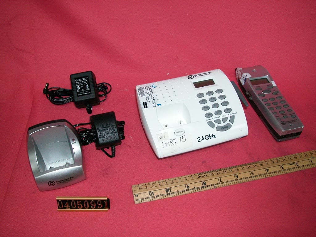
Jul 25, 20042.4GHz 40 Channel Cordless Phone w/ CID
Equipment Class
DXT - Part 15 Low Power Transceiver, Rx Verified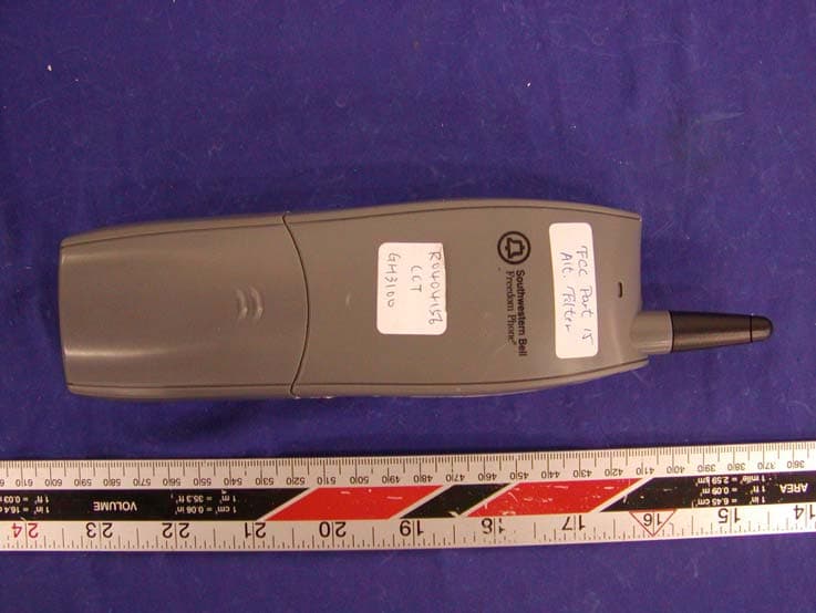
LBBGH3100H
May 06, 2004Cordless Phone
Equipment Class
DXX - Part 15 Low Power Communication Device Transmitter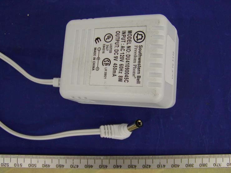
LBBGH3100
May 06, 2004Cordless Phone
Equipment Class
DXX - Part 15 Low Power Communication Device Transmitter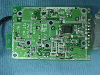
LBBGH3062
Apr 25, 20042.4 GHz Cordless Phone with Radio
Equipment Class
DXX - Part 15 Low Power Communication Device Transmitter
LBBGH4100
Apr 05, 20042.4GHz FHSS Cordless Phone w/ CID
Equipment Class
DSS - Part 15 Spread Spectrum Transmitter