LBBFRS216FRS+GMRS
Continental Conair Limited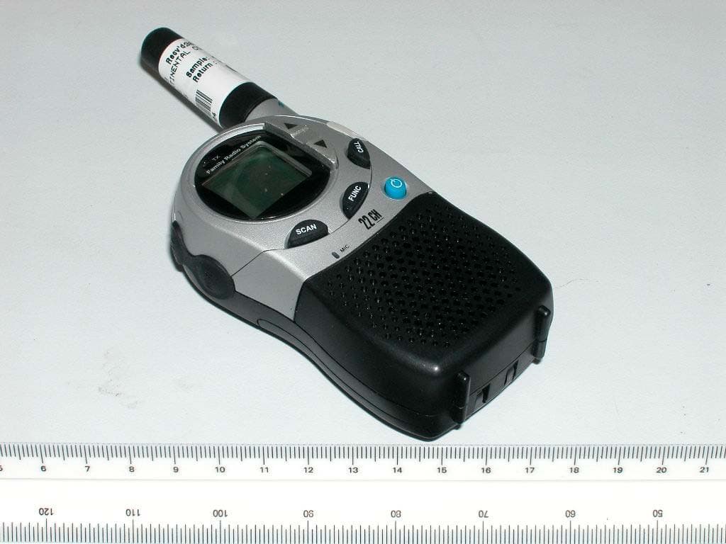
Click to zoom
Application Details
- Equipment Class
- FRF - Part 95 Family Radio Face Held Transmitter
- Date of Grant
- Nov 10, 2003
- Application Purpose
- Original Equipment
- Date of Application
- Nov 10, 2003
- Equipment Note
- FRS+GMRS
- Frequency Range
- 467.56250000 - 467.71250000
- Company
- Continental Conair Limited
- Country
- Hong Kong
Documents & Files
Document Text
Text extracted from the exhibit documents filed with the FCC. Open a document above to read the original.
Users Manual
2 3 1 UHF FM TRANSCEIVER (Family Radio Service) FRS310HT IB-4833 Printed in China IMPORTANT SERVICE INFORMATION SAVE THESE INSTRUCTIONS BLISTER PACK CONTENTS Read this manual before attempting to set up or use this instrument. It contains important information regarding safe installation and use. Keep this manual for future reference. Also save the carton, packing and proof of purchase to simplify and accelerate any needed action. FRS316-Two (2) Two-Way Radios * Attached to the units at the time of packing User-Removable Belt Clips* Two (2) Rechargeable Battery Packs FRS Charger with AC/DC Adaptor User's Manual FCC NOTICE FRS PRODUCT DESCRIPTION The FCC requires that you be advised of certain requirements involving the use of this device. This equipment has been tested and found to comply with the limits for a Class B digital device, pursuant to Part 15 of FCC Rules. These limits are designed to provide reasonable protection against harmful interference in residential installation. This device uses and can generate radio frequency energy. If not installed and used in accordance with the instructions, it may cause harmful interference to radio communications. However, there is no guarantee that the interference will not occur in a particular installation. If this equipment does cause harmful interference to radio or television reception (which can be determined by turning the unit off and on), the user is encouraged to correct the interference by one or more of the following measures: Reorient or relocate the receiving antenna. Increase the separation between the equipment and receiver. Connect the equipment to an outlet on a circuit different from that to which the receiver is connected. Consult the dealer or an experienced radio/TV technician for help. FCC WARNING: This equipment generates or uses radio frequency energy. Adjustment to this unit or replacement of any transmitter component (crystal, semiconductor, etc.) to this unit that could result in violation of the rules. FCC INFORMATION: This device complies with part 15 of the FCC Rules. Operation is subject to the following two conditions:(1) This device may not cause harmful interference, and (2) this device must accept any interference received, including interference that may cause undesired operation. Privacy of communications SAFETY INFORMATION: Your wireless hand-held portable transceiver contains a low power transmitter. When the PUSH TO TALK (PTT) button is pushed it sends out radio frequency (RF) signals. The device is authorized to operate at a duty factor not to exceed 50%. In August 1996, the Federal Communications Commissions (FCC) adopted RF exposure guidelines with safety levels for hand-held wireless devices. may not be ensured when using this equipment. CAUTION: To maintain compliance with the FCC's RF exposure guidelines hold the transmitter and ANTENNA at least 1 inch (2.5 cm) from your face and speak in a normal voice, with the ANTENNA pointed up and away from the face. If you wear the handset on your body while using the headset accessory, use only the supplied belt clip for this product and when transmitting, take it out of the belt to ensure that the ANTENNA is at least 1 inch (2.5 cm) from your body. Use only the supplied ANTENNA. Unauthorized antennas, modifications, or attachments could damage the transmitter and may violate FCC regulations. NOTE: The maximum transmission range will vary depending on terrain and environment. Range will be greater in open fields, while the range is shorter within and around buildings or large structures. FRS316 FRS316 FRS1FRS 2 BATT 1BATT 2 by The FRS316 is compatible with other brands utilizing the same frequency band (operating in the frequency range from 462.5625MHz to 462.7250MHz). Please read this user's manual thoroughly to get the most out of your FRS316 two-way radio. The FRS316 is a 22-channel UHF two-way radio, featuring a multi-functional LCD panel (which indicates the current channel and various radio status icons). Other features also include electronic volume control and battery save circuitry. The FRS/GMRS is the newest generation in personal two-way communications. The FRS/GMRS operates in a licensed radio band (FCC license is needed for its operation), on any of the GMRS channels. The FRS316 is a lightweight, compact two-way radio that can be used up to about two miles with family or friends at parks, shopping malls, sporting events, concerts--any indoor or outdoor activity! S C A N F U N C C A L L CH 22 MIC FCC Licensing Information Insert S C A N F U N C C A L L CH 22 MIC INSTALLATION Removing the Belt Clip Installing the Belt Clip 1.) BELT CLIP LATCH FIGURE 1 (REAR VIEW) FIGURE 2 (REAR VIEW) BELT CLIP SLOT 2.) BELT CLIP 1. Pull the BELT CLIP LATCH (1) away from the unit. 2. While pulling the BELT CLIP LATCH (1), push up on the BELT CLIP (2) to remove it from the unit, as shown in Figure 1. 1. Slide the BELT CLIP into the BELT CLIP SLOT as shown in Figure 2. BATT 1BATT 1BATT 2BATT 2 FRS1FRS1FRS 2FRS 2 MAXIMUM RANGE PERFORMANCEMAXIMUM RANGE PERFORMANCE SAFETY INSTRUCTIONS FOR BATTERIES CONTAINS NICKEL-CADMIUM BATTERY. BATTERY MUST BE RECYCLED OR DISPOSED OF PROPERLY. CAUTION: To reduce the risk of fire or personal injury, read and follow these instructions.: 1. Use only a CONAIR approved battery pack in FRS316. a. GP35AAAK4BX 4.8V 350mA GPI International Ltd. or b. JB35AAANC4BC 4.8V 350mA JB Energy (HK) Ltd. 2. Do not dispose of the battery in a fire, as it may explode. Check with local codes for possible special disposal instructions. 3. Do not open or mutilate the battery. Released electrolyte is corrosive and may cause damage to the eyes and skin. It may be toxic if swallowed. 4. Exercise care in handling batteries in order not to short the battery with conducting materials such as rings, bracelets and keys. The battery or conduction material may overheat and cause burns. 5. Charge the battery (ies) provided with or identified for use with this product…
Text truncated - open the document above for the full version.
Block Diagram
FRS316BD.sch-1 - Mon Jun 23 11:38:33 2003
External Photos
Test Setup FCCID : LBBFRS216 External Photo -front External Photo – rear
ID Label/Location Info
MODEL: FRS216 FCC ID: LBBFRS216 HT0603-V01-000001 Date Code label FCC label Lens sticker label QC Pass label 35.7mm 14.7mm 22mm 22mm6mm SC MODEL: FRS216 FCC ID: LBBFRS216 HT0603-V01-000001 Sequential Number Version Number Year Month Company Initial 34mm 7mm SC
Internal Photos
Test Setup FCC ID : LBBFRS216 Internal Photo – 1 Internal Photo - 2 Test Setup FCC ID : LBBFRS216 Internal Photo – 3 Internal Photo – 4 Test Setup FCC ID : LBBFRS216 Internal Photo – 5
Operational Description
LIONDA TECHNOLOGY COMPANY LIMITED Lionda Research and Development Center FRS316 desc Page 1 5/6/03 CIRCUIT DESCRIPTION Model: FRS316 a. Receiver Section Radio Frequency signal received by the antenna (ANT1), passing through the Low Pass Filter (L2-L3, C30-C31). The RF signal is then amplified by Low Noise Amplifier Q2 and passes through a Band Pass Filter FL1 (465MHz). The filtered signal within the range of 462 MHz – 467 MHz is then mixed with the first local oscillator signal from the Voltage Controlled Oscillator (VCO) circuit (Q9, Q20-Q21, D7, L18) through Q11, a portion of VCO signal is then feedback to the PLL IC (IC5) for phase comparison generating a stable RX Frequency, the output signal is filtered by FL2 (10.7 MHz) which is the first Intermediate Frequency (IF) and is then amplified by Q14. The IF signal is fed to the discriminator IC (IC2) pin 16 which is then mixed with the second local oscillator supplied by crystal X2 (21.25 MHz) to produced and reduced second IF signal. Demodulated signal is recovered through correct adjustment of IF coil (L13) and the internal discriminator circuit of IC2. The recovered Audio signal is outputted at pin 9 of IC2 and then processed through filtering done by U3D circuit, the fully recovered audio signal is then further amplified by Power Amplifier U3A. An audible sound is therefore produce by the speaker SPK1, which can be varied from minimum to maximum through the key function (up/down) and process by the CPU IC6. b. Transmitter Section PTT switch (SW100) when pushed triggers the Transmitter Circuit “ON”, the voice signal generates by the surrounding noise passes through the Microphone MIC1 where mechanical to electrical transformation occurs, the electrical transformed signal is then filtered by a Band Pass Filter U3A, D, and C. The output signal is Modulated by a modulator circuit with a varactor diode D7 and L18. The external components from Q9-Q11 form a VCO Circuit, which generates the required oscillating frequency for transmission; a portion of this signal is feedback to the PLL IC2 pin 14 for phase comparison in order to produce a stabilized TX frequency. The modulated signal is then amplified by a Cascaded Amplifier Circuit Q7 and Q8 and again amplified by Q5 and Q6 to produce a sufficient Radio Frequency signal emitted by the Antenna (ANT1). c. Call Transmission By pushing the CALL key, a signal is detected by the CPU (IC6), a CALL data is then produced by the CPU. This data passes through the Band Pass Filter U1C and modulated by the varactor diode D4 and L1. The signal follows it’s conventional transmission section path through the antenna. d. Battery Low Detection Battery Low Detection is controlled by the IC6 as detected on the LCD1, however a voltage divider circuit R50 and R51 serve as the stabilize reference voltage for the IC6 to process its detection. LIONDA TECHNOLOGY COMPANY LIMITED Lionda Research and Development Center FRS316 desc Page 2 5/6/03 e. Squelch Detection Supported by the linear IC circuit (IC2), a variable resistor VR1 sets the level of detection and Diode D11 acts as a comparator circuit interface with the CPU IC6. f. Power Supply Supply voltage of 6 Volts dc is needed to power “ON” the whole circuitry, by four (4) batteries “AAA” size. FREQUENCY CHART CHANNEL FREQUENCY (MHz) CHANNEL FREQUENCY (MHz) 1 462.5625 12 467.6625 2 462.5875 13 467.6875 3 462.6125 14 467.7125 4 462.6375 15 462.5500 5 462.6625 16 462.5750 6 462.6875 17 462.6000 7 462.7125 18 462.6250 8 467.5625 19 462.6500 9 467.5875 20 462.6750 10 467.6125 21 462.7000 11 467.6375 22 462.7250
Parts List/Tune Up Info
TUNE-UP PROCEDURE Model FRS216 Page 1 8/12/03 FRS216/FRS316 1. TRANSMITTING 1.1 TX VCO ADJUSTMENT a) Connect the DC voltmeter to the test point 1 (TP1). b) Press the PTT Button. c) Adjust L18. d) Specification: 0.9Vdc +/- 0.3 V @ CH 1 1.2 FREQUENCY ADJUSTMENT a) Connect the frequency counter to ANT point. b) Adjust CV1. c) Specification: Tx Frequency +/- 200Hz 1.3 TX POWER CHECK a) Connect the RF level meter to the ANT point (RF impedance: 50Ω) b) Press the PTT button. c) Check the TX Power d) Specification: CH4: 0.21Watt (ERP); CH11: 0.09Watt (ERP) 1.4 MAX. DEVIATION ADJUSTMENT a) Connect the deviation meter to the ANT point. b) Apply the audio signal 1KHz, 4mVrms to the test point 7 (TP7 - MIC input) c) Observe the clipped signal on the scope. d) Adjust SVR1. e) Specification: 2.5KHz Dev +/- 0.15KHz 1.5 MODULATION SENSITIVITY ADJUSTMENT a) Connect the deviation meter to the ANT point. b) Apply the audio signal 1KHz, 8mVrms to the test point (TP7 - MIC input). c) Adjust SVR1. d) Specification: 0.9-1.0KHz Dev 1.6 CALL DATA MODULATION SENSITIVITY CHECK a) Press the Call Button and observe the deviation meter to check the deviation. b) Specification: 1.8KHz +/- 0.5KHz 2. RECEIVING 2.1 RX VCO CHECK a) Connect the DC voltmeter to test point 1 (TP1). b) Check the DC voltage. c) Specification: 0.9Vdc +/- 0.6V @ CH 1 TUNE-UP PROCEDURE Model FRS216 Page 2 8/12/03 FRS216/FRS316 2.2 QUAD COIL ADJUSTMENT a) Connect the DC voltmeter to the test point 3 (TP3). b) Adjust the IFT1. c) Specification: 1.5Vdc +/- 0.2V 2.3 SENSITIVITY CHECK a) Connect the Sinnader meter to test point 5 (TP5). b) Reduce the RF output level of signal generator to get the 12dB of Sinnader. c) Specification: <-112dBm 2.4 SQUELCH THRESHOLD POINT ADJUSTMENT a) Connect the DC voltmeter to test point 16. b) Same setup as the Sensitivity Check. c) Adjust the SVR1 to get the DC changing point. d) Specification: 7dB +/- 1dB 2.5 SPEAKER OUTPUT LEVEL CHECK a) Connect the Audio level meter to test point 5 (TP5). b) Connect the 8Ω load to test point 5 (TP5). c) Press the volume button till its maximum level. d) Adjust the modulation deviation of RF signal generator. e) Check the clipping start deviation & level. f) Specification: Clipping start deviation = >0.6KHz Level = -2 +/- 4 dBm NOTE: 1. Press PTT button continuously when checking TRANSMITTING parameters. 2. Press the Monitor button to disable the RX power saving when the RX is not stable. 3. OTHER PARAMETER CHECKING 3.1 LOW BATTERY DETECT VOLTAGE CHECK a) Change the voltage until the Battery icon is flashing on the LCD. b) Check the voltage. c) Specification: 4.2Vdc +/- 0.3V
Parts List/Tune Up Info
••••: 2003-08-08•••• •••••5 ••••451065000300 IC_LI KA324/KIA324/LM324(SOP) 1.000451065000400 IC _ LI TB31202FN(SOP) 1.000 220471270280 CAP _ C _ C.H.D. B470PF/K/(0402) 2.000 220820260170 CAP _ C _ CHIP 82PF/J(CH)/0402 2.000 220102270280 CAP _ C _ C.H.D. B0.001uF/K/(0402) 12.000 220103280330 CAP _ C _ C.H.D. F0.01uF/M/0402 13.000 220223280330 CAP _ C _ C.H.D. F0.022uF/M/0402 6.000 220682280280 CAP _ C _ C.H.D. B0.0068uF/M/0402 1.000 220473290330 CAP _ C _ C.H.D. F0.047uF/Z/0402 5.000 220104290330 CAP _ C _ C.H.D. F0.1uF/Z/0402/Y5V 20.000 220105292330 CAP _ C _ C.H.D. F 1uF/Z(0805)Y:YF153L 11.000 220224292330 CAP _ C _ C.H.D.F0.22uF/Z(0805)Y:YF153L 1.000 790981910010 PCB _ FRS 316 REV:01 1.000 304027010100 CHIP COIL SQUARE 27nH/K(0603) 1.000453041000101 IC _ MOS VOLTAGE REGULATORTAR5S40(SOT-89) 1.000 100104030000 RES _ (0402)-16 100 KOHM 12.000 220474292330 CAP _ C _ C.H.D.F0.47uF/Z(0805)Y:YF153L 2.000 321203205010 CHIP SPRING COIL D1.2X0.32X5T 1.000220106073240 CAP _ C _ MLCC 10uF/(1206)/10V(MURATA) 3.000 100000132000 RES _ (0805)-10 0 OHM 1.000 100563030000 RES _ (0402)-16 56 KOHM 2.000 220103271280 CAP _ C _ C.H.D. B0.01uF/K(0603)X:X7R282L 1.000 220101261170 CAP _ C _ CHIP 100PF/J(CH)(0603)A:COG150L 1.000 220120260170 CAP _ C CHIP 12PF/J/(CH)/(0402) 1.000 451065000600 IC _ LI KA386/LM386(SOP-8) 1.000 452067000200 IC _ COM TA31180FN (SSOP-24) 1.000 411040000000 TR _ SS KST2907TF/KTN2907S/AS /MMBT2907LT1(SOT-23) 5.000 410240000002 TR _ SS MMBT3904LT1(SOT-23) 4.000 416141000001 TR _ RF POWER BFQ540(SOT-89) 1.000 412140000200 TR _ RF KSC2223Y (SOT-23) 1.000 412240000200 TR _ RF 2SC4901 (SOT-23) HFE:120-250 6.000 432461400000 LED CHIP GREEN ELT-0805GC 1.000405135000000 DIODE _ SW KDS114(URP) 4.000 405231000000 DIODE _ SW LL4148/MM4148 MELF 2.000 402035000001 DIODE VAR BB149A (URP) 1.000100000030000 RES _ (0402)-16 0 OHM 7.000 100100030000 RES _ (0402)-16 10 OHM 8.000 100101030000 RES _ (0402)-16 100 OHM 3.000 100102030000 RES _ (0402)-16 1 KOHM 9.000 100103030000 RES _ (0402)-16 10 KOHM 7.000 100122030000 RES _ (0402)-16 1.2 KOHM 1.000 100153030000 RES _ (0402)-16 15 KOHM 2.000 100154030000 RES _ (0402)-16 150 KOHM 1.000 100155030000 RES _ (0402)-16 1.5 MOHM 1.000 100182030000 RES _ (0402)-16 1.8 KOHM 2.000 100183030000 RES _ (0402)-16 18 KOHM 2.000 100222030000 RES _ (0402)-16 2.2 KOHM 9.000 100223030000 RES _ (0402)-16 22 KOHM 14.000 •••••1U3IC5C19,C88C128,C133C24,C29,C33,C34,C53,C67,C102,C119,C140,C145,C147,C148C74,C82,C89,C91,C98,C104,C110,C113,C45,C141,C144,C151,R186C47,C50,C52,C68,C71,C105R13C40,C70,C75,C76,C79C13,C16,C25,C26,C36,C69,C99,C106,C125,C126,C41,C51,C54,C78,C8 6 C6,C9,C27,C90,C136,C138,C146,C77,C217,C231,C229C152PCB _ FRS L18IC8R107,R108,R109,R11,R52,R56,R67,R73,R84,R97,R204,R205C18,C35L9C228,C111,C230LED1C12,R61C103C107C48IC1IC2Q1,Q5,Q6,Q7,Q13Q4,Q9,Q15,Q21Q24Q14Q2,Q11,Q18,Q19,Q20,Q26 LED3D2,D3,D4,D5R39,D9D8R63,R137,C176,C21,R23,R312,C58R10,R18,R53,R69,R123,R126,R151,R152R38,R43,R135R2,R14,R75,R105,R140,R141,R142,R147,R309R54,R101,R134,R139,R145,R230,R310R81R27,R182R58R185R12,R71R200,R203R29,R42,R76,R116,R117,R122,R131,R138,R153R30,R40,R44,R46,R47,R48,R49,R50,R51,R66,R115,R127,R150,R242 ••••: 2003-08-08•••• •••••5 •••• 501327606000 XTAL_32.768KHz D3X8 1.000501212511010 XTAL _ 21.250MHz (18PF) HC-49S(3.6mm) +/-3PPM(-10~+65•) RALTR 1.000 503021321000 CRYSTAL FILTERS 21.3MHz(ft21.3)3dB BANDWIDTH + 2.000601212110000 SWITCH _ FUNCTION IT-1207-3180 2.000 751100010100 SHIELD COVER FRS99150 (TINNING) 1.000092000906022 DICE _ FRS 216 U8567-LD014H 4EA9 1.000 600421010000 EARPHONE JACK(2.6mm) ST-020SMT(STEREO) FOR 39230 1.000742821000220 SPONGE _ PLATE 5X10X1mm (WHITE) 1.000 745000010030 FIBRE SHEET 9.5X9.5X0.3mm(SINGLE TYPE) 1.000200100421000 CAP _ E _ MINI 10uF/25V(D4XL7) 2.000 200101221000 CAP _ E _ MINI 100uF/10V(D5XL7) 1.000 280100002030 CAP _ C _ TRIMMER 10PF (SMT) 1.000 430410000100 LED RED 3142D 1.000200101121012 CAP _ E _ MINI100uF/6.3V(D4XL7)KSC 2.000 200220321002 CAP _ E _ MINI 22uF/16V(D4XL7)KSC 1.000 751120004100 COPPER PLATE 9X10X0.2t(SINGLE TAPE) FOR FRS1022 1.000PCBA _ FRS 216 REV:02
Test Report
Modulation Limiting Characteristic 0.000.501.001.502.002.50 47 57 67 77 87 97 107 117 127 137 Modulation Input (dBSPL) Frequency Deviation (kHz) 500Hz1000Hz2500Hz3125Hz
Test Report
• The test results reported in this report shall refer only to the sample actually tested and shall not refer or be deemed a refer to bulk from which such a sample may be said to have been obtained. • This report shall not be reproduced except in full without prior authorization from Intertek Testing Services Hong Kong Limited • For Terms And Conditions of the services, it can be provided upon request. • The evaluation data of the report will be kept for 3 years from the date of issuance. Intertek Testing Services Hong Kong Ltd. 2/F., Garment Centre, 576 Castle Peak Road, Kowloon, Hong Kong. Tel: (852) 2173 8888 Fax: (852) 2371 0521 Website: www.hk.intertek-etlsemko.com Continental Conair Ltd. Application For Certification (FCC ID: LBBFRS216) September 11, 2003 0305983 DL/ Sandy September 11, 2003 INTERTEK TESTING SERVICES FCC ID: LBBFRS216 i SUMMARY OF CONTENTS LIST OF EXHIBITS EXHIBIT 1: General Description EXHIBIT 2: System Test Configuration EXHIBIT 3: RF Power Output EXHIBIT 4: Modulation Characteristics EXHIBIT 5: Occupied Bandwidth EXHIBIT 6: Spurious Emission EXHIBIT 7: Frequency Stability EXHIBIT 8: Technical Specifications EXHIBIT 9: Product Labelling EXHIBIT 10: Photographs EXHIBIT 11: Instruction Manual EXHIBIT 12: Tune Up Procedure EXHIBIT 13: Part List EXHIBIT 14: Input Current EXHIBIT 15: RF Exposure Info INTERTEK TESTING SERVICES FCC ID: LBBFRS216 ii MEASUREMENT/TECHNICAL REPORT Application : Continental Conair Ltd. Trade Name/Model No : CONAIR FRS216SLV CONAIR FRS316SLV Date : September 11, 2003 This report concerns (check one:)Original Grant X Class II Change Equipment Type: GMRS + FRS Deferred grant requested per 47 CFR 0.457(d)(1)(ii)? Yes No X If yes, defer until: date Company Name agrees to notify the Commission by: date of the intended date of announcement of the product so that the grant can be issued on that date. Report prepared by: Derek Leung Intertek Testing Services 2/F., Garment Centre, 576 Castle Peak Road, Kowloon, Hong Kong. Phone: 852-2173-8504 Fax: 852-2371-0521 INTERTEK TESTING SERVICES FCC ID: LBBFRS216 iii Table of Contents 1.0 General Description............................................................................................ 2 1.1 Product Description ......................................................................................... 2 1.2 Related Submittal(s) Grants ........................................................................... 3 1.3 Test Methodology........................................................................................... 3 1.4 Test Facility .................................................................................................... 3 2.0 System Test Configuration................................................................................. 5 2.1 Justification...................................................................................................... 5 2.2 EUT Exercising Software................................................................................ 6 2.3 Special Accessories........................................................................................ 6 2.4 Measurement Uncertainty............................................................................... 6 2.5 Equipment Modification ................................................................................... 6 3.0 RF Output Power (Section 95.639(d))................................................................. 8 4.0 Modulation Characteristics (Section 95.637(a))............................................... 12 4.1 Modulation Frequiency Response .................................................................. 13 4.2 Modulation Limiting Characteristic.................................................................. 15 4.3 Audio Low Pass Filter Response .................................................................. 17 5.0 Occupied Bandwidth (Section 95.633(c)) ........................................................ 19 6.0 Spurious Emission (Section 95.635(b)) ........................................................... 21 6.1 Field Strength of Spurious Radiation.............................................................. 22 7.0 Frequency Stability (Section 95.627)............................................................... 28 7.1 Frequency Tolerance..................................................................................... 29 7.2 Temperature Extreme Condition..................................................................... 31 7.3 Voltage Extreme Condition............................................................................. 34 8.0 Technical Specifications.................................................................................. 37 9.0 Product Labelling.............................................................................................. 41 10.0 Equipment Photographs................................................................................. 44 11.0 Instruction Manual.......................................................................................... 46 12.0 Tune Up Procedure......................................................................................... 48 13.0 Part List........................................................................................................... 50 14.0 Input Current................................................................................................... 52 15.0 RF Exposure Info............................................................................................ 54 INTERTEK TESTING SERVICES FCC ID: LBBFRS216 iv List of attached file Exhibit type File Description Filename Operation Description Technical Description descri.pdf Test Report Bandwidth Plot bw.pdf Test Report Modulation Frequency Response mfr.pdf Test Report Modulation Limit Characteristic mlc.pdf Test Report Spurious Emission spurious.pdf Block Diagram Block Diagram block.pdf Schematics Circuit Diagram circuit.pdf ID Label…
Text truncated - open the document above for the full version.
Test Report
Audio Low Pass Filter Response -70.0-60.0-50.0-40.0-30.0-20.0-10.0 0.0 10.0 1 10 100 Frequency (kHz) dB relative to 1 kHz LPF ResponseTIA/EIA-603
Test Setup Photos
Test Setup FCCID : LBBFRS216 Radiated -front Radiated - rear
Contact Information
Applicant
David Ng(Manager, Consumer Electronics)
852 2751 4688Fax: 852 2751 8920
Technical Contact
Intertek Testing Services Hong Kong Ltd.Derek Leung
[email protected]852-2173-8504
2/F., Garment Centre, · Kowloon, · Hong Kong
Non-Technical Contact
Intertek Testing Services Hong KongDerek Leung
[email protected]852-2173-8504
Test Firm
Intertek Testing Services Hong KongBilly Chow
Technical Specifications
| # | Rule Parts | Frequency Range | Power Output | Emission | Tolerance |
|---|---|---|---|---|---|
| 2 | 95B | 467.5625 MHz - 467.7125 MHz | 90.00 mW | 8K00F3E | 2.5 ppm |
Other Applications from Continental Conair Limited
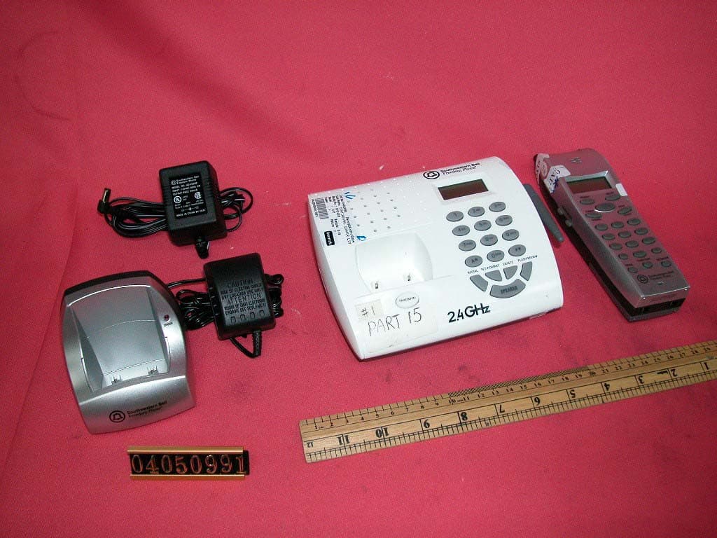
LBBGH3128AT
Jul 25, 20042.4GHz 40 Channel Cordless Phone w/ CID
Equipment Class
DXT - Part 15 Low Power Transceiver, Rx Verified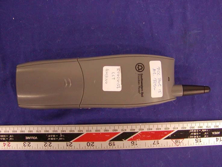
LBBGH3100H
May 06, 2004Cordless Phone
Equipment Class
DXX - Part 15 Low Power Communication Device Transmitter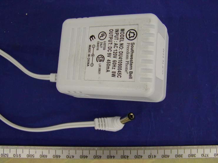
LBBGH3100
May 06, 2004Cordless Phone
Equipment Class
DXX - Part 15 Low Power Communication Device Transmitter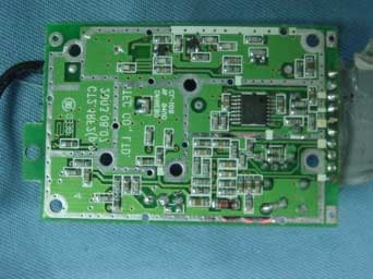
LBBGH3062
Apr 25, 20042.4 GHz Cordless Phone with Radio
Equipment Class
DXX - Part 15 Low Power Communication Device Transmitter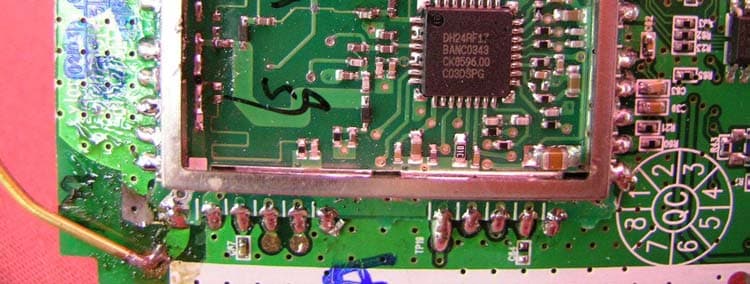
LBBGH4100
Apr 05, 20042.4GHz FHSS Cordless Phone w/ CID
Equipment Class
DSS - Part 15 Spread Spectrum Transmitter