LBBGH3012AT2.4GHz 40 Channel Analog Modulation Cordless Phone
Continental Conair Limited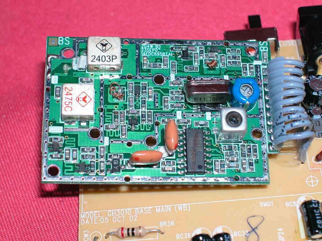
Click to zoom
Application Details
- Equipment Class
- DXT - Part 15 Low Power Transceiver, Rx Verified
- Date of Grant
- Jun 23, 2003
- Application Purpose
- Original Equipment
- Date of Application
- Jun 22, 2003
- Equipment Note
- 2.4GHz 40 Channel Analog Modulation Cordless Phone
- Frequency Range
- 2474.00000000 - 2475.95000000
- Company
- Continental Conair Limited
- Country
- Hong Kong
Documents & Files
Document Text
Text extracted from the exhibit documents filed with the FCC. Open a document above to read the original.
ID Label/Location Info
3012NB Rev.1 03/20/2003 P/T TEL LINE DC9V 200mA DC9V200mA USE ONLY WITH CLASS 2 POWER SOURCE USEONLYWITH CLASS 2POWERSOURCE V01A AT 0303 S/N:CXXXXXX US ® L I S T E D L I S T E D 70255 PRIVACY OF COMMUNICATIONS MAY NOT BE ENSURED WHEN USING THIS PHONE. FCC ID : LBBGH3012AT THIS DEVICE COMPLIES WITH PART 15 OF THE FCC RULES. OPERATION IS SUBJECT TO THE FOLLOWING TWO CONDITIONS: (1) THIS DEVICE MAY NOT CAUSE HARMFUL INTERFERENCE, AND (2) THIS DEVICE MUST ACCEPT ANY INTERFERENCE RECEIVED, INCLUDING INTERFERENCE THAT MAY CAUSE UNDESIRED OPERATION. CONFORMS TO ANSI/UL STD. 1950 Southwestern Bell ® Complies with 47 CFR Part 68 requirements REGISTRATION NUMBER: US: SBFW909BGH3010AT USOC JACK: RJ11CREN: 0.9B HAC MADE IN CHINA MANUFACTURED TO BELL SPECIFICATIONS MODEL No. GH3012AT LICENSED UNDER UNITED STATES PATENT NO. 5,263,084 FCC ID: LBBGH3012AT Model number GH3012AT
Internal Photos
Internal photos FCC ID: LBBGH3012AT Base assembly (View 1) Base assembly (View 2) Internal photos FCC ID: LBBGH3012AT Base Main PCB comp side (View 1) Base Main PCB comp side (View 2) Internal photos FCC ID: LBBGH3012AT Base Main PCB solder side Base Oscillator PCB comp side Internal photos FCC ID: LBBGH3012AT Base Oscillator PCB solder side Handset assembly Internal photos FCC ID: LBBGH3012AT Handset Main PCB comp side Handset Main PCB solder side Internal photos FCC ID: LBBGH3012AT Handset Main PCB display front side Handset Main PCB display rear side Internal photos FCC ID: LBBGH3012AT Handset keypad front side Handset keypad side rear side (View 1) Internal photos FCC ID: LBBGH3012AT Handset keypad side rear side (View 2) Handset Oscillator PCB comp side Internal photos FCC ID: LBBGH3012AT Handset Oscillator PCB solder side
Operational Description
GH3012 Circuit Description 1. Introduction The model 3012 is a 40 channel (2.40255-2.47595GHz ) Caller ID cordless telephone. The whole unit is divided into two main parts as follow : a. A remote Handset. b. A Base unit. 2. Functional Blocks of the Remote Handset 2.1 Keyboard matrix and function LED 2.2 LCD 2.3 MCU and MCU interface 2.4 Antenna and RF module 2.5 Compander 2.6 Data shaper 2.7 Charge detector 2.8 Low battery detector 2.9 Buzzer amplifier 3. Circuit Block Description 3.1 Keyboard matrix and function LED Pin 46 to pin51, pin 54 to pin 58 of the MCU:U1 NT93423 form a keyboard, and the new call LED is controlled by the pin 73 of the MCU. 3.2 LCD LCD1 is controlled by the MCU: U1 NT93423 pin 1 to pin 32, pin 103 to pin 128. 3.3 MCU and MCU interface The handset and the base is link up by the pins(45,78 in HS and 43,78 in Base). Besides, the PLL of the RF Module is controlled by the pins 39 to pin 41 of the MCU. 3.4 Antenna and RF module ANT is the common point for transmitting and receiving through antenna. MD1 is a RF module which consists of Filter, Power amplifier, Mixer & IF, RXVCO, TXVCO, VCC & TXVCC control, Synthesizer and DEMO Audio Output circuits. RF module circuit can be described as followings: 3.4.1 Power Supply 3.4.2 PLL and MCU Interface 3.4.3 RF Transmitter 3.4.4 RF Receiver 3.4.5 Audio Detector 3.4.1 Power Supply The RF transmitter receives power from TXVCC. TXVCC is enabled only during TALK mode.The RF receiver receives power from RXVCC. RXVCC is enabled only during TALK or stand-by mode when wake up. 3.4.2 PLL and MCU Interface The frequencies of the RF transmitter and RF local oscillator are controlled by PLL IC U1. The MCU transmit PLL data through DATA, CLK and CE signal lines. The basic clock frequency of the PLL is derived from an 11.15MHz crystal inside the RF module. The local frequencies to TX and RX are generated and locked at 825MHz and 798MHz respectively. 3.4.3 RF Transmitter The RF transmitter oscillator frequency 825MHz is controlled by the PLL through Vt. The PLL samples the RF frequency through fin. The audio input signal AFIN is fed to this RF oscillator through the FM modulator. Fundamental frequency 825MHz is multiplied to 2475MHz and bypass through band pass filter formed by Q7, ML5, C5, C37 and ML4. The filtered 2475MHz is then injected into TX power amplifier Q6 and related passive components. The enlarged 2475MHz rf signal is then input into the 2475MHz TX_FILTER, DF1. The transmitted rf signal is then injected into the ANTENNA and radiated out into air. 3.4.4 RF Receiver Received rf signal is collected from ANTENNA and passed through 2403MHz filter DF2. The filtered 2403MHz rf signal will then be injected into the LNA Q3 and be enlarged. The amplified 2403MHz signal is then input into the MIXER which is formed by Q4 and related passive components. Q2 and VD2 with related resistors and capacitors network form the RXVCO which is fed and locked by the PLL U1. The fundamental 798MHz frequency is multiplied to 2393MHz and bypass the BPF formed by C28, ML11, C26, C25, ML13 and C 50 to the receiver mixer. The receiver local oscillator frequency is controlled by the PLL through Vt. The PLL samples the local oscillator RF frequency through fin. The mixer collects the input from LNA and 2393MHz signal from BPF and then output the IF 10.7MHz into Q5. 3.4.5 Audio Detector Amplified IF from Q5 is passed into 10.7MHz filter CF1,amplifier Q8 , 10.7MHz filter CF3 and then injected into the IF demodulated IC U4. Detected audio will then be recovered and output at the AFOUT pin of the RF module. 3.5 Compander A compander U1 is used for improving the S/N of the transmit and receive audio signal. 3.6 Data shaper The information which sending from base unit, is recovered by the amplifier Q1 and MQ4,MQ5. 3.7 Charge detector MD3 to MD6, MZD1, MR23,MC9 and MR22 form a charge detector to direct the charging signal to the MCU pin 34. 3.8 Low battery detector A battery low detector is built-in by the Q2, R5 to R7 and D2 which detects the battery dropping and sends a signal to pin 36 of MCU. 3.9 Buzzer amplifier Q4 is a buzzer amplifier driven directly by the MCU pin 61. 4. Functional Blocks of the Base unit 4.1 Power supply 4.2 MCU and MCU interface 4.3 Calling line identifier 4.4 Antenna and RF module 4.5 Compander 4.6 Data shaper 4.7 Charge detector 4.8 Line audio interface 4.9 Ring detector 4.10 Led function board 4.11 Carrier detector 5. Circuit Block Description 5.1 Power supply BU1 7805 regulate the input DC 9V to 5V which provides power to every part of the circuit. 5.2 MCU and MCU interface The heart of the base is MCU BMU1: NT93423A that communicates with the PLL of BMD1 through pins 39,40 and 41. Transmitter is controlled by the signal TX_DC which output from MCU via pin 53. MCU pin 95 is for generating DTMF signal. The communication between Handset and Base is via the pin 43 and pin 76 through the RF link. 5.3 Calling line identifier MCU pin 87 to pin 88, when receiving caller ID data, MCU controls the LCD to display the correct information. 5.4 Antenna and RF modulator ANT is antenna transmit and receive signal. BMD1 is a RF modulator which consist of Filter, Power amplifier, Mixer & IF, RXVCO, TXVCO, VCC & TXVCC control, Synthesizer and DEMO Audio Output circuits. The block diagram of RF Module is as shown below. It is made up of the following parts: 5.4.1 Power Supply 5.4.2 PLL and MCU Interface 5.4.3 RF Transmitter 5.4.4 RF Receiver 5.4.5 Audio Detector 5.4.1 Power Supply The RF transmitter receives power from TXVCC. TXVCC is enabled only during TALK mode or Ring mode. The RF receiver receives power from RXVCC. RXVCC is enabled when BASE plug in DC adapter. 5.4.2 PLL and MCU Interface The frequencies of the RF transmitter and RF local oscillator are controlled by PLL IC U1. The MCU transmit PLL data through DATA, CLK and CE signal lines. The basic clock frequency of the PLL is derived from an 11.15MHz crystal inside the RF module. The local freque…
Text truncated - open the document above for the full version.
Test Report
• The test results reported in this report shall refer only to the sample actually tested and shall not refer or be deemed to refer to bulk from which such a sample may be said to have been obtained. • This report shall not be reproduced except in full without prior authorization form Intertek Testing Services Limited FCC ID: LBBGH3012AT Intertek Testing Services Hong Kong Ltd. 2/F., Garment Centre, 576 Castle Peak Road, Kowloon, Hong Kong. Tel: (852) 2173 8888 Fax: (852) 2741 1693 Continental Conair Limited Application For Certification 2.4GHz 40 Channel Analog Modulation Cordless Phone with Caller ID (FCC ID: LBBGH3012AT) WO# 03032031 TL/Ann Choy April 8, 2003 INTERTEK TESTING SERVICES FCC ID: LBBGH3012AT i LIST OF EXHIBITS INTRODUCTION EXHIBIT 1:General Description EXHIBIT 2:System Test Configuration EXHIBIT 3:Emission Results EXHIBIT 4:Equipment Photographs EXHIBIT 5:Product Labelling EXHIBIT 6:Technical Specifications EXHIBIT 7:Instruction Manual EXHIBIT 8:Security Code Information INTERTEK TESTING SERVICES FCC ID: LBBGH3012AT ii MEASUREMENT/TECHNICAL REPORT Continental Conair Limited - MODEL: GH3012(XXXXX) FCC ID: LBBGH3012AT This report concerns (check one:) Original Grant X Class II Change Equipment Type : Cordless Telephone (example : computer, modem, transmitter, etc.) Deferred grant requested per 47 CFR 0.457(d)(1)(ii)?Yes No X If yes, defer until : date Company Name agrees to notify the Commission by: date of the intended date of announcement of the product so that the grant can be issued on that date. Transition Rules Request per 15.37 ?Yes No X If no, assumed Part 15, Subpart C for intentional radiator - the new 47 CFR [08-20-02 Edition] Provision. Report prepared by:Tommy Leung Intertek Testing Services. 2/F., Garment Centre, 576 Castle Peak Road, Kowloon, Hong Kong. Phone :852-2173-8538 Fax:852-2741-1693 INTERTEK TESTING SERVICES FCC ID: LBBGH3012AT iii Table of Contents 1.0General Description.........................................................................................................2 1.1 Product Description .........................................................................................................2 1.2 Related Submittal(s) Grants ............................................................................................3 1.3 Test Methodology ............................................................................................................3 1.4 Test Facility .....................................................................................................................3 2.0System Test Configuration.................................................................................................5 2.1 Justification ......................................................................................................................5 2.2 EUT Exercising Software................................................................................................5 2.3 Support Equipment List and Description........................................................................6 2.4 Measurement Uncertainty ...............................................................................................7 2.5 Equipment Modification..................................................................................................7 3.0Emission Results...................................................................................................................9 3.1 Field Strength Calculation .............................................................................................10 3.2 Radiated Emission Configuration Photograph - Base Unit ..........................................11 3.3 Radiated Emission Data - Base Unit .............................................................................12 3.4 Radiated Emission Configuration Photograph - Handset .............................................15 3.5 Radiated Emission Data - Handset................................................................................16 3.6 Radiated Emission on the bandedge..............................................................................19 3.7 Line Conducted Configuration Photograph - Base Unit...............................................21 3.8 Line Conducted Emission Data - Base Unit .................................................................22 4.0Equipment Photographs...................................................................................................25 5.0Product Labelling...............................................................................................................27 6.0Technical Specifications....................................................................................................29 7.0Instruction Manual............................................................................................................31 8.0Security Code Information...............................................................................................33 INTERTEK TESTING SERVICES FCC ID: LBBGH3012AT iv List of attached file Exhibit typeFile Descriptionfilename Test ReportTest Reportreport.pdf Operation DescriptionTechnical Descriptiondescri.pdf Test Setup PhotoRadiated Emission for Baseconfig photos.doc Test Setup PhotoRadiated Emission for Handsetconfig photos.doc Test ReportEmission Plotemission.pdf Test Setup PhotoConducted Emissionconfig photos.doc Test ReportConducted Emission Test Resultconduct.pdf External PhotoExternal Photoexternal photos.doc Internal PhotoInternal Photointernal photos.doc Block DiagramBlock Diagramblock.pdf SchematicsCircuit Diagramcircuit.pdf ID Label/LocationLabel Artwork and Locationlabel.pdf User ManualUser Manualmanual.pdf User ManualFCC Informationfcc information.pdf INTERTEK TESTING SERVICES FCC ID: LBBGH3012AT 1 EXHIBIT 1 GENERAL DESCRIPTION INTERTEK TESTING SERVICES FCC ID: LBBGH3012AT 2 1.0General Description 1.1Product Description The GH3012(XXXXX) is a 2.4GHz 40 Channel An…
Text truncated - open the document above for the full version.
Test Report
Intertek Testing Services ETL SEMKO Report No.:03032031 Talk Mode Ctrl No.:N/A PAGE 1 Tested By:Hong, Report No.:03032031 Scan Settings (1 Range) |--------- Frequencies -----------||----------- Receiver Settings ------------| Start Stop Step IF BW Detector M-Time Atten Preamp OpRge 150k 30M 5k 10k PK+AV 10ms AUTO LN OFF 60dB Final Measurement: x QP / + AV Meas Time: 1 s Subranges: 16 Acc Margin: 20dB Transducer No. Start Stop Name 21 9k 30M EW0698 0 10 20 30 40 50 60 70 80 90 dBuV 100 0.15 MHz 30110 F15Q F15A Intertek Testing Services ETL SEMKO Report No.:03032031 Talk Mode Ctrl No.:N/A Tested By:Hong, Report No.:03032031 Scan Settings (1 Range) |--------- Frequencies -----------||----------- Receiver Settings ------------| Start Stop Step IF BW Detector M-Time Atten Preamp OpRge 150k 30M 5k 10k PK+AV 10ms AUTO LN OFF 60dB Final Measurement Results: no Results
Test Setup Photos
The Worst Case Configuration Photographs FCC ID: LBBGH3012AT Radiated Emission – Base Front View Rear View The Worst Case Configuration Photographs FCC ID: LBBGH3012AT Radiated Emission – Handset Front View Rear View The Worst Case Configuration Photographs FCC ID: LBBGH3012AT Conducted Emission Front View Rear View The Worst Case Configuration Photographs FCC ID: LBBGH3012AT Conducted Emission Side View
Test Setup Photos
The Worst Case Configuration Photographs FCC ID: LBBGH3012AT Radiated Emission – Base Front View Rear View The Worst Case Configuration Photographs FCC ID: LBBGH3012AT Radiated Emission – Handset Front View Rear View The Worst Case Configuration Photographs FCC ID: LBBGH3012AT Conducted Emission Front View Rear View The Worst Case Configuration Photographs FCC ID: LBBGH3012AT Conducted Emission Side View
Contact Information
Applicant
David Ng(Manager, Consumer Electronics)
852 2751 4688Fax: 852 2751 8920
Technical Contact
Intertek Testing Services Hong Kong Ltd.Tommy Leung
[email protected]852-2173-8538
2/F., Garment Centre, · Kowloon, · Hong Kong
Non-Technical Contact
Intertek Testing Services Hong Kong Ltd.Tommy Leung
[email protected]852-2173-8538
Test Firm
Intertek Testing Services Hong KongBilly Chow
Technical Specifications
| # | Rule Parts | Frequency Range | Power Output |
|---|---|---|---|
| 2 | 15C | 2.47 GHz - 2.48 GHz | - |
Other Applications from Continental Conair Limited
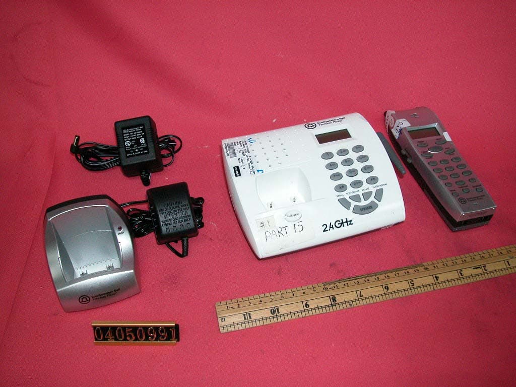
LBBGH3128AT
Jul 25, 20042.4GHz 40 Channel Cordless Phone w/ CID
Equipment Class
DXT - Part 15 Low Power Transceiver, Rx Verified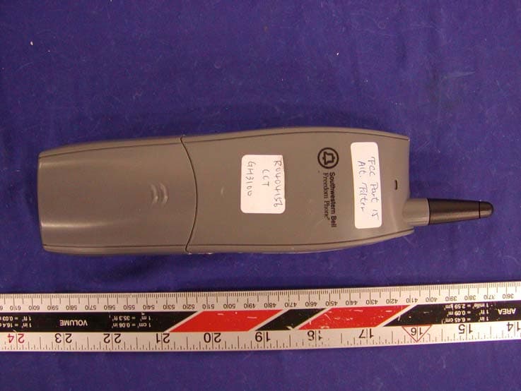
LBBGH3100H
May 06, 2004Cordless Phone
Equipment Class
DXX - Part 15 Low Power Communication Device Transmitter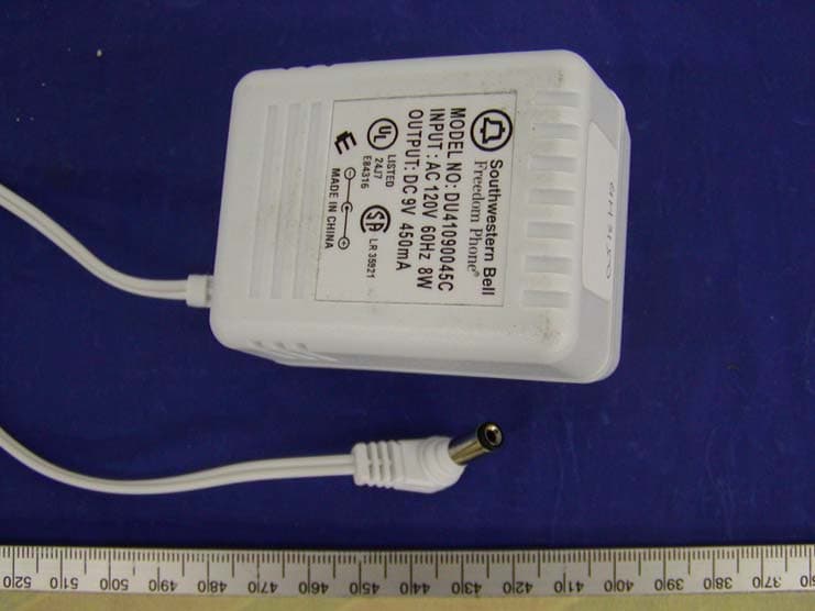
LBBGH3100
May 06, 2004Cordless Phone
Equipment Class
DXX - Part 15 Low Power Communication Device Transmitter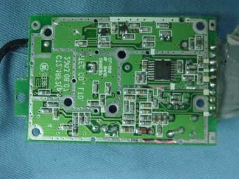
LBBGH3062
Apr 25, 20042.4 GHz Cordless Phone with Radio
Equipment Class
DXX - Part 15 Low Power Communication Device Transmitter
LBBGH4100
Apr 05, 20042.4GHz FHSS Cordless Phone w/ CID
Equipment Class
DSS - Part 15 Spread Spectrum Transmitter