LD7IGEN13.56 RFID Module
Xerox Corporation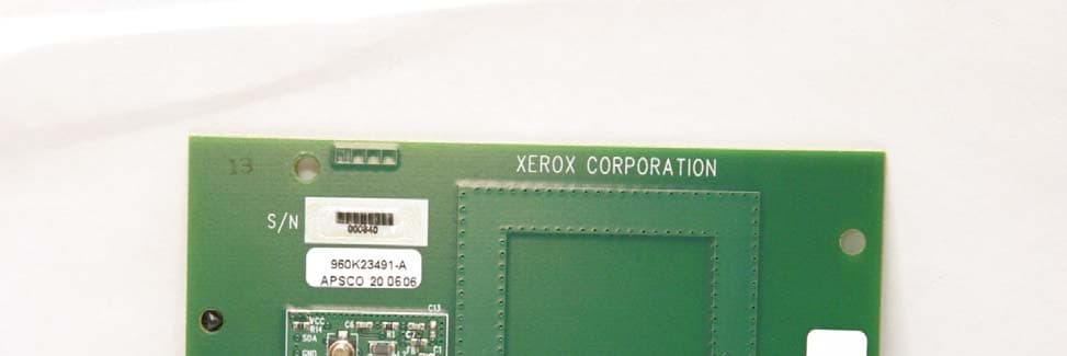
Click to zoom
Application Details
- Equipment Class
- DXX - Part 15 Low Power Communication Device Transmitter
- Date of Grant
- Dec 20, 2007
- Application Purpose
- Original Equipment
- Date of Application
- Dec 20, 2007
- Equipment Note
- 13.56 RFID Module
- Frequency Range
- 13.56000000 - 13.56000000
- Company
- Xerox Corporation
- Country
- United States
Documents & Files
Document Text
Text extracted from the exhibit documents filed with the FCC. Open a document above to read the original.
Users Manual
1 User Manual – IGEN Coupler Board 1.0 System Components There are two components, not including the driving host computer and the power supply, of the Radio Frequency CRUM Sub-System; the IGEN Coupler board (PWBA) and the RF memory tag (TAG). The PWBA is controlled by a host computer which sends commands and data to the PWBA. The PWBA then converts the commands into radio frequency actions which allow communication to the TAG. 1.1 IGEN Coupler Board The photo below shows the PWBA. The two connectors on the left side of the board are used for power input, addressing and communication. 2 1.2 RF Memory Tag (TAG) The TAG is a memory device which is mounted on a flexable substrate. The memory device is surrounded by a copper antenna also on the substrate. Through this antenna, power for the memory device and it’s associated controlling hardware is obtained from the RF signal generated by the PWBA. 2.0 Applying power to the PWBA (refer to the schematic for this discussion). Power is applied to the PWBA through the 6 pin connector (5volts DC) or the 10 pin connector (7.5 volts DC). The 6 pin connector receives 5 volts on pin 1 (5volts) and pin 3 (ground). The 10 pin connector receives 7.5 volts on pins 9, 10 (7.5 volts) and pin 8 (ground). Note that the board cannot operate from both supply voltages at one time. 3.0 Board Addressing Up to 8 PWBA’s can be communicated to by the host computer by using the three address lines (ADD_E0, ADD_E1 and ADD_E2). These address lines are tied into the 6 pin and the 10 pin interface connectors. If the addressing lines are left open, address 0 will be selected. External address jumpers select the remaining addresses in a binary fashion (refer to the schematic for details). 4.0 Sample Communication Protocol, IGEN Coupler Board to RF Memory Tag (Note: The details of the communication protocol are beyond the scope of this document. This is just a high level overview). The host processor board switches power on to the PWBA’s. A 100 milli-second stabilization time is waited. The RF field ON command is sent from the host processor to the PWBA to be communicated to. 3 The “find memory tag” command is sent from the host processor to the PWBA. The addressed PWBA generates an RF signal to find a TAG which could be in it’s field. After a TAG is found, a “select memory tag” command is sent from the host processor to the PWBA. Note that the PWBA converts the command into an RF signal for the TAG. Using a custom protocol, the host processor, the PWBA and the TAG transfer data blocks as required. The RF field OFF command is sent from the host processor to the PWBA. The host processor board removes power from the PWBA’s to end communication. 5.0 IGEN Coupler Board and RF Memory Tag Operation within a Xerox Printer The following illustrates one application for the IGEN Coupler board and RF Memory Tag as it would be used within a printing system. 5.1 RF Memory Tag Intallation on a Toner Bottle The photo below shows the RF memory tag mounted on a toner bottle. Note that unlike this photo, after the memory tag is mounted on the bottle cap, a protective label will be placed over the memory tag (not shown). Toner Bottle RF Memory Tag 4 5.2 RF Coupler Boards Mounted in a machine. The photo below shows 4 PWBA’s mounted in a machine. The memory tags associated with each PWBA are mounted on toner bottles behind the boards (cannot be seen in this photo). Toner Bottles behind these doors RF Coupler Board 5 5.3 Printer that houses the RF Coupler Boards and RF Memory Tags The RF Coupler Boards are located behind this door in the machine. 6 REGULATORY INFORMATION FCC PART 15 COMPLIANCE THIS DEVICE COMPLIES WITH PART 15 OF THE FCC RULES. OPERATION IS SUBJECT TO THE FOLLOWING TWO CONDITIONS: (1) THIS DEVICE MAY NOT CAUSE HARMFUL INTERFERENCE, AND (2) THIS DEVICE MUST ACCEPT ANY INTERFERENCE RECEIVED, INCLUDING INTERFERENCE THAT MAY CAUSE UNDESIRED OPERATION. MODIFICATIONS TO THE EQUIPMENT NOT EXPRESSLY APPROVED BY XEROX COULD VOID THE USER’S AUTHORITY TO OPERATE THE EQUIPMENT. ANY HOST DEVICE THAT CONTAINS THIS MODULE IS REQUIRED TO CLEARLY STATE THE FOLLOWING ON THE OUTSIDE OF THE HOST DEVICE: “CONTAINS FCC ID: LD7IGEN”. Marty Oksenhorn XEROX CORPORATION 12/10/07
Cover Letter(s)
December 4, 2007 To: SIEMIC, INC. 2206 Ringwood Avenue, San Jose, CA 95131 USA Dear Sir/Madam, Re: Project and Product Certification Representative Authorization Letter We, Xerox Corporation, hereby authorize SIEMIC, INC. to act as a Certification Body for certifying for the following project(s): (13.56 RFID Module, Model IGEN) We affirm that between SIEMIC and Xerox Corporation, any difference in understanding, including test plan, measurement methods, applicable standards and relevant procedures and processes have been resolved prior to commencement of testing activities. Sincerely, Gary Myers, Xerox EMC Manager Xerox Corporation 800 Phillips Rd, Building 205-99P Webster, NY 14580
Cover Letter(s)
Siemic Inc 2206 Ringwood Avenue San Jose, CA 95131 Date: December 4, 2007 RE: FCC ID: LD7IGEN Dear Reviewer: The following items are intended to show compliance with the requirements for a Part 15 modular transmitter approval for the 13.56 MHz transmitter under consideration in this filing. 1. The modular transmitter will be shielded inside the host units. Since this unit will be installed in Xerox printers control of this shielding will be maintained by the grant holder. 2. The modular transmitter only has data inputs inductively coupled via the toner cartridge tag assembly. This will ensure that no conditions of excessive data rates or over-modulation can occur. 3. The modular transmitter receives its DC power from a regulated supply from within the host and has an on board regulator as well. 4. The transmitter has an integral antenna. 5. The transmitter was tested in a stand-alone configuration. 6. The transmitter is labeled with its own FCC ID. The users manual contains instructions for host unit exterior labeling to use: “Contains FCC ID:” 7. The transmitter complies with all operating requirements applicable to the transmitter. 8. The transmitter complies with applicable RF exposure requirements. If there are additional questions please contact me. Sincerely Gary E. Myers Xerox EMC manager
Cover Letter(s)
2206 Ringwood Avenue San Jose, CA 95131 Tel: 408-526-1188 Fax: 408-526-1088 Email: [email protected] Correspondence Summary Q & A December 21, 2007 SUBJECT: XEROX CORPORATION - FCC ID: LD7IGEN Question about additional justification needed for Modular approval - RF shield requirement of item 1 of DA001407. Answer: The module complies with the radiated emissions requirements for the applicable rule parts in its current state. Additional shielding to satisfy these requirements is not necessary. Furthermore, this particular module has a specific installation configuration. The module will be attached to the metal L-bracket as shown in the operational description. The purpose of the module will be to exchange information with the toner bottle inside a copier or printer. As a result the side of the module not facing the Lbracket will be facing the toner cartridge. The typical implementation of this module will be such that there no cables directly over or under the module that may be coupled to. Please reference the user manual to see the typical installation of the module. Additionally, the relatively low power intentionally radiated by the equipment should also help to reduce the probability of unintended coupling within host devices. SIEMIC, INC. 2206 Ringwood Ave., San Jose, CA 95131 408-526-1188 Ext 207 [email protected]
Cover Letter(s)
IGEN Coupler Board Antenna Information The RF antenna is etched in copper on layer two of the circuit board. The antenna is a dual loop copper trace surrounded by a copper shield. Layer one (top layer), layer three and layer four (bottom layer) of the circuit board contain antenna shields etched in copper. Dual Loop Copper Antenna – Layer two RF input to the antenna loop Antenna Shield Antenna Shield – Layer 1 and Layer 4 Antenna Shield – Layer 3 Marty Oksenhorn XEROX CORPORATION 12/5/07
Cover Letter(s)
December 6, 2007 To: Federal Communications Commission Authorization and Evaluation Division Confidentiality Request regarding application for certification of FCC ID:LD7IGEN We hereby request confidential treatment of information accompanying this application as outlined below: - Schematics - Block Diagram - Operational Description - Technical Specification The above materials contain trade secrets and proprietary information not customarily released to the public. The public disclosure of these materials may be harmful to the applicant and provide unjustified benefits to its competitors. The applicant understands that pursuant to Section 0.457 and 0.459 of the Rules, disclosure of this application and all accompanying documentation will not be made before the date of the Grant for this application. Sincerely, Gary Myers, Xerox EMC Manager Xerox Corporation 800 Phillips Rd, Building 205-99P Webster, NY 14580
ID Label/Location Info
IGEN Coupler Board FCC / IC Label Location and Artwork 1.0 FCC/IC Label Artwork and Location Drawing 1.1 The photo below contains the FCC/IC label location on the board. 1.2 The label is to be a Weber L62403 label with the following text: FCC ID: LD7IGEN IC: 482B-IGEN 2.0 FCC/IC Label Artwork Sample Marty Oksenhorn XEROX CORPORATION 12/5/07 Label Location on the IGEN Coupler Board FCC ID: LD7IGEN IC: 482B-IGEN
ID Label/Location Info
IGEN Coupler Board FCC / IC Label Location and Artwork 1.0 FCC/IC Label Artwork and Location Drawing 1.1 The photo below contains the FCC/IC label location on the board. 1.2 The label is to be a Weber L62403 label with the following text: FCC ID: LD7IGEN IC: 482B-IGEN 2.0 FCC/IC Label Artwork Sample Marty Oksenhorn XEROX CORPORATION 12/5/07 Label Location on the IGEN Coupler Board FCC ID: LD7IGEN IC: 482B-IGEN
Test Report
XEROX Test Plan / Report EMC Group Compliance Log Number: EMC07025 Page 1 of 29 Form 2 EMC Test Group FCC Part 15, Subpart C and Industry Canada RSS-210 Compliance Report for Xerox Corporation Short Range Radio Frequency Identification (RFID) Device Model: IGEN Judgement: The Equipment Under Test (EUT) met the requirements specified in FCC Part 15, Subpart C, Sections 15.207, 15.209 and 15.225, and Industry Canada RSS-GEN, Sections 6 and 7.2.2. Accreditation Certificate Number: 1248-01 Electrical (EMC) Testing This laboratory is accredited by the American Association for Laboratory Accreditation (A2LA) and the results shown in this test report have been determined in accordance with the laboratory’s terms of accreditation unless stated otherwise in the report. The client is hereby notified that products, materials or other items in this report are in no way approved or endorsed by A2LA unless A2LA explicitly permits such endorsement or approval. XEROX Test Plan / Report EMC Group Compliance Log Number: EMC07025 Page 2 of 29 Form 2 XEROX Test Plan / Report For EUT NAME TEST PLAN NUMBER DATE IGEN EMC2007025 November 28, 2007 Abstract: This report documents the testing completed on an RFID Model IGEN as supplied by the client. The EUT was found to conform with the Federal Communications Commission, and Industry Canada regulatory limits for an intentional radiator and low power licence-exempt radiocommunication device, respectively. FCC is an acronym for “Federal Communications Commission. The FCC acronym is used throughout the document in lieu of the CFR 47 Part 15 Subpart C terminology. The IC acronym is used throughout the document in lieu of the Industry Canada RSS-GEN and RSS-210 terminology. Summary of Results Test Result Modifications required to pass Conducted Emissions Pass AC Line filter Radiated Emissions Pass None NAME TITLE SIGNATURE DATE Prepared By David Spencer EMC Engineer David Spencer 11/29/07 Approved By Gary E. Myers EMC Group Manager 11/29/07 XEROX Test Plan / Report EMC Group Compliance Log Number: EMC07025 Page 3 of 29 Form 2 Table Of Contents TEST PLAN SECTIONS 1-8___________________________________________________________ 5 1 CLIENT INFORMATION__________________________________________________________ 5 2 EMC TEST LABORATORY________________________________________________________ 5 3 EQUIPMENT UNDER TEST_______________________________________________________ 5 3.1 Identification of EUT______________________________________________________________ 5 3.2 Identification of Tested Optional Devices / Accessories___________________________________ 5 3.3 Physical Information______________________________________________________________ 5 3.4 Interface Ports___________________________________________________________________ 5 3.5 Description of the EUT____________________________________________________________ 5 3.6 Potential Emission Sources_________________________________________________________ 5 3.7 New Parts or Modifications Incorporated in the EUT____________________________________ 5 3.8 Support Equipment_______________________________________________________________ 5 4 TEST SPECIFICATIONS & PROCEDURES_______________________________________ 5 4.1 General_________________________________________________________________________ 5 4.2 Methods and Procedures___________________________________________________________ 5 4.3 Test Equipment__________________________________________________________________ 5 4.4 Test Facility_____________________________________________________________________ 5 4.5 Test Methodology_________________________________________________________________ 5 4.5.1 Conducted Emissions______________________________________________________________ 5 4.5.2 Radiated Emissions_______________________________________________________________ 5 5 CONFIGURATION & OPERATION OF EUT DURING TEST_______________________ 5 5.1 Configuration____________________________________________________________________ 5 5.2 Operating Environment____________________________________________________________ 5 5.3 Special Operating Requirements_____________________________________________________ 5 5.4 Operating Modes_________________________________________________________________ 5 5.5 Monitoring of the EUT____________________________________________________________ 5 6 DETAILED TEST PLAN___________________________________________________________ 5 6.1 Test Plan________________________________________________________________________ 5 6.1.1 Conducted Emissions______________________________________________________________ 5 6.1.2 Radiated Emissions_______________________________________________________________ 5 6.1.3 Frequency Stability_______________________________________________________________ 5 7 EMC MODIFICATION DETAILS__________________________________________________ 5 XEROX Test Plan / Report EMC Group Compliance Log Number: EMC07025 Page 4 of 29 Form 2 8 EMISSIONS COMPLIANCE CERTIFICATION____________________________________ 5 8.1 Judgment_______________________________________________________________________ 5 8.2 Filing__________________________________________________________________________ 5 8.3 Test Facility_____________________________________________________________________ 5 9 CONDUCTED EMISSIONS________________________________________________________ 5 9.1 Worse Case Run Mode_____________________________________________________________ 5 9.2 Measured Data___________________________________________________________________ 5 10 RADIATED EMISSIONS________________________________________________________ 5 10.1 Worse Case Run Mode_____________________________________________________________ 5 10.2 Measured Data___________________________________________________________________ 5 11 Frequency Stability_______________________________________________________________ 5 11.1 Run Mode_______________________________________________________________________ 5 11.2 Measured …
Text truncated - open the document above for the full version.
Contact Information
Applicant
Gary E Myers(Technical Specialist)
Test Firm
TUV Rheinland of North AmericaDavid Lanski
[email protected](585) 357-6044
Technical Specifications
| # | Rule Parts | Frequency Range | Power Output |
|---|---|---|---|
| 1 | 15C | 13.56 MHz - 13.56 MHz | - |
Other Applications from Xerox Corporation
LD7TLST
Nov 16, 2005RFID MODULE
Equipment Class
DXX - Part 15 Low Power Communication Device Transmitter
LD7JCMT
Nov 15, 2005RFID MODULE
Equipment Class
DXX - Part 15 Low Power Communication Device TransmitterLD7XNA-1
Oct 28, 1997JBP - Part 15 Class B Computing Device Peripheral
Equipment Class
JBP - Part 15 Class B Computing Device PeripheralLD7XTA-1
Jan 26, 1997JBP - Part 15 Class B Computing Device Peripheral
Equipment Class
JBP - Part 15 Class B Computing Device PeripheralLD7XCA-4
Jun 04, 1995Printer
Equipment Class
JBP - Part 15 Class B Computing Device Peripheral