LHJCNAD30To provide wireless connectivity within a vehicle
Continental Automotive Systems, Inc.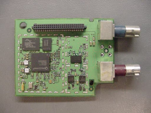
Click to zoom
Application Details
- Equipment Class
- PCB - PCS Licensed Transmitter
- Date of Grant
- Jan 27, 2010
- Application Purpose
- Original Equipment
- Date of Application
- Jan 27, 2010
- Equipment Note
- To provide wireless connectivity within a vehicle
- Frequency Range
- 1850.00000000 - 1910.00000000
- Country
- United States
Documents & Files
Document Text
Text extracted from the exhibit documents filed with the FCC. Open a document above to read the original.
Users Manual
User Manual for CNAD30 Doc No.: Rev: 0.1 Page 1 of 1 Operation Guide for CNAD3.0 CDMA Module 1. Product Overview CNAD3.0 is a CDMA module for use within automotive environment to provide wireless connectivity within a vehicle. The module will be integrated into a telematics device, which will be installed into a commercial vehicle during the car factory assembly process. The device has no user interface and will not be assessable without special tools. 2. Device Installation and User Manual The CNAD3.0 module is a proprietary product designed and manufactured by Temic Automotive North America, brand name Continental, for use by an automotive OEM. Because the CNAD3.0 is not intended for sale as a stand- alone device or offered for sale to general public, the user’s manual and sales brochure are not applicable to this product. 3. FCC Note This device complies with Part 22 and 24 of the FCC Rules. The FCC ID for this device is LHJCNAD30. Operation is subject to the following two conditions: 1. This device may not cause harmful interference. 2. This device must accept any interference received, including interference that may cause undesired operation. Changes or modifications to this system by other than an authorized service facility could void authorization to use this equipment. The device must be installed to provide a separation distance of at least 20cm from all persons and must not be co- located or operating in conjunction with any other antenna or transmitter.
External Photos
CNAD30 Continental Proprietary Confidential 1 Internal Photos for CNAD30 Fig. 1 Internal view: top side pcb with shields Fig. 2 Internal view: top side pcb without shields Fig. 3 Internal view: bottom side pcb with shields Fig. 4 Internal View: bottom side pcb without shields
ID Label/Location Info
FCC ID: LHJCNAD30IC: 2897E-CNAD30
ID Label/Location Info
FCC/IC Label Location
Internal Photos
CNAD30 Continental Proprietary Confidential 1 Internal Photos for CNAD30 Fig. 1 Internal view: top side pcb with shields Fig. 2 Internal view: top side pcb without shields Fig. 3 Internal view: bottom side pcb with shields Fig. 4 Internal View: bottom side pcb without shields
Operational Description
Operation Guide for CNAD3.0 Doc No.: Rev: 0.1 Page 1 of 5 Operation Guide for CNAD3.0 CDMA Device 1. Product Overview CNAD3.0 is a 1xRTT - capable device for use within automotive environment to provide wireless connectivity within a vehicle. The device will be installed behind the radio panel of a commercial vehicle during the car factory assembly process. The device has no user interface and will not be assessable without special tools. • Class II PCS band • Class III Cellular Band • 1x-RTT • SMS • On-board autonomous GPS • Fakra RF connector (violet) for GSM RF. • Fakra RF connector (blue) for GPS RF. • Automotive-grade system-level connector • Input Voltage 8-16 V 2. Device Installation and User Manual The CNAD3.0 device is a proprietary product designed and manufactured by Temic Automotive North America, brand name Continental, for use by an automotive OEM. Fig 1. Top view of CNAD3.0. Fig. 2 Bottom view of CNAD3.0 3. Special Testing Instructions Set-up requirements: [1] The interface board (NIB), its power cable, and 36 pin ribbon cable with 36 pin standoff. [2] 36 pin to 50 pin adapter circuit board. [3] 8V-16V Power supply capable of sourcing 1A. [4] A CDMA capable call box [Agilent 8960 is used in this example]. [5] A CNAD3.0 module Operation Guide for CNAD3.0 Doc No.: Rev: 0.1 Page 2 of 5 Figure 3. CNAD3.0 test set-up Power-up Instructions: [1] Program the power supply to 12V (acceptable range is 8V-16V) and set the current limit to 1.5A. IMPORTANT: Make certain the power supply output is off. [2] Connect the NIB to the power supply. [3] Connect the ribbon cable to the adapter board as shown in 4. Be certain that the ribbon cable is not backward. Fig. 4. Adaptor board and cable connection. [4] Connect the adapter board to the NAD as indicated in Figure 5. [5] Connect the serial communication cable to the NIB as shown in Figure 5. Operation Guide for CNAD3.0 Doc No.: Rev: 0.1 Page 3 of 5 Fig. 5. Properly assembled CNAD3.0 set-up [6] Launch Hyperterminal. Note: multiple applications trying to communicate on the same COM port will result in NO communication. [7] Turn on the power supply output. Current draw by the NIB should be around 95mA for NIBs with no LEDs, and 125mA for NIBS with LEDs. [8] Press the KBD_PWR switch down for about 1 second, then let go. The phone should power on. Current drawn from the power supply should jump by 20mA [9] Optionally connect USB as shown in Fig. 6 below, and launch QXDM or QPST for diagnostics. [10] Make sure the power is off before disconnecting the cables from the NIB. Making a Voice Call: [1] With the NAD connected as above, connect the RF cable to a call box. [2] Set the CDMA call parameter as indicated by the PRL. In this example, Band is US Cellular, Channel is 384, SID is 20, NID is 1. [3] For Auto-answer, Service Option 55 Loopback is used. For user answered calls, Service Option 3 Voice is used. [4] Wait for the NAD to register; this should be less than 30 seconds. [5] For mobile originated call, type ATD[number] e.g. ATD123 [6] For mobile terminated call, press the “originate call” soft-key. VOICE CALLS ONLY: The terminal will indicate the incoming call with “RING”. Type ATA to answer the call. Loopback calls will be auto-answered by the NAD. [7] To end the call, type ATH, or press the “end call” soft-key on the call box. Making a Packed Data Call: CNAD3.0 Serial Modem Driver Installation: [1] Save the Serial Modem driver file GEN7.2_modem.inf to local hard drive [2] Go to Start -> Settings -> Control Panel; [3] Double click on Phone and Modem Options; [4] Click on Modems and Add new modem; [5] Follow the windows system Add/Remove Hardware Wizard instructions and click on the Don’t detect my modem; I will select from a list option, then click on Next; [6] Click on Have Disk button, then click on Next; Operation Guide for CNAD3.0 Doc No.: Rev: 0.1 Page 4 of 5 [7] Click on Browse button to select the GEN7.2_modem.inf file just downloaded from local hard drive, then click on OK; [8] Choose Motorola CDMA 1X Modem from the Models list, then click on Next; [9] Specify the COM port needed to run the dial up connection, then click on Next; [10] Click on finish to complete the installation of Motorola serial modem driver. [11] Select Motorola CDMA 1X Modem, Click on the properties tab, and set the Maximum Port Speed to 115200 and ensure that the ‘Wait for Dialtone’ box is unchecked. Gen7.2_modem.inf CNAD6055 NAD Dial Up Networking Configuration: [1] Go to Start -> Settings -> Network and Dial Up connections -> Make New Connection; [2] Follow the windows system Network Connection Wizard instructions, Choose Dial up to private network option then click on Next; [3] Set the Phone number as #777 (please check using QPST service programming to insure #777 is configured as the Pkt Dial String in NAM), then click on Next; [4] Select the Connection Availability option to be For all users, then click on Next; [5] Name it as SO33 Dial Up Networking and click the option to create a shortcut on desktop, then click on Next; [6] The Connect SO33 Dial Up Networking window pops up and set both the user name and password to be same for testing with Racal or other settings specific to the network operator; [7] Click on the Properties button to change some configurations; [8] Under Security, check to enable Show terminal window under Interactive logon and scripting; [9] Under Networking, click on Settings button below PPP: Windows 95/98/NT 4/2000, Internet. Only select Enable software compression option. Click on OK; [10] Under general, click on Configure, and set the maximum speed to 115200bps. [11] Under general click on Configure, and make sure ‘Enable Hardware Flow Control’ is unchecked. [12] The Dial Up Networking configuration is complete. Powering off the NAD [1] Terminate the call if the NAD is connected. [2] Press KBD_PWR on the NIB for about 1 second. [3] Current drain should drop to 95mA [or 125mA for NIBs with LEDs] within 3 seconds indicating the NAD…
Text truncated - open the document above for the full version.
Test Report
This report is for the exclusive use of Intertek's Client and is provided pursuant to the agreement between Intertek and its Client. Intertek's responsibility and liability are limited to the terms and conditions of the agreement. Intertek assumes no liability to any party, other than to the Client in accordance with the agreement, for any loss, expense or damage occasioned by the use of this report. Only the Client is authorized to copy or distribute this report and then only in its entirety. Any use of the Intertek name or one of its marks for the sale or advertisement of the tested material, product or service must first be approved in writing by Intertek. The observations and test results in this report are relevant only to the sample tested. This report by itself does not imply that the material, product, or service is or has ever been under an Intertek certification program. TEST REPORT Report Number: 3190483LEX-001 Project Number: 3190483 Evaluation of the CNAD30 FCC ID: LHJCNAD30 Industry Canada ID: 2807E-CNAD30 FCC Part 22 Subpart H FCC Part 24 Subpart E FCC Part 15 Subpart B RSS-129 Issue 2 RSS-133 Issue 5 RSS-GEN Issue 2 For Continental Automotive Systems Test Performed by: Test Authorized by: Intertek 731 Enterprise Drive Lexington, KY 40510 Continental Automotive Systems 21440 West Lake Cook Road Deer Park, IL 60010 Prepared By:_______________________________Date:____12/6/2009________ Jason Centers, Senior Project Engineer Approved By:______________________________Date:____12/6/2009_________ Bryan Taylor, Team Leader – Engineering Intertek 731 Enterprise Drive, Lexington, KY 40510 Telephone: 859-226-1000 Fax: 859-226-1040 Web: www.etlsemko.com 731 Enterprise Drive, Lexington KY 40510 Evaluation For:Continental Automotive Systems FCC ID: LHJCNAD30 Model No: CNAD30 ICID:2807E-CNAD30 Report Number: 3190483LEX-001 Page 2 of 38 FCC Part 22H, 24E, and 15B Evaluation TABLE OF CONTENTS 1 JOB DESCRIPTION .......................................................................................................................... 4 1.1 COMPANY INFORMATION............................................................................................................ 4 1.2 TEST SAMPLE INFORMATION....................................................................................................... 4 1.3 SYSTEM SUPPORT EQUIPMENT.................................................................................................... 5 1.4 CABLES USED DURING TESTING................................................................................................. 5 1.5 SYSTEM BLOCK DIAGRAM(S) ...................................................................................................... 6 1.6 MODE(S) OF OPERATION / ENGINEERING JUDGMENTS................................................................ 6 2 EXECUTIVE SUMMARY................................................................................................................. 7 2.1 MODIFICATIONS REQUIRED FOR COMPLIANCE............................................................................ 7 3 TEST FACILITY................................................................................................................................ 8 3.1 TEST EQUIPMENT......................................................................................................................... 8 4 CONDUCTED RF POWER .............................................................................................................. 9 4.1 TEST PROCEDURE........................................................................................................................ 9 4.2 TEST RESULTS............................................................................................................................. 9 5 RADIATED RF POWER................................................................................................................. 10 5.1 TEST PROCEDURE...................................................................................................................... 10 5.2 TEST RESULTS........................................................................................................................... 10 6 MAXIMUM PERMISSIBLE EXPOSURE (MPE) CALCULATIONS ...................................... 11 6.1 CALCULATIONS.......................................................................................................................... 11 6.2 TEST RESULTS........................................................................................................................... 11 7 EMISSION LIMITATIONS, OCCUPIED BANDWIDTH .......................................................... 12 7.1 TEST PROCEDURE...................................................................................................................... 12 7.2 TEST RESULTS........................................................................................................................... 12 8 OUT OF BAND EMISSION AT ANTENNA TERMINALS........................................................ 14 8.1 TEST PROCEDURE...................................................................................................................... 14 8.2 TEST RESULTS........................................................................................................................... 15 9 RADIATED SPURIOUS EMISSIONS ........................................................................................... 33 9.1 TEST PROCEDURE...................................................................................................................... 33 9.2 TEST RESULTS........................................................................................................................... 33 10 RECEIVER SPURIOUS EMISSIONS ...................................................................................... 35 10.1 TEST LIMITS................................................................................…
Text truncated - open the document above for the full version.
Contact Information
Applicant
James Zhang
Technical Contact
Temic Automotive North America Inc.Irina Shmagin
[email protected]847-862-2420
21440 West Lake Cook Road · Deer Park, Illinois · United States
Non-Technical Contact
Temic Automotive North America Inc.James Zhang
[email protected]847-862-2235
Test Firm
Intertek Testing Services NAJames Sudduth
Technical Specifications
| # | Rule Parts | Frequency Range | Power Output | Emission | Tolerance |
|---|---|---|---|---|---|
| 2 | 24E | 1.85 GHz - 1.91 GHz | 320.00 mW | 1M25F9W | 22 Hz |
Other Applications from Continental Automotive Systems, Inc.
LHJ-FE5RW0020
May 15, 2026FE5RW0020
Equipment Class
PCB - PCS Licensed Transmitter
LHJ-HM28NA001
May 04, 2023HM28NA-001
Equipment Class
CXX - Communications Rcvr for use w/ licensed Tx and CBs
LHJ-FE3RW0051
Jan 07, 2023FE3RW0051
Equipment Class
CXX - Communications Rcvr for use w/ licensed Tx and CBs
LHJ-BL28NARD2
Dec 14, 2022BL28NA-RD2
Equipment Class
PCB - PCS Licensed Transmitter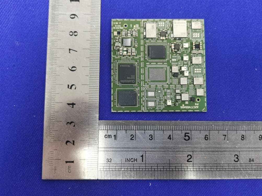
LHJ-FE5NA0010
Nov 09, 2022FE5NA0010,FE5NA0011
Equipment Class
JBP - Part 15 Class B Computing Device Peripheral