LYIAT7200200W UHF ATSC Transmitter - Advanced TV
Hitachi Kokusai Electric America LTD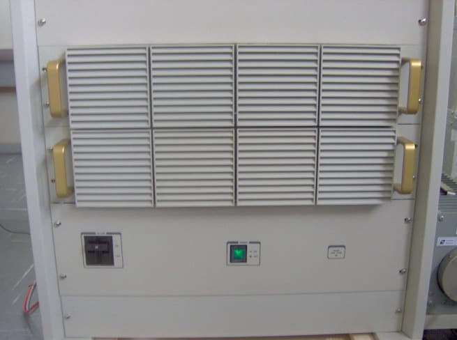
Click to zoom
Application Details
- Equipment Class
- TBC - Licensed Broadcast Station Transmitter
- Date of Grant
- Dec 12, 2006
- Application Purpose
- Original Equipment
- Date of Application
- Dec 12, 2006
- Equipment Note
- 200W UHF ATSC Transmitter - Advanced TV
- Frequency Range
- 614.00000000 - 806.00000000
- Country
- United States
Documents & Files
Document Text
Text extracted from the exhibit documents filed with the FCC. Open a document above to read the original.
Users Manual
AT7400Owner Manual Rev. 2.0– October 2006-10 -231/1 1 ADVANCED TV LINE Model AT7200 200W ATSC UHF Transmitter OWNERS MANUAL Linear Industries Incorporation www.linear-tv.com Made in USA AT7400Owner Manual Rev. 2.0– October 2006-10 -231/1 1 AT7200 200W ATSC DTV TRANSMITTER ADVANCED TV LINE Owner Manual Table of Contents Section 1:Technical Specifications Typical Final Test Report Section 2:Master Control Unit Section 3:Exciter Drawer Section 4:Intermediate Directional Coupler Section 5:220W UHF Power Amplifier Section 6:Output Directional Coupler, and Filtering Section 7:Energy Distribution and Control Annex A:Schematics Diagrams AT7400Owner Manual Rev. 2.0– October 2006-10 -231/3 User Notices and WARNINGS USER NOTICES IT IS VERY IMPORTANT TO READ THE FOLLOWING MANUAL SECTIONS PRIOR TO OPERATION OF THIS TRANSMITTER! Notice 1 The transmitter main operating voltage setting is marked on the rear of the AT7250 chassis. Notice 2 The transmitter operating frequency is set from the factory. Notice 3 For adjusting the RF output power setting aqualified technician should always employ the use of an RF Wattmeter and a calibrated dummy load. Notice 4 Should accident or injury occur to the personnel engaged in the installation, operation, or service of the equipment should seek proper medical attention. It is advisable that such personnel have familiarity with first-aid practices. Notice 5 To call our technical support center or for other customer service issues at Linear Inc, refer to the following number: 630 346 6698. Notice 6 If you experience some specific difficulty and the technical information available in this manual is not enough to help you, do not hesitate to call LINEAR technical support center. Notice 7 The technical information presented on this manual is sole intellectual propriety of LINEAR INDUSTRIES Inc. Reproduction of this document in full or partial is prohibiting with out written authorization. This document is legally protected by the copy rights laws. AT7400Owner Manual Rev. 2.0– October 2006-10 -232/3 WARNING! THE VOLTAGES AND CURRENTS IN THIS EQUIPMENT ARE DANGEROUS.PERSONEL MUST, AT ALL TIMES, OBSERVE SAFETY WARNINGS, INSTRUCTIONS, AND ANY REGULATIONS. THIS OWNER’S MANUAL IS INTENDED AS A GENERAL GUIDE FOR TRAINED AND QUALIFIED PERSONNEL WHO ARE AWARE OF THE DANGERS THAT ARE INHERENT IN THE HANDLINGANDOPERATIONOFPOTENTIALLYHAZARDOUSELECTRICALAND ELECTRONIC CIRCUITS.IT IS NOT THE INTENT OF THIS MANUAL TO PROVIDE A COMPLETE SET OF SAFETY INSTRUCTIONS OR PRECAUTIONS THAT SHOULD ALREADY BE UNDERSTOOD BY TRAINED OR EXPERIENCED PERSONNEL IN USING THIS OR OTHER TYPES OF ELECTRONIC EQUIPMENT. THE INSTALLATION, OPERATION, AND MAINTENANCE OF THIS EQUIPMENT INVOLVE RISKS TO PERSONNEL AND ALSO TO THE EQUIPMENT. LINEAR, INC. SHALL NOT BE RESPONSIBLE FOR INJURY OR DAMAGE THAT IS THE RESULT OF IMPROPER PROCEDURESOR USE BY PERSONS IMPROPERLY TRAINED OR LACKING THE KNOWLEDGE TO PERFORM ASSOCIATED TASKS. ALL LOCAL CODES FOR BUILDING, SAFETY, FIRE, OR RELATED STANDARDS MUST BE OBSERVED. CONSULT LOCAL AUTHORITIES FOR THE STANDARDS FOR THE AREA OR REGION WHERE THE EQUIPMENT WILL BE INSTALLED AND PUT IN USE. WARNING! AT ALL TIMES DISCONECT AC/MAINS POWER BEFORE OPENING COVERS, DOORS, ENCLOSURES, PANELS, OR PROTECTIVE SHIELDS THAT EXPOSE LIVE CIRCUITS. NEVER PERFORM MAINTENANCE, MAKE ADJUSTMENTS, OR SERVICE THE EQUIPMENT WHEN ALONE OR FATIGUED. WARNING! IF ELECTROLYTIC OR OIL FILLED CAPACITORS ARE UTILIZED IN THE EQUIPMENT AND THE COMPONENT APPEARS LEAKY, OR IS BULGING, OR IF THE CASE OR COVERING OF THE COMPONENT APPEARS DAMAGED OR DISTRESSED ALLOW SUFFICIENT TIMEFOR THE UNIT TO COOL OR FULLY DISCHARGE BEFORE SERVICING. SERVICING HOT OR LEAKY CAPACITORS CAN CAUSE A RUPTURE OF THE CASE AND POSSIBLE INJURY. AT7400Owner Manual Rev. 2.0– October 2006-10 -233/3 Returns and Exchanges Equipment (Damaged or undamaged) should not be returned unless written approval and a Merchandise Return Authorization (MRA Number) is received from your Linear Sales representative orLinearCustomer Service.Special shipping instruction will be provided which will assure proper handling. The circumstances and reasons for the returnmust be included in the request for return. Equipment that is special or “custom” ordered may be not returnable. In situations where return or exchange is at the request of the customer a restocking fee may be charged. All returns must be sent freight prepaid and properly insured by customer. When communicating withLinearplease refer to your Order or Invoice Number. Unpacking Use care when unpacking the equipment. First perform a visual inspection of the item(s) to determine if any damage occurredduring shipment. Be sure to retain all the shipping materials (crates and boxes or cartons) until such time that it has been determined that the received equipment arrived undamaged. Find all PACKING LISTS and keep them to assist in locating and identifying any components or assemblies that may have been removed for shipping and might need to be reinstalled in the equipment. Make sure that all shipping straps, supports and packing materials are completely removed from the equipment prior to initialization and use. AT7400Owner Manual Rev. 2.0– October 2006-10 -23Section 1- 1/7 1 Section 1– AT7200 Technical Specifications 1.Introduction The AT7200 is a 200W UHF ATSC/8VSB transmitter assembled and tested in United States by LINEAR INDUSTRIES INC. (www.linear-tv.com). Fig1.1: AT7200 Front View, cabinet wheels are optional. AT7400Owner Manual Rev. 2.0– October 2006-10 -23Section 1- 2/7 2 2.AT7200 RF line Up: 3.AT7200 Cabinet Air Flux: 0.25m 3 /sec.- 21ft 3 /sec. Fig. 1.4: Air flux path at AT4700 cabinet, (lateral view). Darker area denotes the internal heat source, or the RFdrawers, (1) Exciter and (2) PA’s. Cold Air Inlet Air Outlet AT7400Owner Manual Rev. 2.0– October 2006-10 -23Section 1- 3/7 3 4.AT7200– 200W UHF ATSC/8VSB Transmitter- Technical Specifications Electrical Main220/240 VAC, bi phase, 50-60 Hz…
Text truncated - open the document above for the full version.
Users Manual
AT7400Owner Manual Rev. 2.0– October 2006-10 -23Section 3- 31 /39 A total of 8 main operational functions are performed by the circuitry assembled on the module 4456. Please refer to the module 4456 block diagram. 3.10.1.1Module 4456– CIM3347- Power Factor Corrector, PFC The PFC circuit is a power supply built according withthe “boost regulator in continuous mode (CCM)” topology. Under the CCM topology, is possible guarantee a power factor, cosφabove than 0.9. The PFC circuit is composed by a full diode bridge that performs a full-wave rectification on the AC signal, whichthan is routed to the boost inductor. The voltage is so boosted up to +385V. The power factor correction is obtained by the switching a MOSFET transistor, which controls the electrical current into the capacitors that are components of the output rectification filter. The switching operation is performed at the frequency of 100MHz. 3.10.1.1.1.CIM3427- PFC Control unit The PFC switching operation is controlled by a bit stream. This control’s bit stream is generated by an integrated circuit with 2 loops that are self-protected against short circuits. The function of this control is to keep stable the +385V voltage at the PFC’s output. 3.10.1.2CIM3447– Full Bridge- +32 VoltsFixed The full bridge circuitry is also located at the PCB CIM 3447 as part of the module 4456. This circuit is designed to step down the +385V to +32V keeping the same power rate, meaning it enable the voltage to delivery more electrical current. The full bridge topology is favorable to high power management operations. The circuit has 4 transistors technology IGBT, (Insulated Bipolar Gate Transistor). Via a step down high current transformer, the high voltage, 100 kHz, pulses are reduced down to +32V, in sequence than rectified and filtered, becoming the +32 FIXED voltage. 3.10.1.3+15VoltsDirect The +15VDirect is a linear power supply circuit located at the PCB CIM 3447. A power transformer is directly connected to the 208 VAC mains. From this power supply is extracted: (A) +15VDc voltage that feeds the SCU (CIM 3297) exclusively, (B) +18VDc routed tothe control of the PFC circuit, located at CIM 3447 (C) +15VDc routed to the full bridge control, located also at the CIM 3447. 3.10.1.4FullBridgeControl andOutputVoltageReading The PCB CIM 3429, functionally associated to the CIM 3447, is in charge to generate the pulses that will control the full bridge circuitry. On this PCB is located the trim pot TPO-1 that adjust the +32V. On this PCB is also located the trim pot TPO-2 that adjust the over current protection. A third function is the voltage sensor reading circuit, which can be adjusted by the trim pot TPO-3. The output of this sensor is routed to the SCU, PCB CIM 3297. AT7400Owner Manual Rev. 2.0– October 2006-10 -23Section 3- 32 /39 3.10.1.5Shut Down When an abnormal failure situation occurs inside the exciter drawer, the SCU generate a SHUT DOWN command that is a +5Vdirect connected to the pin # 1 at the connector CON-5 located at the PCB CIM 3429. Since this voltage is present, the switching pulses will be inhibit and as consequence, all the DC output available at the sub- module 4456 will be disabled and be no longer available, exception for the +15Vdc DIRECT, that feeds the SCU. IMPORTANT: On maintenance situation the module 4456 the automatic operation, AUT, can be turned on a manual MAN, operation by changing the position of the jump CON-3. The SHUT DOWN commandas a protection it is always set as 0V at the PCB CIM 3297. 3.10.1.6Re-powering theTransmitter ON Considering the UHF exciter drawer the +32V ON/OFF associated to the sub-module 4456 is used exclusively to feed the 75W RF pallet amplifiers, sub-module 4451. From the +32V FIXED output, derives the +32V ON/OFF which is controlled by the SCU via the re-power up command. During normal conditions the re-power up command send a +5V voltage to the pin #2 at the connector CON-5 located at the PCB CIM 3429, part of thesub-module 4456. At the presence of this command, one transistor will be saturated and as consequence, the +32V ON/OFF out put will be enabled. The re-power up +5V command will always be present as an output from the PCB CIM 3297. 3.10.1.7Buck Converters There are 3 buck converters located at the sub-module 4456. The +32V FIXED feeds these 3 circuits simultaneously, responsible for the following DC voltages: +2.5V @ 5A– PCB CIM 3460. +5V @ 5A– PCB CIM 3459. +15V @ 2A and-15V @ 200mA– CIM 3461 AT7400Owner Manual Rev. 2.0– October 2006-10 -23Section 3- 33 /39 3.10.1.8Module 4456– Technical Specifications 3.11.PCB CIM3297– Subordinate Control Unit (SCU) on Module 4456 The module 4456 is equipped with its own control unit. This control unit is assembled as the same of the master control unit MCU, both CIM3297, however the software that runs each one are not the same. The SCU is on constant two ways communication with the MCU. Fig.3.14: SCU assembled at the exciter drawer GV4456– module 4456 AT7400Owner Manual Rev. 2.0– October 2006-10 -23Section 3- 34 /39 ( V L ) + 3 2 V O U T P U T V O L T A G E R E A D I N G → P I N 4 – C O N - 5 – C I M 3 4 2 9 – M O D . 4 4 5 6 – P O W E R S U P P L Y ( W H ) G N D → C O N - 1 6 – C I M 3 4 4 7 – M O D . 4 4 5 6 – P O W E R S U P P L Y ( V L ) S E R I A L D A T A O U T → P I N 6 – C O N 1 – C I M 3 4 5 6 – M O D . 4 4 6 6 – D D S ( Y L ) E X C I T E R T E M P E R A T U R E A L A R M → P I N 6 – C O N - 1 – C I M 3 4 4 6 – M O D . 4 4 5 3 – 3 0 W U H F E X C I T E R ( B R ) V C O 1 C O N T R O L → P I N 1 – C O N - 2 – C I M 3 4 4 3 – M O D . 4 4 5 3 – U H F U P C O N V E R T E R ( G R ) I O U P D A T E C L O C K → P I N 3 – C O N - 1 – C I M 3 4 5 6 – M O D . 4 4 6 6 – D D S ( R D ) D I V 5 → P I N 3 – C O N - 1 – C I M 3 4 4 3 – M O D . 4 4 5 3 – U H F U P C O N V E R T E R ( V L ) D I V 4 → P I N 4 – C O N - 1 – C I M 3 4 4 3 – M O D . 4 4 5 3 – U H F U P C O N V E R T E R ( B K ) D I V 3 → P I N 5 – C O N - 1 – C I M 3 4 4 3 – M O D . 4 4 5 …
Text truncated - open the document above for the full version.
Users Manual
AT7400Owner Manual Rev. 2.0– October 2006-10 -23Section 5-14 /17 7.2.Board CIM3452Schematic Diagram: SEE ANNEX A 8.GAV4445- Module 4275– Power Supply 8.1.Module 4275– General Functional Description Module 4275 is a switching high power DC supply, type full-bridge powered by 208 Vac, showing overall efficiency above 80%. As part of the power supplydesign, there is a power factor corrector, PFC, circuit. Besides correct the power factor to close to 1, this circuit also contributes to reduce the harmonic content returning from the unit into the AC mains. The sub-module 4275 deliveries two +32V voltage outputs, VA and VB. These two voltages feeds the 75W UHF amplifiers, sub-module 4451. This sub-module also delivery the +15V for the control unit SCU, CIM 3452, located on the power drawer. The module 4275 is composed by the following PCB’s: Fi g.5.9: CIM3429– Full Bridge Control PCB. AT7400Owner Manual Rev. 2.0– October 2006-10 -23Section 5-15 /17 8.2.GAV4445– Module 4275– Block Diagram R E T I F I E R S + 3 8 5 V I N D U C T O R S W IT C H I N G T R A N S I S T O R S R E T I F I E R F I L T E R S 1 8 0 t o 2 6 0 V A C G R O U N D P F C C O N T R O L C IM 3 4 2 7 + 1 8 V P O W E R F A C T O R C O R R E C T I O N ( P F C ) I G B T S W I T C H I N G T R A N S I S T O R S R E T I F I E R IN D U C T O R F U L L B R I D G E C O N T R O L C I M 3 4 2 9 F U L L B R I D G E + 1 5 V T R A N S F O R M E R F I L T E R + 3 2 V + 3 2 V R E S T A R T E D P U L S E T R A N S F O R M E R G R O U N D R E T I F IE R S T R A N S F O R M E R + 1 5 V R E G U L A T O R + 1 8 V R E G U L A T O R + 1 5 V O U T P U T + 1 8 V T O P F C C O N T R O L + 1 5 V T O F U L L B R I D G E C O N T R O L S U P P L I E S T O P F C C O N T R O L A N D F U L L B R I D G E C O N T R O L C I M 3 4 4 7 C I M 3 4 4 7 C I M 3 4 4 7 S H U T D O W N C O M M A N D E R R E C O N E C T I O N C O M M A N D E R F R O M S C U C I M 3 2 9 7 S W IT C H T R A N S IS T O R + 2 . 5 V + 2 . 5 V B U C K C O N V E R T E R C I M 3 4 6 0 + 5 V + 5 V B U C K C O N V E R T E R C I M 3 4 5 9 - 1 5 V + 1 5 V / - 1 5 V B U C K C O N V E R T E R C I M 3 4 6 1 + 1 5 V R E T I F I E R S + 3 8 5 V I N D U C T O R S W IT C H I N G T R A N S I S T O R S R E T I F I E R F I L T E R S 1 8 0 t o 2 6 0 V A C G R O U N D P F C C O N T R O L C IM 3 4 2 7 + 1 8 V P O W E R F A C T O R C O R R E C T I O N ( P F C ) I G B T S W I T C H I N G T R A N S I S T O R S R E T I F I E R IN D U C T O R F U L L B R I D G E C O N T R O L C I M 3 4 2 9 F U L L B R I D G E + 1 5 V T R A N S F O R M E R F I L T E R + 3 2 V + 3 2 V R E S T A R T E D P U L S E T R A N S F O R M E R G R O U N D G R O U N D R E T I F IE R S T R A N S F O R M E R + 1 5 V R E G U L A T O R + 1 8 V R E G U L A T O R + 1 5 V O U T P U T + 1 8 V T O P F C C O N T R O L + 1 5 V T O F U L L B R I D G E C O N T R O L S U P P L I E S T O P F C C O N T R O L A N D F U L L B R I D G E C O N T R O L C I M 3 4 4 7 C I M 3 4 4 7 C I M 3 4 4 7 S H U T D O W N C O M M A N D E R R E C O N E C T I O N C O M M A N D E R F R O M S C U C I M 3 2 9 7 S W IT C H T R A N S IS T O R + 2 . 5 V + 2 . 5 V B U C K C O N V E R T E R C I M 3 4 6 0 + 5 V + 5 V B U C K C O N V E R T E R C I M 3 4 5 9 - 1 5 V + 1 5 V / - 1 5 V B U C K C O N V E R T E R C I M 3 4 6 1 + 1 5 V AT7400Owner Manual Rev. 2.0– October 2006-10 -23Section 5-16 /17 8.3.CIM3238– Power Phase Control Unit– PFC The PFC circuit is located at PCB CIM 3238, at sub-module 4275.The PFC circuit is a power supply built according with the “boost regulator in continuous mode (CCM)” topology. Under the CCM topology, is possible guarantee a power factor, cosφabove than 0.9. The PFC circuit is composed by a full diode bridge that performs a full-wave rectification on the AC signal, which than is routed to the boost inductor. The voltage is so boosted up to +385V. The power factor correction is obtained by the switching a MOSFET transistor, which controls the electrical current into the capacitors that are components of the output rectification filter. The switching operation is performed at the frequency of 100MHz 8.3.8.CIM3427– PFC Control Unit The PCB CIM 3427 generates the control pulses for the PFC circuit.The PFC switching operation is controlled by a bit stream. This control’s bit stream is generated by an integrated circuit with 2 loops that are self-protected against short circuits. The function of this control is to keep stable the +385V voltage at the PFC’s output. 8.4.CIM3238– Full Bridge The full bridge circuitry is also located at the PCB CIM 3238 as part of the sub-module 4275. This circuit is designed to step down the +385V to +32V keeping the same power rate, meaning it enable the voltage to delivery more electrical current. The full bridge topology is favorable to high power management operations. The circuit has 4 transistors technology IGBT, (Insulated Bipolar Gate Transistor). Via a step down high current transformer, the high voltage, 100 kHz, pulses are reduced down to +32V, in sequence than rectified and filtered, becoming the two +32 FIXED voltages, (VA and VB). 8.5.CIM3238– Self-powered PowerSupply, and +15VDC Output The PCB CIM 3238 also delivery voltages for the PFC control circuits and full bridge. From this circuit is also generate the +15V to the SCU, PCB CIM 3452. The +15V Direct is a linear power supply circuit. A power transformer is directly connected to the 208 VAC mains. From this power supply is extracted (A) +15VDc voltage that feeds the SCU (CIM 3297) exclusively, (B) +18VDc feeds the control of the PFC circuit. The voltage +15VDc feed the full bridge control, and the SCU, PCB CIM 3452. 8.6.CIM3429– Full Bridge Control and Voltage Readings The module 4275 also holds the PCB CIM 3429. This circuit is in charge to generate the pulses that will control the full bridge circuitry. On this PCB is located the trim pot TPO-1 that adjust the +32V. On this PCB is also located the trim pot TPO-2 that adjust the over current protection. A third function is …
Text truncated - open the document above for the full version.
Users Manual
AT7400Owner Manual Rev. 2.0– October 2006-10 -23ANNEX ASection 7- 3/9 7.2.EnergyBi-PhaseDistribution andControl– Block Diagram T O P R A C K F A N L IN E A R E Q UI P A M E N T O S E L ET R Ô N I C O S LI N E A D I G IT A L T V [ S e tu p ] [ M e a s u re ] [ A la rm s ][ T e le s up ] M A I N C O N T R O L U N I T ( M C U ) M O D U L E 4 4 5 9 F A N F U S E S E N S O R ( F 1 ) P H A S E P R E S E N C E R S T M A I N T R I P H A S I C C O N T A C T O R R S T B A T T E R Y C H A R G E R D C / D C C O N V E R T E R 1 2 V / 7 A h B A T T E R Y M O D U L E 4 1 4 7 F A N F U S E S E N S O R F 1 + 1 5 V + 8 V 2 0 A B I I P O L A R M A I N B R A K E R I N T E R L O C K 1 2 0 V 1 2 0 V 1 2 0 V + 3 2 V 1 2 0 V 1 2 0 V S E C O N D A R Y B I P H A S I C C O N T A C T O R T I M E R 2 , 5 s D E L A Y 2 s S T A R T I N G S W I T C H 1 2 0 V 3x 18R / 50W P H A S E 1 P H A S E 2 P H A S E 3 N E U T R A L 1 2 0 V ( G Y ) 1 2 0 V ( R D ) G R O U N D P O W E R D R A W E R P O W E R S U P P L Y M O D U L E 4 2 7 5 +32V(VA) S E C O N D A R Y C O N T R O L U N I T C I M 3 4 5 2 2 0 8 V +8V +32V(VB) + 8 V 7 5 W U H F A T S C A M P L I F I E R 3 M O D U L E 4 4 5 1 + 3 2 V ( V A ) + 3 2 V ( V B ) 7 5 W U H F A T S C A M P L I F I E R 4 M O D U L E 4 4 5 1 + 3 2 V ( V A ) + 3 2 V ( V B ) 7 5 W U H F A T S C A M P L I F I E R 1 M O D U L E 4 4 5 1 + 3 2 V ( V A ) + 3 2 V ( V B ) 7 5 W U H F A T S C A M P L I F I E R 2 M O D U L E 4 4 5 1 + 3 2 V ( V A ) + 3 2 V ( V B ) G N D 3 0 0 W U H F A T S C P O W E R D R A W E R – P A 1 + 3 2 V E X C I T E R D R A W E R P O W E R S U P P L Y M O D U L E 4 4 5 6 3 0 W U H F A T S C E X C I T E R M O D U L E 4 4 5 5 3 0 W U H F A T S C E X C I T E R D R A W E R +15V + 1 5 V D I R S E C O N D A R Y C O N T R O L U N I T ( S C U ) C I M 3 2 9 7 U H F U P C O N V E R T E R M O D U L E 4 4 5 3 2 0 8 V + 3 2 V - 15V +12V +8V +5V +3,3V +1,2V +32V 8 V S B M O D U L A T O R M O D U L E 4 4 5 4 + 3 . 3 V + 1 . 2 V + 1 5 V + 5 V - 1 5 V D I R E C T D I G I T A L S Y N T H E S I Z E R ( D D S ) M O D U L E 4 4 6 6 + 1 5 V + 5 V + 5 V + 3 . 3 V + 1 5 V + 1 2 V - 1 5 V + 3 2 V + 5 V + 3 2 V + 1 2 V V O L T A G E R E G U L A T O R S M O D U L E 4 4 7 0 + 2 . 5 V + 1 . 2 V + 1 5 V + 5 V + 3 . 3 V + 1 2 V G N D 1 2 0 V 3x 18R / 50W 1 2 0 V 1 2 0 V 1 2 0 V T O P R A C K F A N L IN E A R E Q UI P A M E N T O S E L ET R Ô N I C O S LI N E A D I G IT A L T V [ S e tu p ] [ M e a s u re ] [ A la rm s ][ T e le s up ] L IN E A R E Q UI P A M E N T O S E L ET R Ô N I C O S LI N E A D I G IT A L T V [ S e tu p ] [ M e a s u re ] [ A la rm s ][ T e le s up ] [ S e tu p ] [ M e a s u re ] [ A la rm s ][ T e le s up ] M A I N C O N T R O L U N I T ( M C U ) M O D U L E 4 4 5 9 F A N F U S E S E N S O R ( F 1 ) P H A S E P R E S E N C E R S T M A I N T R I P H A S I C C O N T A C T O R R S T R S T M A I N T R I P H A S I C C O N T A C T O R R S T B A T T E R Y C H A R G E R D C / D C C O N V E R T E R 1 2 V / 7 A h B A T T E R Y 1 2 V / 7 A h B A T T E R Y M O D U L E 4 1 4 7 F A N F U S E S E N S O R F 1 + 1 5 V + 8 V 2 0 A B I I P O L A R M A I N B R A K E R I N T E R L O C K 1 2 0 V 1 2 0 V 1 2 0 V + 3 2 V 1 2 0 V 1 2 0 V S E C O N D A R Y B I P H A S I C C O N T A C T O R T I M E R 2 , 5 s D E L A Y 2 s D E L A Y 2 s S T A R T I N G S W I T C H 1 2 0 V 3x 18R / 50W3x 18R / 50W P H A S E 1 P H A S E 2 P H A S E 3 N E U T R A L 1 2 0 V ( G Y ) 1 2 0 V ( R D ) G R O U N D P O W E R D R A W E R P O W E R S U P P L Y M O D U L E 4 2 7 5 +32V(VA) S E C O N D A R Y C O N T R O L U N I T C I M 3 4 5 2 2 0 8 V +8V +32V(VB) + 8 V 7 5 W U H F A T S C A M P L I F I E R 3 M O D U L E 4 4 5 1 + 3 2 V ( V A ) + 3 2 V ( V B ) 7 5 W U H F A T S C A M P L I F I E R 3 M O D U L E 4 4 5 1 + 3 2 V ( V A ) + 3 2 V ( V B ) 7 5 W U H F A T S C A M P L I F I E R 4 M O D U L E 4 4 5 1 + 3 2 V ( V A ) + 3 2 V ( V B ) 7 5 W U H F A T S C A M P L I F I E R 4 M O D U L E 4 4 5 1 + 3 2 V ( V A ) + 3 2 V ( V B ) 7 5 W U H F A T S C A M P L I F I E R 1 M O D U L E 4 4 5 1 + 3 2 V ( V A ) + 3 2 V ( V B ) 7 5 W U H F A T S C A M P L I F I E R 1 M O D U L E 4 4 5 1 + 3 2 V ( V A ) + 3 2 V ( V B ) 7 5 W U H F A T S C A M P L I F I E R 2 M O D U L E 4 4 5 1 + 3 2 V ( V A ) + 3 2 V ( V B ) 7 5 W U H F A T S C A M P L I F I E R 2 M O D U L E 4 4 5 1 + 3 2 V ( V A ) + 3 2 V ( V B ) G N D 3 0 0 W U H F A T S C P O W E R D R A W E R – P A 1 + 3 2 V E X C I T E R D R A W E R P O W E R S U P P L Y M O D U L E 4 4 5 6 3 0 W U H F A T S C E X C I T E R M O D U L E 4 4 5 5 3 0 W U H F A T S C E X C I T E R D R A W E R +15V + 1 5 V D I R S E C O N D A R Y C O N T R O L U N I T ( S C U ) C I M 3 2 9 7 U H F U P C O N V E R T E R M O D U L E 4 4 5 3 2 0 8 V + 3 2 V - 15V +12V +8V +5V +3,3V +1,2V +32V 8 V S B M O D U L A T O R M O D U L E 4 4 5 4 + 3 . 3 V + 1 . 2 V + 1 5 V + 5 V - 1 5 V D I R E C T D I G I T A L S Y N T H E S I Z E R ( D D S ) M O D U L E 4 4 6 6 + 1 5 V + 5 V + 5 V + 3 . 3 V + 1 5 V + 1 2 V - 1 5 V + 3 2 V + 5 V + 3 2 V + 1 2 V V O L T A G E R E G U L A T O R S M O D U L E 4 4 7 0 + 2 . 5 V + 1 . 2 V + 1 5 V + 5 V + 3 . 3 V + 1 2 V G N D G N D 1 2 0 V 3x 18R / 50W3x 18R / 50W 1 2 0 V 1 2 0 V 1 2 0 V Fig.7.4: Energy Distribution and Control– block diagram- 240V bi-phase configuration. AT7400Owner Manual Rev. 2.0– October 2006-10 -23ANNEX ASection 7- 4/9 7.2.2.MainPartsList forBi-PhaseConfiguration 01 bi-polar breaker; 30A. 01 three-phase main breaker. 01 I Rush sub-module 4443. 01 interlock, or jump 01 battery 12V / 7Ah. 01 AC main sub– Module 4147. 7.2.2.1Bi -PolarBreaker When turned ON, this device connects the 2 phases that are routed directly to the exciter drawer, module 4452, to the fan on the top of the transmitter rack, and to the I-Rush circuit. 7.2.2.2Three-phase Main Breaker When it is turned ON, this device connects up to three phase, (R, S, T) to the power amplifier(s) drawer (s), module 4445. 7.2.2.3I RushModule 4443 Rush module reduces the current peak when the transmitter is turned ON.This peak of current is ge…
Text truncated - open the document above for the full version.
Users Manual
AT7400Owner Manual Rev. 2.0– October 2006-10 -23ANNEX ASection 7- 5/9 Parts list for the module 4443 is as follows: Secondary breaker. Timer, 2.5 seconds. Mechanical delay 2 seconds. Two 18Ω/50W resistors in parallel. On ON/OFF switch with 2 independent contacts. No matter which version is choose, 208/220/240 Vac will always be voltage to be delivered for the exciter drawer, and power amplifier drawers. Fig. 7.6: On the right the drawer AC power connector, on the right AC mains reading on the center pins of the same connector. 7.2.3.EnergyDistribution andControl- OperationalShortDescription When ON the 30A breaker connects the 2 main phases to themain bi-phase breaker terminal. The main breaker will be switching ON, module 4443, only if: (a) The phase detector, PCB CIM6241A sends the command signal confirming the presence of the all phases. 3 in sequence relay close-open-close noise is audible. (b) The interlock is closed, (c) The manual switch ON/OFF is pressed.
Users Manual
AT7400Owner Manual Rev. 2.0– October 2006-10 -23ANNEX ASection 7- 1/9 Section 7– Energy Distribution and Control 7.General Description The energy distribution circuits on the transmitter can be configured on the following possibilities: 208V AC -220 V AC – 240 V AC mono-phase. 208V AC -220 V AC – 240 V AC bi -phase. 208V AC -220 V AC – 240 V AC three-phase. 360V AC three-phase. Fig.7.1: Energy Distribution– Bipolar Main Breaker on left, manual starter on the center and module 4147– battery charger. In all versions above, the NEUTRAL wire is present, however not always connected and so no need to integrate it within the grounding system of the station. It is however MANDATORY to connect the neutral cable on the 208Vac mono-phase, and 360Vac three-phase. WARNING: Do not operate without the GROUND connection. The absence of grounding is risky for personnel SAFE, equipment reliability besides jeopardize the quality of the DTV transmission. AT7400Owner Manual Rev. 2.0– October 2006-10 -23ANNEX ASection 7- 2/9 7.1.Energy ACMainsConnection Fig.7.2: Typical 3 wires bi-phase AC energy source connection diagram OPTION 1– INTERLOCK CLOSED BY A JUMPED WIRE R S T R S T INTERLOCK STARTING SWITCH FROM IRUSH MÓDULE 208V TO EXCITER DRAWER PHASE 1 PHASE 2 PHASE 3 NEUTRAL GROUND BIP OL AR MAINBREAKER 208V TO POWER D RAWER (PA1) MAIN T RIPHASIC CONT ACTOR green wire is connected OPTION 1– INTERLOCK CLOSED BY A JUMPED WIRE R S T R S T INTERLOCK STARTING SWITCH FROM IRUSH MÓDULE 208V TO EXCITER DRAWER PHASE 1 PHASE 2 PHASE 3 NEUTRAL GROUND BIP OL AR MAINBREAKER 208V TO POWER D RAWER (PA1) MAIN T RIPHASIC CONT ACTOR green wire is connected R S T R S T INTERLOCK STARTING SWITCH FROM IRUSH MÓDULE 208V TO EXCITER DRAWER PHASE 1 PHASE 2 PHASE 3 NEUTRAL GROUND BIP OL AR MAINBREAKER 208V TO POWER D RAWER (PA1) MAIN T RIPHASIC CONT ACTOR green wire is connected Fig. 7.3: Bi-phases type energy ADVANCE TV LINE internal up-front connection diagram, no isolation power- transformer required.
Cover Letter(s)
FCC ID: LYIAT7200 Request for Confidentiality In accordance with 47 C.F.R. Section 0.459, we, LINEAREQUIPAMENTOS ELETRÔNICOS Inc., hereby request confidentiality forthe block diagram, schematic and product description presented for certification. In support of the Request for Confidentiality, the following is stated: Enclosed within this application istechnical information which we deem tobe trade secrets and proprietary. If made public, the information might be used to our disadvantage. To assist in assuring that we receive the full value of our product and protectits competitive posture, we respectfully request this grant of confidentiality. Gustavo Figueiredo President Linear Industries Inc.
Parts List/Tune Up Info
AT7400Owner Manual Rev. 2.0– October 2006-10 -231/3 User Notices and WARNINGS USER NOTICES IT IS VERY IMPORTANT TO READ THE FOLLOWING MANUAL SECTIONS PRIOR TO OPERATION OF THIS TRANSMITTER! Notice 1 The transmitter main operating voltage setting is marked on the rear of the AT7250 chassis. Notice 2 The transmitter operating frequency is set from the factory. Notice 3 For adjusting the RF output power setting aqualified technician should always employ the use of an RF Wattmeter and a calibrated dummy load. Notice 4 Should accident or injury occur to the personnel engaged in the installation, operation, or service of the equipment should seek proper medical attention. It is advisable that such personnel have familiarity with first-aid practices. Notice 5 To call our technical support center or for other customer service issues at Linear Inc, refer to the following number: 630 346 6698. Notice 6 If you experience some specific difficulty and the technical information available in this manual is not enough to help you, do not hesitate to call LINEAR technical support center. Notice 7 The technical information presented on this manual is sole intellectual propriety of LINEAR INDUSTRIES Inc. Reproduction of this document in full or partial is prohibiting with out written authorization. This document is legally protected by the copy rights laws.
Test Report
Frequency Stability Frequency stability tests for ATSC 8VSB transmitter AT7250. The nominal oscilator frequency value for channel 44 is 671,833,916 Hz. Frequency [Hz]Offset [Hz] -5671,834,041125 0671,834,045129 +20671,833,93014 +30671,833,9193 +40671,833,9160 +50671,833,912-4 +60671,833,910-6 Line Voltage [V]Frequency [Hz]Offset [Hz] 171671,833,915-1 208671,833,915-1 245671,833,915-1 Temperature [ºC]
Test Report
Engineering Test Report No. 37438-02 Measurement of RF Interference from a Model AT7200 UHF Digital Transmitter For : Linear Industries, Inc. Geneva, IL P.O. No. : 1020/2006 Date Received : November 15, 2006 Date Tested : November 16, 2006 Test Personnel : Daniel E. Crowder, NARTE® Certified EMC Test Engineer, ATL-0152-E Specification : FCC "Code of Federal Regulations” Title 47 Part 74, Subpart G Test Report By : Daniel E. Crowder Approved By : Raymond J. Klouda Registered Professional Engineer of Illinois - 44894 Elite Electronic Engineering Inc. 15…
Text truncated - open the document above for the full version.
Contact Information
Applicant
Thomas Barbeau(VP of Engineering)
Technical Contact
Linear Industries Inc.Gustavo Figueiredo
[email protected]1 847 428 5793
2511 Technology Dr. · Elgin · United States
Non-Technical Contact
Linear Technologies Inc.Gustavo Figueiredo
[email protected]1 847 428 5793
Technical Specifications
| # | Rule Parts | Frequency Range | Power Output | Emission | Tolerance |
|---|---|---|---|---|---|
| 4 | 74 | 614 MHz - 806 MHz | 200 W | 250KF3E | 0.2 ppm |
Other Applications from Hitachi Kokusai Electric America LTD
LYIEC704MPBB3
Apr 04, 2022Broadcast Transmitter
Equipment Class
TBC - Licensed Broadcast Station Transmitter
LYIEC702MP
Feb 09, 2021215 Watts ATSC3.0 / 225 Watts ATSC1.0 Transmitter System
Equipment Class
TBC - Licensed Broadcast Station Transmitter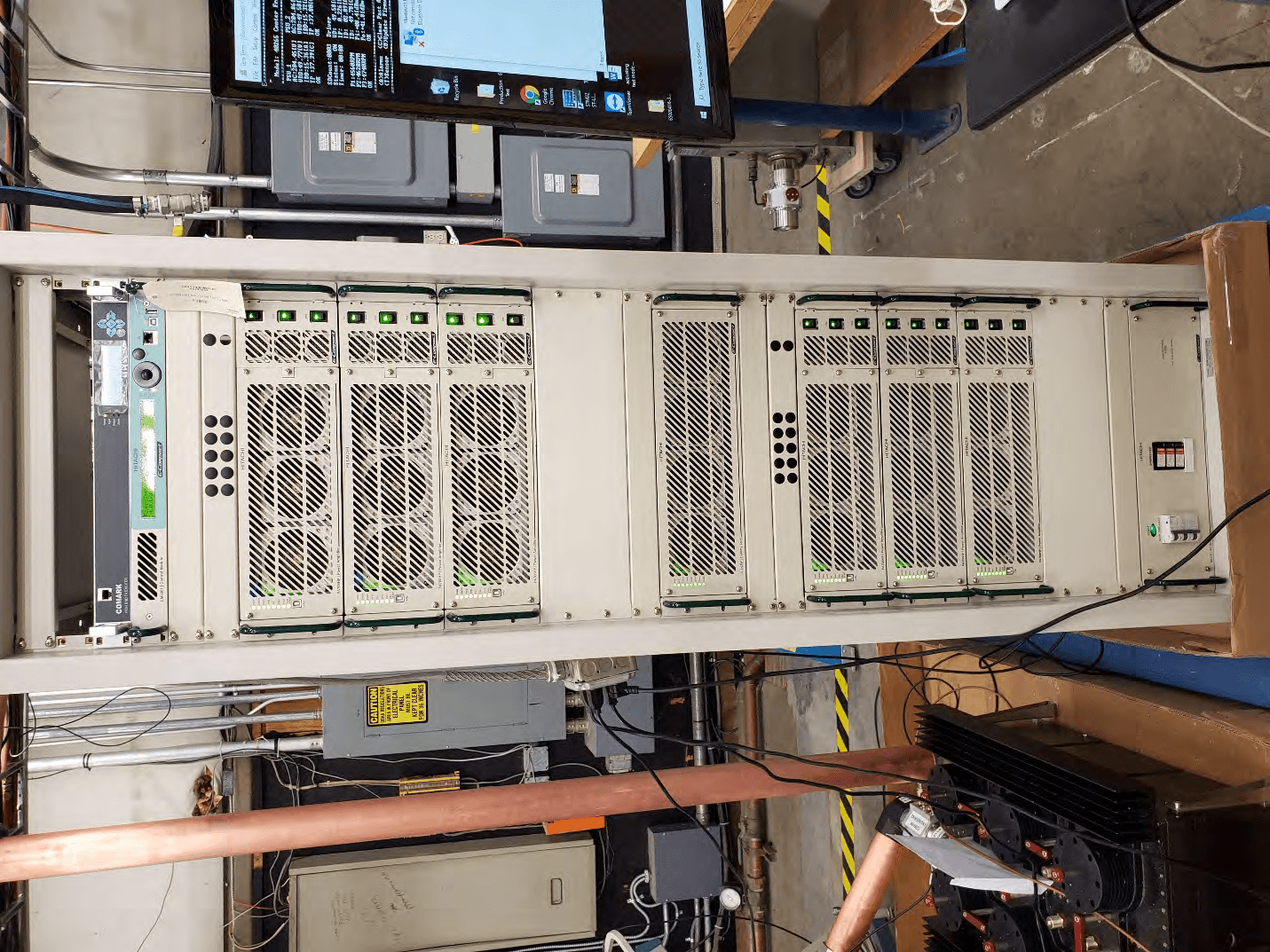
LYIEC706HPBB2
Feb 04, 20216600W/5700W ATSC 1.0/3.0 Transmitter System
Equipment Class
TBC - Licensed Broadcast Station Transmitter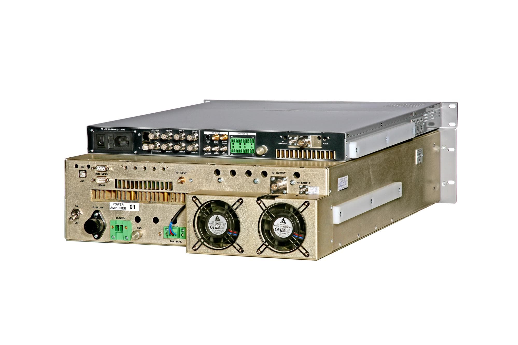
LYIAT1251
Mar 18, 2013250W UHF ATSC Transmitter
Equipment Class
TBC - Licensed Broadcast Station Transmitter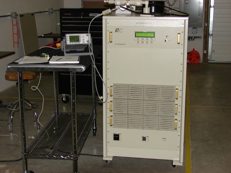
LYIAT7400
Dec 18, 2006400W UHF ATSC Transmitter - Advanced TV
Equipment Class
TBC - Licensed Broadcast Station Transmitter