M6JNL2501LCD Monitor
NPG Display Ltd Taiwan Branch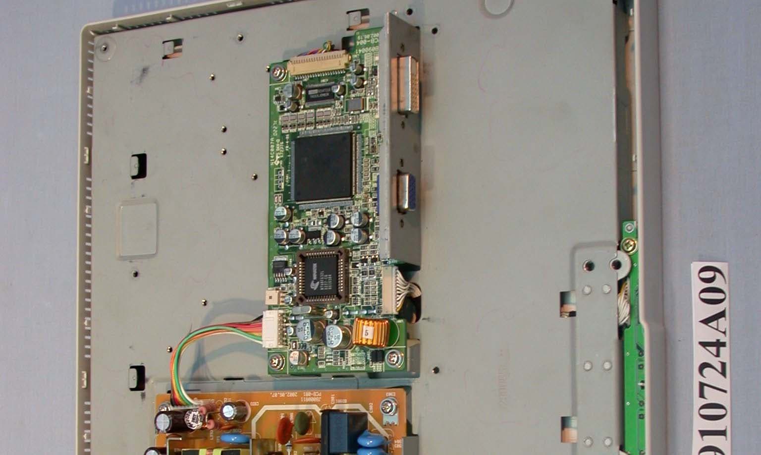
Click to zoom
Application Details
- Equipment Class
- JBP - Part 15 Class B Computing Device Peripheral
- Date of Grant
- Sep 05, 2002
- Application Purpose
- Original Equipment
- Date of Application
- Sep 05, 2002
- Equipment Note
- LCD Monitor
- Country
- Taiwan
Documents & Files
Document Text
Text extracted from the exhibit documents filed with the FCC. Open a document above to read the original.
Users Manual
LCD1501 User’s Manual English English-1 Declaration Declaration of the Manufacturer TO PREVENT FIRE OR SHOCK HAZARDS, DO NOT EXPOSE THIS UNIT TO RAIN OR MOISTURE. ALSO, DO NOT USE THIS UNIT’S POLARIZED PLUG WITH AN EXTENSION CORD RECEPTACLE OR OTHER OUTLETS UNLESS THE PRONGS CAN BE FULLY INSERTED. REFRAIN FROM OPENING THE CABINET AS THERE ARE HIGH VOLTAGE COMPONENTS INSIDE. REFER SERVICING TO QUALIFIED SERVICE PERSONNEL. WARNING CAUTION CAUTION:TO REDUCE THE RISK OF ELECTRIC SHOCK, DO NOT REMOVE COVER (OR BACK). NO USER SERVICEABLE PARTS INSIDE. REFER SERVICING TO QUALIFIED SERVICE PERSONNEL. This symbol warns user that uninsulated voltage within the unit may have sufficient magnitude to cause electric shock. Therefore, it is dangerous to make any kind of contact with any part inside this unit. This symbol alerts the user that important literature concerning the operation and maintenance of this unit has been included. Therefore, it should be read carefully in order to avoid any problems. RISK OF ELECTRIC SHOCK • DO NOT OPEN ENERGY STA R is a U.S. trademark. As an E NERGY STA R ® Partner, NEC-Mitsubishi Electronics Display of America, Inc. has determined that this product meets the ENERGY STA R guidelines for energy efficiency. TheENERGY STA R emblem does not represent EPA endorsement of any product or service. IBM PC/XT/AT, PS/2, MCGA, VGA, 8514/A and XGA are registered trademarks of International Business Machines Corporation. Apple and Macintosh are registered trademarks of Apple Computer Inc. Microsoft and Windows are registered trademarks of the Microsoft Corporation. NEC is a registered trademark of NEC Corporation. All other trademarks or registered trademarks are property of their respective owners. We hereby certify that the colour monitor LCD1501 (NL2502) is in compliance with Council Directive 73/23/EEC: – EN 60950 Council Directive 89/336/EEC: – EN 55022 – EN 61000-3-2 – EN 61000-3-3 – EN 55024 and marked with NEC-Mitsubishi Electric Visual Systems, Corp. MS Shibaura Bldg., 13-23, Shibaura 4-chome, Minato-Ku, Tokyo 108-0023, Japan Caution: When operating the LCD1501 with a 220-240V AC power source in Europe, use the power cord provided with the monitor. In the UK, a BS approved power cord with a moulded plug has a Black (five Amps) fuse installed for use with this equipment. If a power cord is not supplied with this equipment please contact your supplier. When operating the LCD1501 with a 220-240V AC power source in Australia, use the power cord provided with the monitor. For all other cases, use a power cord that matches the AC voltage of the power outlet and has been approved by and complies with the safety standard of your particular country. English English-3 Contents Your new NEC LCD monitor box* should contain the following: •LCD1501 monitor with tilt base •Power Cord •Video Signal Cable •User’s Manual •CD ROM (includes complete User’s Manual in PDF format). To see the User’s Manual, Acrobat Reader 4.0 must be installed on your PC. * Remember to save your original box and packing material to transport or ship the monitor. Quick Start To attach the LCD monitor to your system, follow these instructions: 1. Turn off the power to your computer. 2. Remove cable cover. 3.For PC: Connect the 15-pin mini D-SUB of the appropriate signal cable to the connector for the display card in your system (Figure A.1). Tighten all screws. For Mac: Connect the LCD1501 Macintosh cable adapter to the computer (Figure B.1). Attach the 15-pin mini D-SUB end of the appropriate signal cable to the LCD1501 Macintosh cable adapter (Figure B.1). Tighten all screws. Figure A.1 Figure B.1 Macintosh Cable Adapter (not included) Macintosh G3 and G4 do not need a Macintosh cable adapter 4. Connect the 15-pin mini D-SUB of the video signal cable to the appropriate connector on the back of the monitor (Figure C.1). Place the Video Signal Cable under cable cover. 5. Connect one end of the power cord to the LCD Series monitor and the other end to the power outlet. Place the video signal cable and AC power cord under the cable cover (Figure C.1). Replace cable cover. NOTE:Adjust the position of the cable under the cable cover to avoid damage for cable or monitor. NOTE:Please refer to Caution section of this manual for proper selection of AC power cord. English-4 Figure C.1 Figure D.1 6. The Vacation Switch on the right side of the monitor must be turned on (Figure D.1). Turn on the monitor with the Power Button and the computer. NOTE:The Vacation Switch is a true on/off switch. If this switch is on the OFF position, the monitor cannot be turned on using the front button DO NOT switch on/off repeatedly. 7. No-touch auto adjust automatically adjusts the monitor to optimal settings upon initial setup for most timings. For further adjustments, use the following OSM controls: •Auto Adjust Contrast •Auto Adjust Refer to the Controls section of this User’s Manual for a full description of these OSM controls. NOTE:If you have any problems, please refer to the Troubleshooting section of this User’s Manual. Vacation Switch Power Button Cable Cover English English-5 Tilt Grasp both sides of the monitor screen with your hands and adjust the tilt as desired (Figure TS.1). Remove Monitor Stand for Mounting To prepare the monitor for alternate mounting purposes: 1. Disconnect all cables. 2. Place monitor face down on a non-abrasive surface (Figure R.1). 3. Remove the hinge cover (Figure R.1). 4. Remove the 4 screws connecting the monitor to the stand and lift off the stand assembly (Figure R.2) the monitor is now ready for mounting in an alternate manner. 5. Connect the AC cord and signal cable to the back of the monitor (Figure R.3). 6. Reverse this process to reattach stand. NOTE:Use only VESA-compatible alternative mounting method. Figure TS.1 Figure R.1 Figure R.2 Non-abrasive surface Hinge cover English-6 7. This LCD monitor is designed for use with a flexible arm. Please use the attached screws (4pcs) when mounting. T…
Text truncated - open the document above for the full version.
ID Label/Location Info
(Fig. 1) FCC ID: M6JNL2501 FCC LABEL LOCATION The label will be permanently affixed at a conspicuous location on the device. Label
Internal Photos
(Photo 4) FCC ID:M6JNL2501 (Photo 5) FCC ID:M6JNL2501 (Photo 6) FCC ID:M6JNL2501 (Photo 7) FCC ID:M6JNL2501 (Photo 8) FCC ID:M6JNL2501 (Photo 9) FCC ID:M6JNL2501 (Photo 10) FCC ID:M6JNL2501 (Photo 11) FCC ID:M6JNL2501 2
Internal Photos
(Photo 12) FCC ID:M6JNL2501 (Photo 13) FCC ID:M6JNL2501 (Photo 14) FCC ID:M6JNL2501 (Photo 15) FCC ID:M6JNL2501 (Photo 16) FCC ID:M6JNL2501 (Photo 17) FCC ID:M6JNL2501 (Photo 18) FCC ID:M6JNL2501 (Photo 19) FCC ID:M6JNL2501 (Photo 20) FCC ID:M6JNL2501 1
Schematics
1 1 AA ISSUEDCHECKED KEVIN.WANG DIRECTOR SUFANG.LEE TED.WANG DRAWN FILE NAME: KEVIN.WANG NL2501S-0-3 NL2501/NL2701 KEY SWITCH BOARD 01 NPG DISPLAY LTD. A 11Tuesday, July 23, 2002 Title SizeDocument NumberRev Date:Sheetof LED1 LED2 PWR PLUS MINUS LEFT EXIT NEXT RESET RIGHT GND GND GND SW800KSH06120T 12 J800 52807-1210 1 2 3 4 5 6 7 8 9 10 11 12 1 2 3 4 5 6 7 8 9 10 11 12 SW801KSH06120T 12 SW804KSH06120T 12 SW803KSH06120T 12 D803 1 2 3 SW807KSH06120T 12 SW806KSH06120T 12 SW802KSH06120T 12 SW805KSH06120T 12 5 5 4 4 3 3 2 2 1 1 DD CC BB AA SUFANGTED.WANG KEVIN.WANG NL2501M-0-4 CHECKEDDRAWN KEVIN.WANG ISSUED FILE NAME: DIRECTOR NL2501 MAIN BOARD (DVI_IN) 0-2 NPG DISPLAY LTD. B 16Thursday, June 27, 2002 Title SizeDocument NumberRev Date:Sheetof DVI_B+ DVI_B+ TD2P TDCKN DVI_5V TD0P TD1N DVI_SCLx TD2N TDCKP TD0N TD1P DVI_SDAx DVI_SCL RXC- RX1- RX1+ RX0- RX2+ DVI_DETN RX0+ RXC+ DVI_SDA RX2- 3V3D 3V3D DVI_5V MCU_3_3V R228 10K L211 BLM11P121SGT 12 R219 51*4 1357 2468 R225 4K7 R226 51*4 1357 2468 R220 4K7 J202 DVI CON 1 25 26 1 2 3 4 5 6 7 8 9 10 11 12 13 14 15 16 17 18 19 20 21 22 23 24 C1 C2 C3 C4 C5 C6 25 26 Q202 2SC2412 1 3 2 R227 10K R222 4K7 C213 100N/0805 C209 100P C210 100P R223100 R224100 C211 104P 5 5 4 4 3 3 2 2 1 1 DD CC BB AA 1/10W FILE NAME: DRAWNCHECKED KEVIN.WANGKEVIN.WANG NL2501M-0-4 TED.WANGSUFANG ISSUEDDIRECTOR NL2501 MAIN BOARD (LVDS) 0-2 NPG DISPLAY LTD. B 26Thursday, June 27, 2002 Title SizeDocument NumberRev Date:Sheetof TX0- TX3+ TX2+ TX1+ TXC+ TXC- TX2- TX3- TX1- TX0+ RO0 RO4 BO7 RO1 RO2 RO3 RO5 RO6 RO7 BO0 BO1 BO2 BO3 BO4 BO5 BO6 BO2 BO1 RO4 RO5 GO5 RO0 BO3 GO0 BO5 GO6 GO3 BO7 GO4 BO4 BO6 GO2 RO3 RO7 RO2 GO7 RO1 BO0 GO1 RO6 GO0 GO3 GO4 GO6 GO1 GO7 GO2 GO5 PVCC PVCC PVCC TX0- TX0+ TX1- TX2+ TXC- TX3+ TX1+ TX2- TXC+ TX3- BPCLK BPCLK LVDSPWR PDE PHD PVD RO[0..7](4) GO[0..7] (4) BO[0..7] (4) PANELVCC_CTL1 PVD PCLK4 PDE PHD 3V3D 3V3D 3V3D 3V3D R302 10K +C306 10U/16V 1 2 R301NC 12 C310 103P 0603 1 2 CP306 22P 1357 8642 R3040 12 CP304 22P 1357 8642 CP305 22P 1357 8642 +C308 10U/16V 1 2 C301 104P 1 2 C305104P 1 2 L302 BLM11P121SGT 12 + C309 100U 6.3V 20% 1 2 L301 BLM11P121SGT 12 C315 10P C303 104P 1 2 + C304 10U/16V 1 2 R303 10K 1 2 L304 BLM11P121SGT 1 2 CP301 22P 1357 8642 CP303 22P 1357 8642 C302 104P 1 2 IC301 THC63LVDM83A 51 52 54 55 56 2 3 4 6 7 8 10 11 12 14 15 16 18 19 20 22 23 24 25 27 28 30 5037 38 39 40 41 42 45 46 47 48 33 34 35 36 43 44 49 32 1 9 17 26 5 13 31 21 29 53 TXIN0 TXIN1 TXIN2 TXIN3 TXIN4 TXIN5 TXIN6 TXIN7 TXIN8 TXIN9 TXIN10 TXIN11 TXIN12 TXIN13 TXIN14 TXIN15 TXIN16 TXIN17 TXIN18 TXIN19 TXIN20 TXIN21 TXIN22 TXIN23 TXIN24 TXIN25 TXIN26 TXIN27TXOUT3+ TXOUT3- TXCLKOUT+ TXCLKOUT- TXOUT2+ TXOUT2- TXOUT1+ TXOUT1- TXOUT0+ TXOUT0- PLLGND1 PLLVCC PLLGND LVDSGND2 LVDSGND1 LVDSVCC LVDSGND PWRDWN VCC3 VCC2 VCC1 VCC GND4 GND3 TXCLKIN GND2 GND1 GND C313 10P C307 104P 1 2 CP302 22P 1357 8642 +C311 10U/16V 1 2 J301 DF14A-20P-1.25H_21 1 2 3 4 5 6 7 8 9 10 11 12 13 14 15 16 17 18 19 20 1 2 3 4 5 6 7 8 9 10 11 12 13 14 15 16 17 18 19 20 C312 22P G D S IC302 HAT1053M 521 4 6 3 L303 BLM11P121SGT 12 C314 10P Q301 DTC144WK 3 1 2 5 5 4 4 3 3 2 2 1 1 DD CC BB AA FILE NAME: KEVIN.WANGKEVIN.WANG NL2501M-0-4 TED.WANGSUFANG NL2501 MAIN BOARD (MCU) NPG DISPLAY LTD. 1 2 12 12 1 2 1 2 12 12 12 12 1 32 12 12 1 2 1 2 3 4 5 6 7 8 1 2 1 2 12 12 1 2 3 4 5 6 7 8 9 10 11 12 1 2 3 4 5 6 7 8 9 10 11 12 1 32 1 2 1 2 1 2 1 2 1 2 1 2 1 2 1 2 12 12 1 2 1 2 3 45 6 7 8 PRE E1 E2 VSSSDA SCL /WC VCC 12 1 2 NT68F632L 123456 7 8 9 10 11 12 13 14 15 16 17 1819202122232425262728 29 30 31 32 33 34 35 36 37 38 39 4041424344 PC2/SOG1 PC1PC0 RSTB VCC PD6 GND OSC0 OSC1 P30/RX P31/TX P34/T0 P35/T1 PB3/AD3/INT1 PB2/AD2/INT0 PB1/AD1 PB0/AD0 PA7/PWM9PA6/PWM8PA5/PWM7PA4/PWM6PA3/PWM5PA2/PWM4PA1PWM3PB7/SDA1PB6/SCL1PB5/SDA0PB4/SCL0 PA0/PWM2 PD5/CLP0 PD4/HALF1 PD3/HALF0 PD2/VSYNC0 PD1/HSYNC0 PD0 PC7 PC6 PE0 PE1 PC5/PATT0PC4/PWM1PC3/PWM0 HSYNC1VSYNC1 12 3 1 2 12 12 1 2 3 4 12 12 34 56 78 12 1 2 12 12 12 1 2 12 1 2 3 4 5 6 7 8 12 12 12 5 5 4 4 3 3 2 2 1 1 DD CC BB AA POWER SWITCH 1/10W1/10W FILE NAME: DRAWNCHECKED KEVIN.WANGKEVIN.WANG NL2501M-0-4 TED.WANGSUFANG ISSUEDDIRECTOR NL2501 MAIN BOARD (POWER) 0-2 NPG DISPLAY LTD. B 46Thursday, June 27, 2002 Title SizeDocument NumberRev Date:Sheetof PWR_EN +3_3V Vref +3_3V Vref Vref Vref +3_3V PWR_EN TP_PWR TP_PWR BACKLIG_ON_OFF1 PWR_SW1 BRIGHTNESS4 TP_CTL 12VIN +5VP +5VP +5VP +5VP 12VIN 12VIN 12VIN 5VD 3V3D 12VIN +5VP +C602 470U 25V 1 2 D601 1SS355 12 R617 1K 1 2 D602 SSM24 1 2 C6081U 12 R615 10K 12 Q603 2SC2412 1 3 2 C624 104P +C617 NC 1 2 R613 5K1 1 2 C625 104P R6083K6 12 Q601 2SC2412 1 3 2 R601 4K7 1 2 R606 510 1 2 PQ05DZ5 1 IC604 PQ05DZ51 1 2 3 4 5 Vin CTL O/P NC GND C615 103P 1 2 C618 102P 1 2 AP494A IC601 AP494A 1 2 3 4 5 6 7 8 9 10 11 12 13 14 15 16 IN1+ IN1- FB DTC CT RT GND C1 E1 E2 C2 VCC O/P CTL REF IN2- IN2+ FD1 FIDUCIAL-MARK 1 R628 1.96K 1 2 + C613 100U 16V 1 2 FD2 FIDUCIAL-MARK 1 C611 104P FD3 FIDUCIAL-MARK 1 FD4 FIDUCIAL-MARK 1 R61110K 12 MTG1 MTG/ID1.2/OD2 1 IC605 BD4743G 1 2 34 5 NC SUB GNDVout Vin J602 53015-0210 1 2 1 2 C606102P 12 R607 10 1 2 MTG2 MTG/ID1.2/OD2 1 C616 103P 1 2 C603 223P 1 2 MTG3 MTG/ID1.2/OD2 1 C619 103P 1 2 MTG4 MTG/ID1.2/OD2 1 + C614 470U 25V 1 2 +C609 10U/16V 1 2 L603 BLM11P121SGT 12 R623 4K7 1 2 D603 RLZ5.6C 12 C600 1U 1 2 C621 103P 1 2 C622 103P 1 2 R618 4K7 1 2 L604 BLM11P121SGT 1 2 R620 470 R624 470 C623 103P 1 2 R625220 12 R605 1K 1% 1 2 R602 1K 1 2 L602 BLM11P121SGT 12 R609 120K 1 2 R604 0 1 2 IC603A 74F74 SO14 2 3 5 6 14 4 7 1 D CLK Q Q VCC PR GND CL Q604 DTC114WK 3 1 2 G D S IC602 SI3457DV 521 4 6 3 R626220 12 + C612 10U/16V 1 2 R6270 12 C607 102P 1 2 R619 470 J601 PWR-7P 1 2 3 4 5 6 7 R610 1M 1 2 R603 0 1 2 R622 1K +C620 NC 1 2 C610 10u/16V D605 SSM24 1 2 F601 1.8A/50V 12 C601 103P 1 2 R6211K R616 10K 1 2 MTG5 MTG/ID1.2/OD2 1 L601 33UH 12 D604 MMBZ5331 1 2 Q602 2SA1037 1 3 2 5 5 4 4 3 3 2 2 1 1 DD CC BB AA as close as possible the scaler chip FILE NAME: DRAWNCHECKED KEVIN.WANGKEVIN.WANG NL2501M-0-4 TED.WANGSUFANG ISSUEDDIRECTOR NL2501 MA…
Text truncated - open the document above for the full version.
Test Report
FCC ID: M6JNL2501 Report No.: F910724A091Issued: August 7, 2002 FCC TEST REPORT REPORT NO.: F910724A09 MODEL NO.: NL2501 RECEIVED: July 24, 2002 TESTED: August 2, 2002 APPLICANT: NPG Display LTD., Taiwan Branch ADDRESS: 2FL-1, No. 8, Tunhua N. Rd., Taipei, Taiwan, R.O.C. ISSUED BY: Advance Data Technology Corporation LAB LOCATION: 47 14th Lin, Chiapau Tsun, Linko, Taipei, Taiwan, R.O.C. This test report consists of 24 pages in total. It may be duplicated completely for legal use with the approval of the applicant. It should not be reproduced except in full, without the written approval of our laboratory. The client should not use it to claim product endorsement by CNLA, NVLAP or any government agencies. The test results in the report only apply to the tested sample. The test results in this report are traceable to the national or international standards. 0528 ILAC MRA Lab Code: 200102-0 FCC ID: M6JNL2501 Report No.: F910724A092Issued: August 7, 2002 Table of Contents 1CERTIFICATION............................................................................................. 3 2SUMMARY OF TEST RESULTS .................................................................... 4 3GENERAL INFORMATION ............................................................................. 5 3.1GENERAL DESCRIPTION OF EUT ................................................................5 3.2DESCRIPTION OF TEST MODES ..................................................................5 3.3DESCRIPTION OF SUPPORT UNITS ............................................................6 4EMISSION TEST ............................................................................................ 7 4.1CONDUCTED EMISSION MEASUREMENT...................................................7 4.1.1 LIMITS OF CONDUCTED EMISSION MEASUREMENT ................................7 4.1.2 TEST INSTRUMENTS.....................................................................................7 4.1.3 TEST PROCEDURE........................................................................................8 4.1.4 DEVIATION FROM TEST STANDARD............................................................8 4.1.5 TEST SETUP...................................................................................................8 4.1.6 EUT OPERATING CONDITIONS ....................................................................9 4.1.7 TEST RESULTS (A).......................................................................................10 4.1.8 TEST RESULTS (B).......................................................................................12 4.2RADIATED EMISSION MEASUREMENT......................................................14 4.2.1 LIMITS OF RADIATED EMISSION MEASUREMENT ...................................14 4.2.2 TEST INSTRUMENTS...................................................................................15 4.2.3 TEST PROCEDURE......................................................................................15 4.2.4 DEVIATION FROM TEST STANDARD..........................................................16 4.2.5 TEST SETUP.................................................................................................17 4.2.6 EUT OPERATING CONDITIONS ..................................................................17 4.2.7 TEST RESULTS (A).......................................................................................18 4.2.8 TEST RESULTS (B).......................................................................................20 5PHOTOGRAPHS OF THE TEST CONFIGURATION ................................... 22 6APPENDIX - INFORMATION ON THE TESTING LABORATORIES ............ 24 FCC ID: M6JNL2501 Report No.: F910724A093Issued: August 7, 2002 1 CERTIFICATION PRODUCT:15” LCD Monitor BRAND NAME:NEC, Mitsubishi MODEL NO:NL2501 TEST ITEM:ENGINEERING SAMPLE APPLICANT:NPG Display LTD., Taiwan Branch STANDARDS:FCC Part 15, Subpart B, Class B CISPR 22: 1997, Class B ANSI C63.4-1992 We, Advance Data Technology Corporation, hereby certify that one sample of the designation has been tested in our facility on July 29, 2002. The test record, data evaluation and Equipment Under Test (EUT) configurations represented herein are true and accurate accounts of the measurements of the sample's EMC characteristics under the conditions herein specified. CHECKED BY: , DATE:August 7, 2002 ( Emily Lai ) APPROVED BY:, DATE:August 7, 2002 (Fred Chen/ Manager ) FCC ID: M6JNL2501 Report No.: F910724A094Issued: August 7, 2002 2 SUMMARY OF TEST RESULTS The EUT has been tested according to the following specifications: StandardTest TypeResultRemarks Conducted TestPASS Meets Class B Limit Minimum passing margin is –8.42 dB at 0.271 MHz FCC Part 15, Subpart B, Class B / CISPR 22: 1997, Class B Radiated TestPASS Meets Class B Limit Minimum passing margin is –3.30 dB at 910.00 MHz NOTE: For conducted emission test, the test limit used is according to FCC Part 15.107. In this part, conducted emission test for telecom port is not mentioned and therefore this item is not tested. FCC ID: M6JNL2501 Report No.: F910724A095Issued: August 7, 2002 3 GENERAL INFORMATION 3.1 GENERAL DESCRIPTION OF EUT PRODUCT 15” LCD Monitor MODEL NO. NL2501 POWER SUPPLY Switching Power Cord: Nonshielded, 3 pin, AC (1.8m) DATA CABLE Shielded DVI cable (1.8m) with two ferrite cores Shielded D-SUB cable (1.8m) with two ferrite cores NOTE: The EUT is a 15” LCD Monitor with resolution up to 1024x768. For a more detailed features description, please refer to the manufacturer's specifications or the User's Manual. 3.2 DESCRIPTION OF TEST MODES The EUT was pre-tested under the following conditions in electromagnetic interference: CONDITIONCONFIGURATION 11024X768 (60kHz) 2800x600 (48kHz) 3640x480 (31kHz) Since the worst emission levels were found when the EUT was tested under 1024X768 (60kHz) resolution, both DVI and D-Sub Mode. So Condition 1 is adopted for the final test. FCC ID: M6JNL2501 Report No.: F910724A096Issued: Au…
Text truncated - open the document above for the full version.
Test Setup Photos
FCC ID: M6JNL2501 Report No.: F910724A0922Issued: August 7, 2002 5 PHOTOGRAPHS OF THE TEST CONFIGURATION CONDUCTED EMISSION TEST FCC ID: M6JNL2501 Report No.: F910724A0923Issued: August 7, 2002 RADIATED EMISSION TEST
Contact Information
Applicant
Yasuhisa Okano(General Manager)
886 2 703-8262Fax: 886 2 702-9472
Test Firm
Bureau Veritas CPS (H.K.) Ltd. Taoyuan BranchTommy Wu
Technical Specifications
| # | Rule Parts | Frequency Range | Power Output |
|---|---|---|---|
| 1 | 15B | - | - |
Other Applications from NPG Display Ltd Taiwan Branch
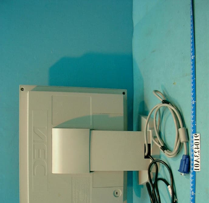
M6JNL1503
May 16, 2002LCD Monitor
Equipment Class
JBP - Part 15 Class B Computing Device Peripheral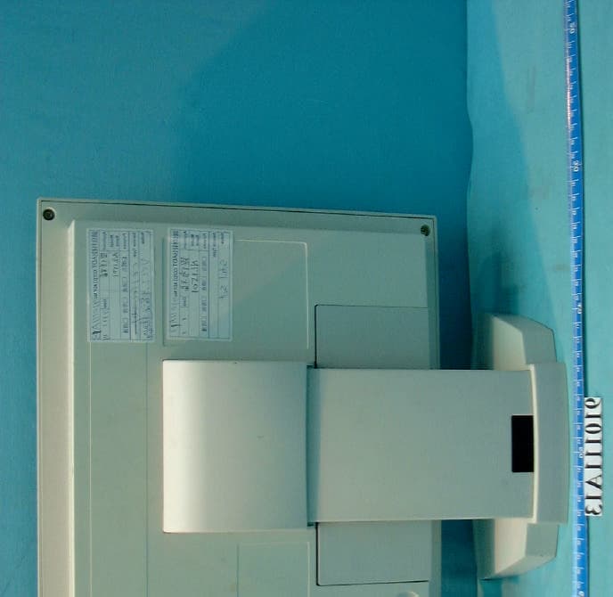
M6JNL1501
Feb 06, 2002LCD Monitor
Equipment Class
JBP - Part 15 Class B Computing Device Peripheral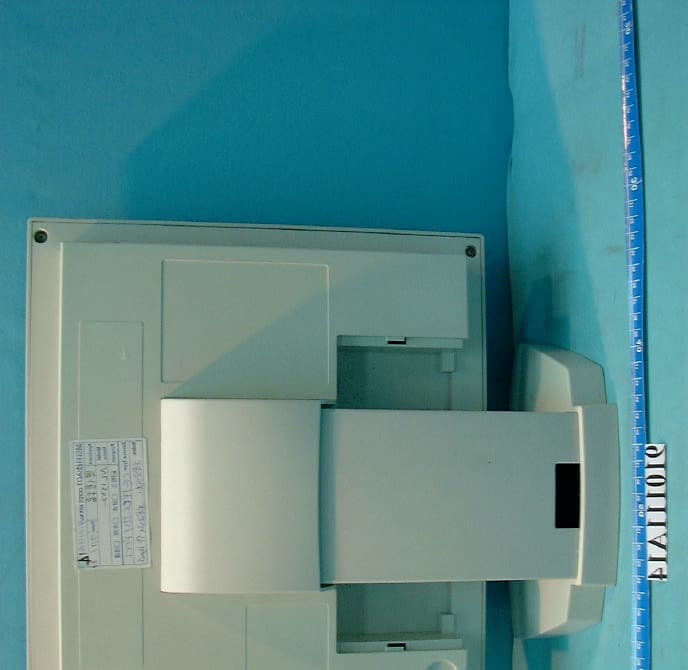
M6JNL1502
Jan 29, 2002LCD Monitor
Equipment Class
JBP - Part 15 Class B Computing Device Peripheral
M6JN0706
Jun 18, 2001Color Monitor
Equipment Class
JBP - Part 15 Class B Computing Device Peripheral
M6JN0902
Jun 18, 2001Color Monitor
Equipment Class
JBP - Part 15 Class B Computing Device Peripheral