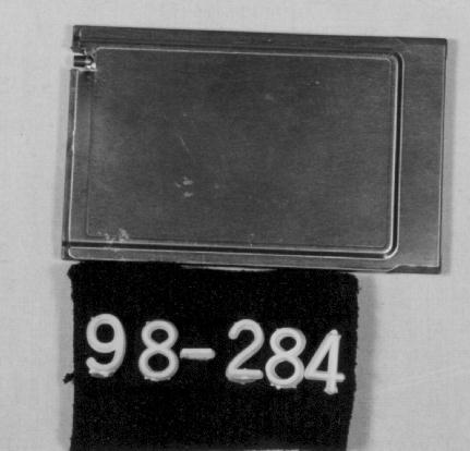
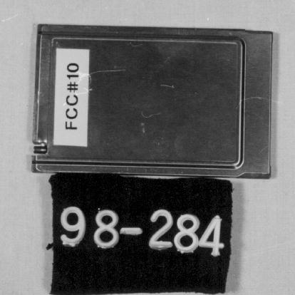
MIVWG9701ACDPD/AMPS PCMCIA Wireless Modem
Novatel Wireless Inc.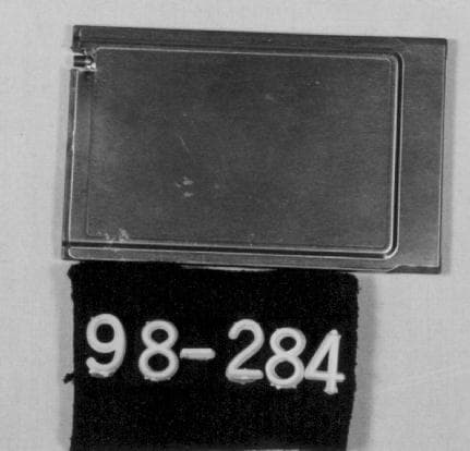
Click to zoom
Application Details
- Equipment Class
- TNB - Licensed Non-Broadcast Station Transmitter
- Date of Grant
- Nov 19, 1998
- Application Purpose
- Original Equipment
- Date of Application
- Jun 09, 1998
- Equipment Note
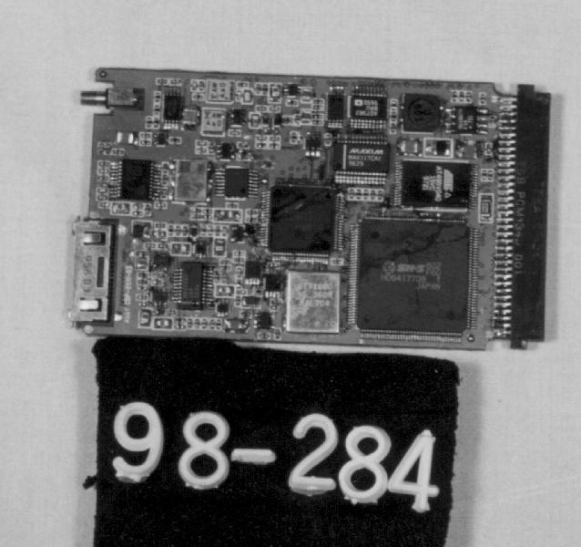
- CDPD/AMPS PCMCIA Wireless Modem
- Frequency Range
- 824.01000000 - 848.01000000
- Company
- Novatel Wireless Inc.
- Country
- Canada
Documents & Files

Document Text
Text extracted from the exhibit documents filed with the FCC. Open a document above to read the original.
Attestation Statements
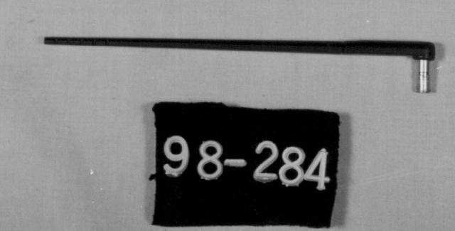
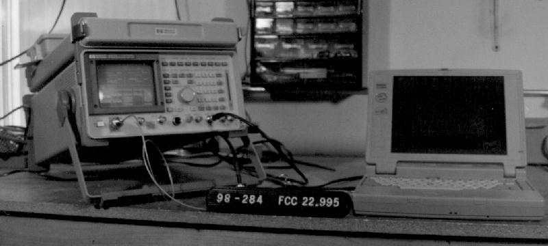
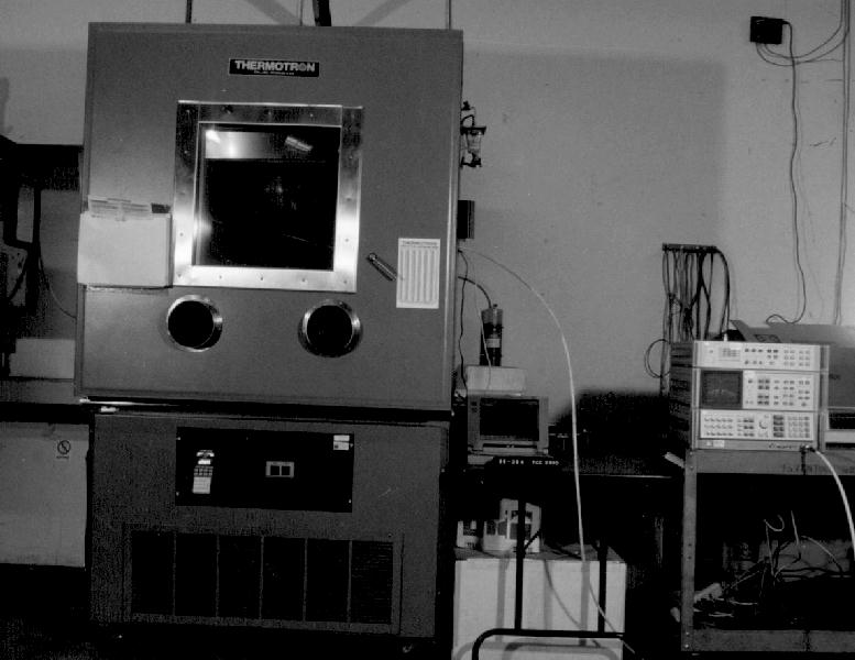
1 REPLY TO REQUEST FOR ADDITIONAL INFORMATION INET SPIDER II MODEM FCC ID MIVWG9701A August 19, 1998 This document has been compiled to reply to a series of questions posed by the FCC as part of the Equipment Authorization Process for the Inet Spider II Modem (FCC ID MIVWG9701A). Each of the questions listed by the FCC Is listed prior to the reply. 1) Please indicate whether and how a specific antenna assembly will always be used with this unit. Note that the antenna will affect the ERP and SAR results. Answer The Spider II will be marketed and sold with the 1/2-wave dipole antenna it was tested with. The absolute most power that can theoretically be transmitted from the unit by design is 28 dBm. There are no antennas on the market today that will attach directly to the unit other than the one tested. The antenna and the PCMCIA transmitter use a subminiature SMC type connector set which is not available as an accessory on the open (accessable by the standard consumer) market. There are a set of follow-on products which are in development at this time, but any items which can affect the radiated power of the device will be tested and submitted for authorization in accordance with Commission regulations. 2) SAR report not received by the Commission Answer SAR report was retransmitted to the Commission during the week of August 10, 1998 3) Please explain why for conducted power output (Pages 15 and 16) the AMPS mode mode is higher while for the ERP the CDPD mode is higher (Page 21). Answer In the case of the conducted power output data, the AMPS mode was reading an average of 1.4 dB higher than the CDPD mode. For ERP, the CDPD mode was reading an average of 2.0 dB higher than the AMPS readings. While both operational modes use the same basic RF sections (giving the same basic transmit power capability) the CDPD signal is spread/distributed differently than the AMPS signal. For the conducted power data, the reported data was derived from the occupied bandwidth plots which were made using a 300Hz/300Hz bandwidth setting. The ERP data was obtained using 100kHz/300kHz bandwidth settings. Based on tests performed on similar products, a 2 shift in relative power can occur between operating modes based on measurement bandwidth. Usually, this shift is 2 to 3 dB, which is on the order of the shift seen here. 4) Please send an occupied bandwidth plot for operation in the wideband data mode. Answer Data for the wideband data operation in AMPS mode is included with this reply. Data is also present for operation in wideband mode for signalling tone plus SAT . Data is presented for three channels across the band. 5) Please send measurement data showing modulation limiting (for voice operation). Answer Modulation limiting was performed using the following procedure: "Perform this test on channel 365. Setup includes compressor enabled and SAT disabled. Input an audio signal at 1 KHz at a level to produce +/-8KHz deviation. Increase level by 20 dB (rise time <0.1 ms)." Test was performed using an HP 8920A test set with the following results: Peak Deviation measured = 11.9 KHz spec = 12 KHz Steady-State Deviation measured = 11.8 KHz spec = 12 KHz 6) Please sned measurement data showing compliance with the audio low pass filter specifications in Section 22.915(d)(1) of the Commissions R&R. Answer The low pass filter data is in paragraph 5.0 and Appendix D of the test report. 7) Your frequency stability rating of 0.0005% does not satisfy the requirement under Section 22.335 of the Commissions R&R. Answer The latest edition of 47 CFR owned by PTI is the October 1996 edition. Section 22.355 of this document quotes the frequency tolerance as being contained in Table C-1 of Scetion 22.357. While Section 22.357 references §22.359 and §22.917, there appears to be no Table C-1 in this edition of Section 22. The figure quoted in the 731 was derived from a similar application. After doing some additional research, it appears that the frequency stability requirement as I understand it is 2.5 ppm. The Spider II easily meets this requirement. The frequency 3 stability data for the Spider II indicates that this unit eaily meets the 2.5 ppm criteria. Assuming that 2.5 ppm is the correct rating, please correct the Form 731 to this figure. 4 OCCUPIED BANDWIDTH DATA SHEET INET SPIDER II WIRELESS MODEM FCC ID MIVWG9701A Sample: FCC #08 Test Date: August 12, 1998Port: Antenna I/O Mode: Wideband DataChannel: 367 COMMENT: Center Frequency = 836.01 MHz 5 OCCUPIED BANDWIDTH DATA SHEET INET SPIDER II WIRELESS MODEM FCC ID MIVWG9701A Sample: FCC #08 Test Date: August 12, 1998Port: Antenna I/O Mode: Wideband Signal with SAT toneChannel: 367 COMMENT: Center Frequency = 836.01 MHz 6 OCCUPIED BANDWIDTH DATA SHEET INET SPIDER II WIRELESS MODEM FCC ID MIVWG9701A Sample: FCC #08 Test Date: August 12, 1998Port: Antenna I/O Mode: Wideband DataChannel: 799 COMMENT: Center Frequency = 848.97 MHz 7 OCCUPIED BANDWIDTH DATA SHEET INET SPIDER II WIRELESS MODEM FCC ID MIVWG9701A Sample: FCC #08 Test Date: August 12, 1998Port: Antenna I/O Mode: Wideband DataChannel: 799 COMMENT: Center Frequency = = 848.97 MHz 8 OCCUPIED BANDWIDTH DATA SHEET INET SPIDER II WIRELESS MODEM FCC ID MIVWG9701A Sample: FCC #08 Test Date: August 12, 1998Port: Antenna I/O Mode: Wideband DataChannel: 991 COMMENT: Center Frequency = 824.04 MHz 9 OCCUPIED BANDWIDTH DATA SHEET INET SPIDER II WIRELESS MODEM FCC ID MIVWG9701A Sample: FCC #08 Test Date: August 12, 1998Port: Antenna I/O Mode: Wideband DataChannel: 991 COMMENT: Center Frequency = = 824.04 MHz
ID Label/Location Info
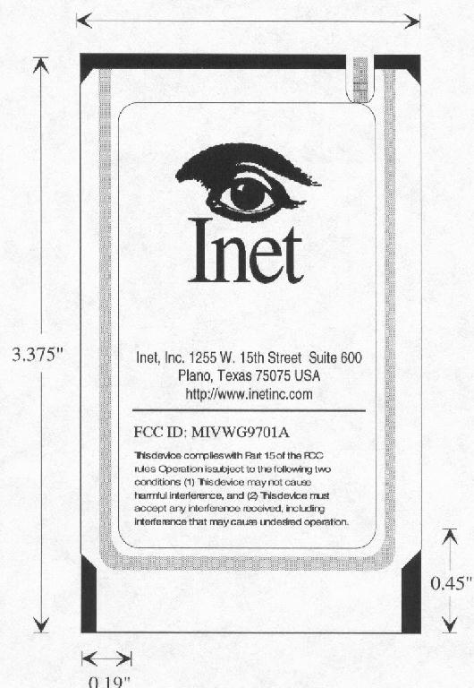
June 16, 1998 Federal Communications Commission Equipment Authorization Division, Application Processing Branch 7435 Oakland Mills Road Columbia, Maryland 21046 Subject: Model Name Change: FCC ID MIVGW9701A To Whom It May Concern: The model name for the item idenfied under FCC ID MIVWG9701A should be changed in all instances for the subject application as listed below: Old Listing:Inet Inc., SPIDER MITE PCMCIA CDPD/CS Modem New Listing:Inet Inc., SPIDER II PCMCIA CDPD/CS Modem This change should be made to the Form 731, Reports and Label information. If you have any questions during your review, please contact me. Sincerely, Jeffrey A. Lenk President Professional Testing (EMI) Inc. Round Rock, Texas cc:John F. O’Brien, Senior Engineer Professional Testing (EMI) Inc.
Operational Description
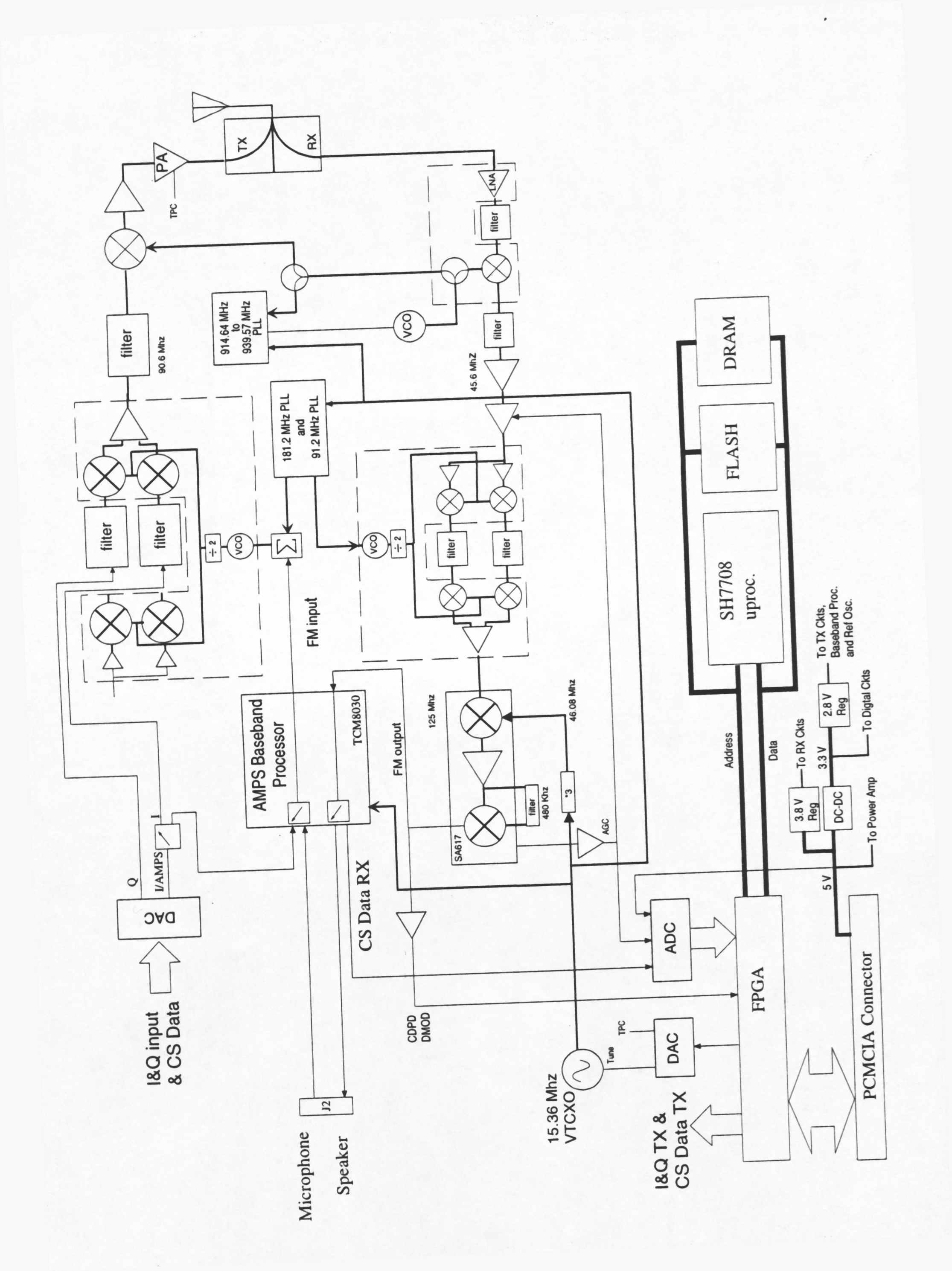
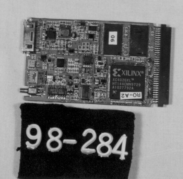
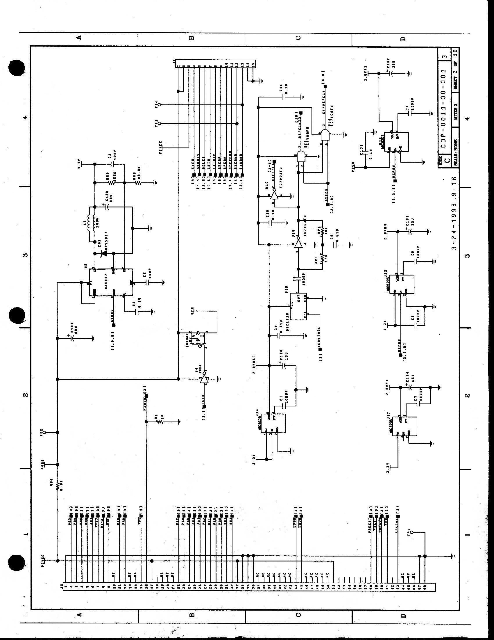
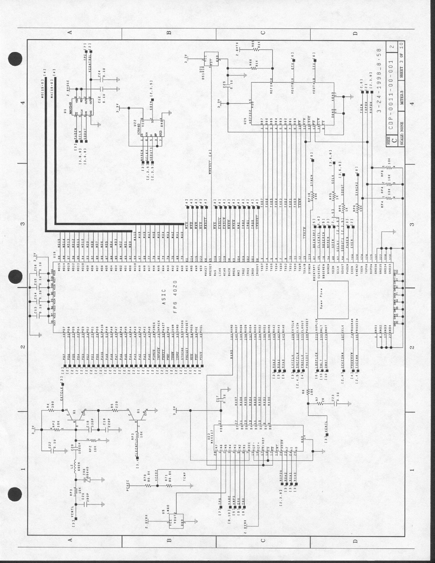
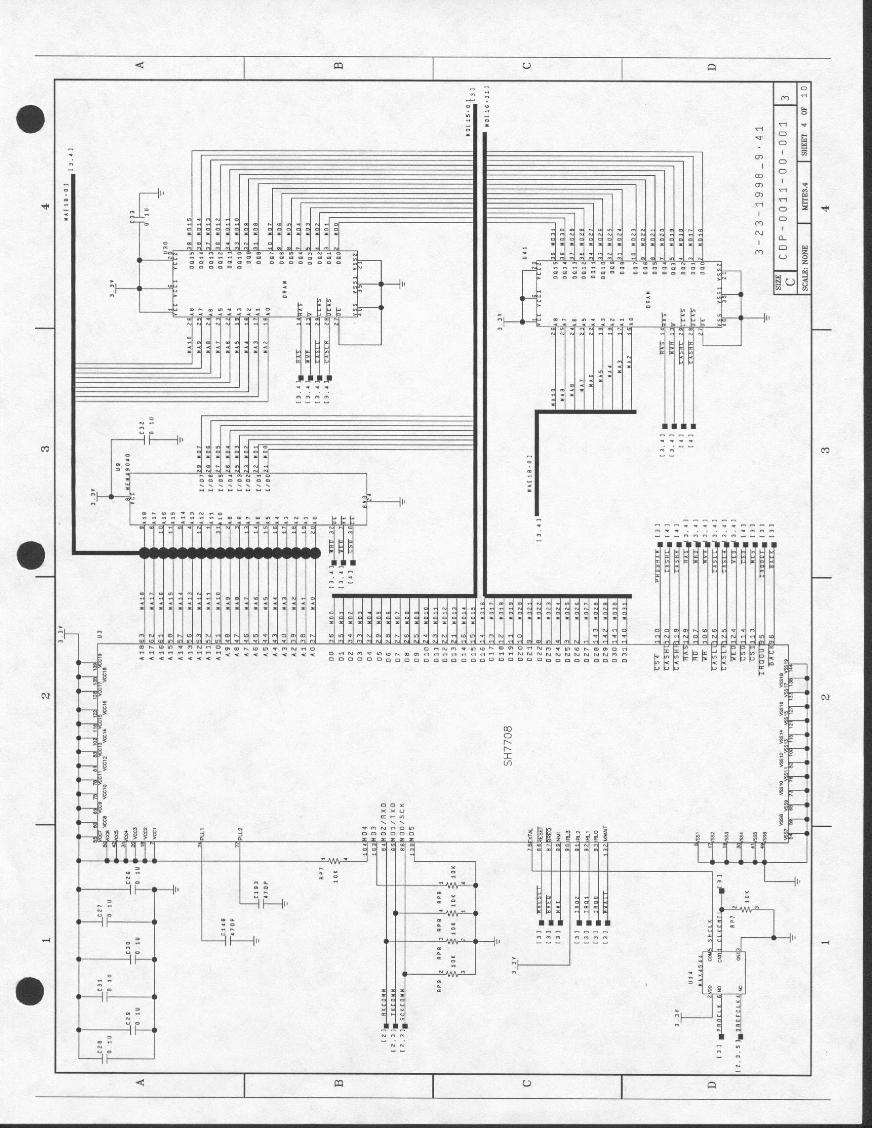
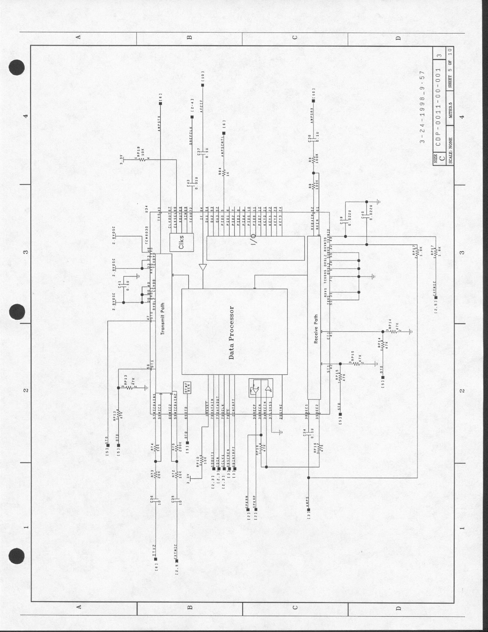
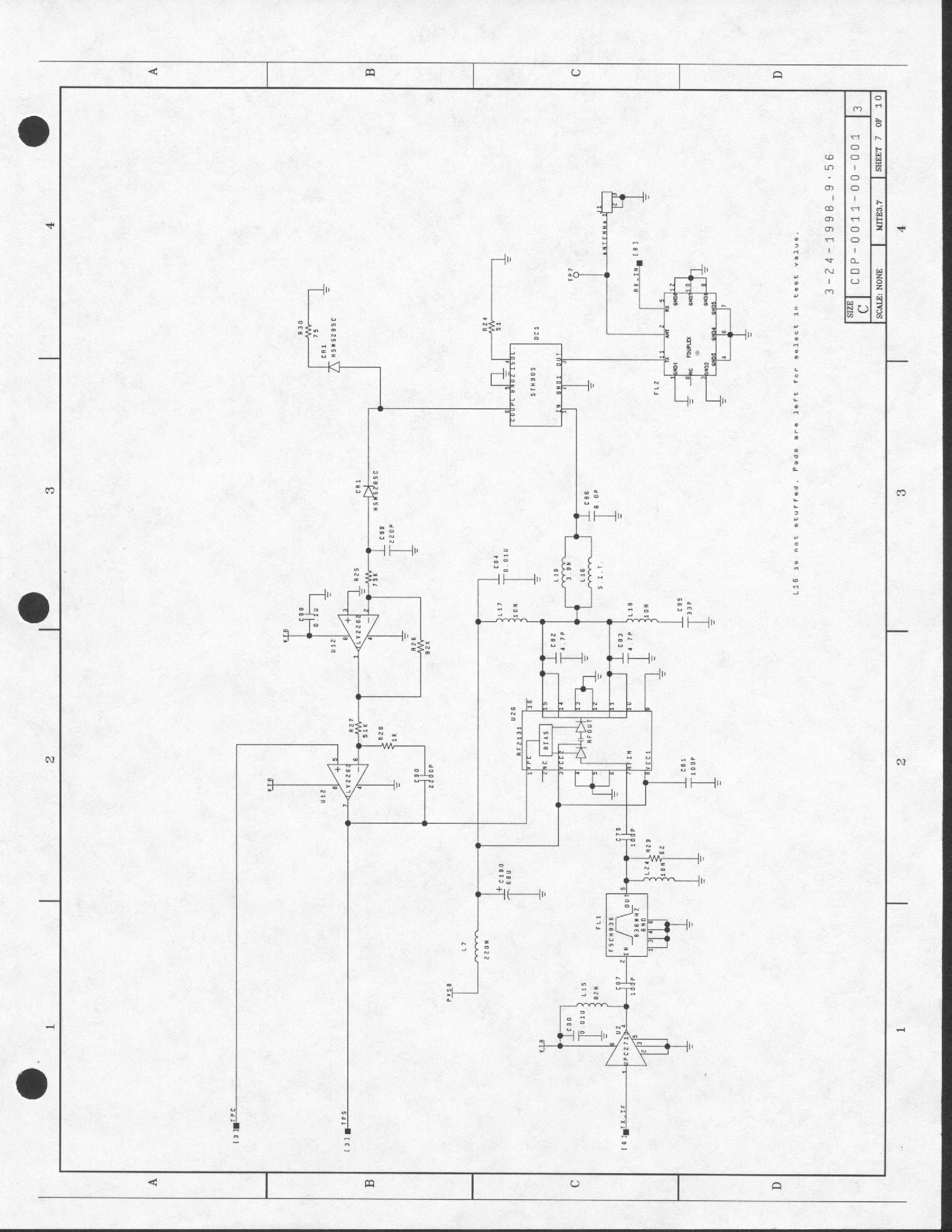
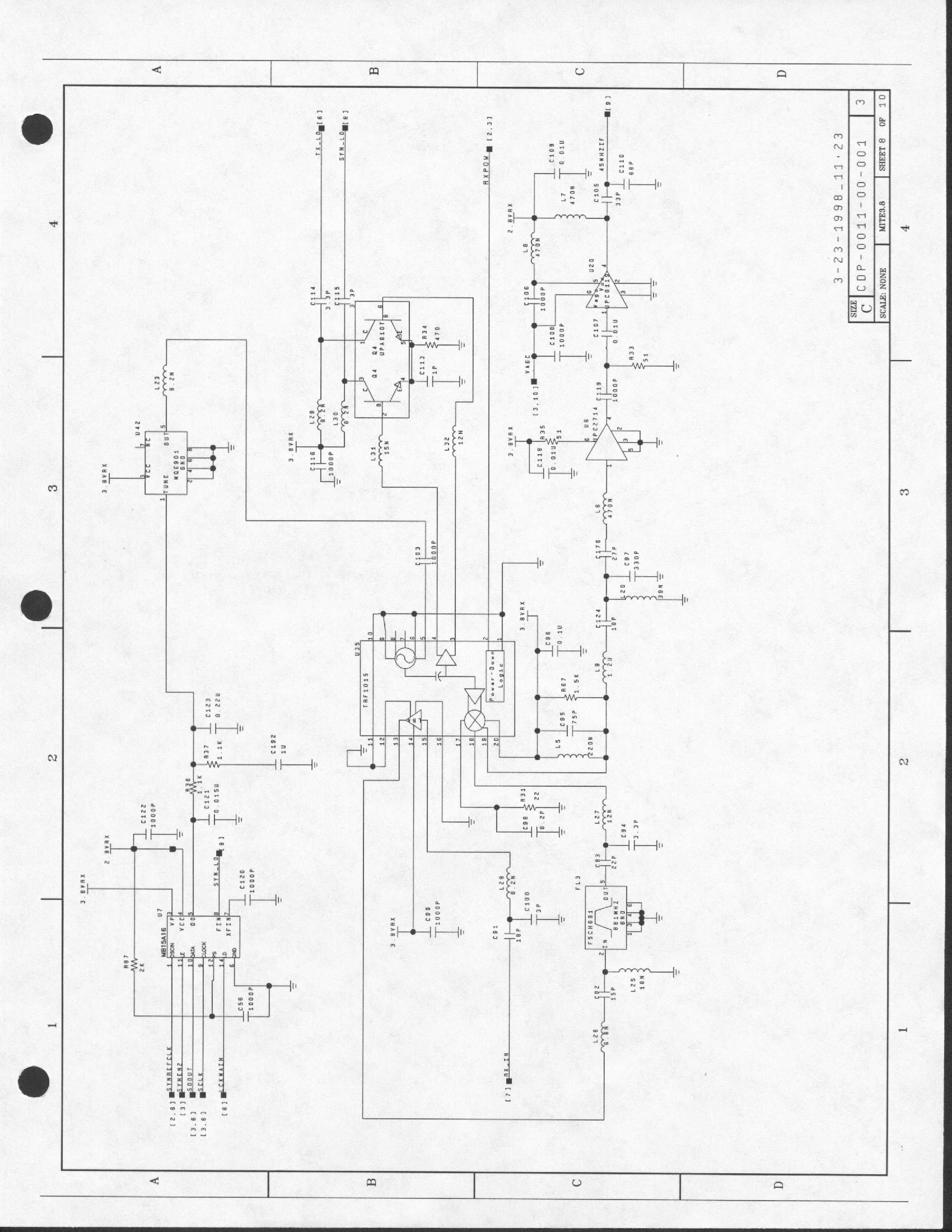
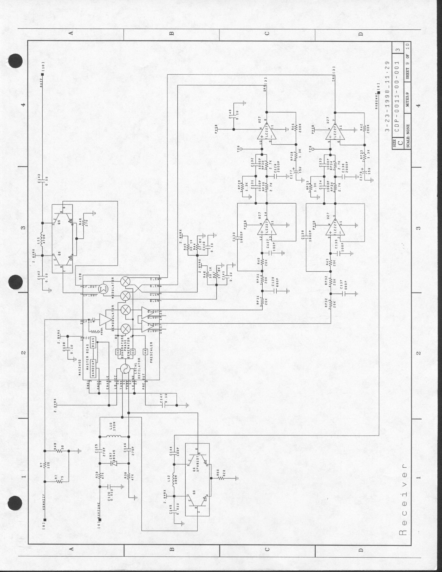
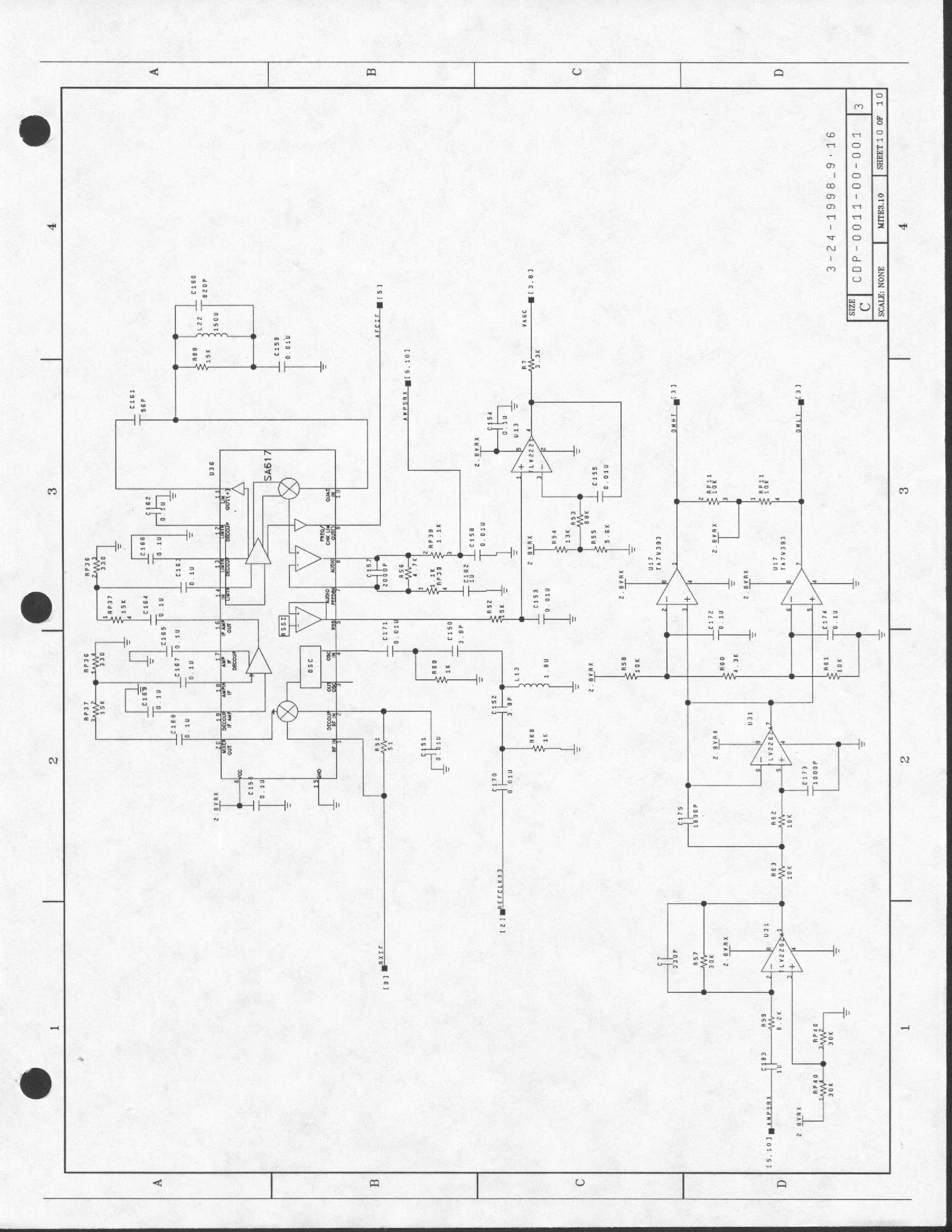
INET Spider II CDPD/CS Modem Technical Summary The INET Spider II product is a CDPD and Circuit Switched cellular modem designed to be compliant with Cellular Digital Packet Data System Specification - Release 1.1 and the Mobile Station - Land Station Compatibility Specification - EIAITIA-553. The modem is a completely self contained unit consisting of a processor and memory for data packetizeing, encryption, encoding, decryption, and decoding. It contains all of the RF transmit and receive circuitry required for AMPS call processing as well as creating and receiving a CDPD data stream on any standard cellular channel. The technology used in the construction of the modem mimics that of an AMPS cellular phone with its wideband data and voice capabilities. In addition, the modem has provisions for performing GMSK data bursts. The product is packaged in a PCMCIA Type II housing and is solely powered and controlled through a PCMCIA PC Card version 2.1 interface. This interface specifies the DC voltage to be provided to the PCMCIA peripheral as a regulated 5 volts +A5%. The interface protocol is design to emulated a standard 16550 UART interface and can be configured on the PC side as a standard Communication Port connection. The data flow into and out of the modem is metered by the modem processor. The data rate of transmission at the antenna terminal is fixed at 19.2 KHz in CDPD mode and 14.4 KHz in circuit switched/AMPS modem mode and is independent of any user application running on the PC side. The modem processor takes care of implementing all protocol controls on the CDPD channel and the aspects of the CDPD channel are not apparent to the users application. The protocol controls in AMPS mode are handled by the processor in conjunction with a TCM8O3O Baseband Processor for Analog Cellular Telephones. Transmitter frequency and emissions type. The transmitter covers the band of 824.010 MHz to 848.970 MHz and is tuned in 30 KHz steps. In CDPD mode, the modulation type is a Gaussian Minimum Shift Keying (GMSK) with BT= .5. The data rate is fixed at 19.2 Kbps. In the AMPS Circuit Switched mode, the modulation type is FSK with a data rate of 14.4 Kbps. Modulation of a carrier is done at the Transmit LO (181.2 MHz) with an I and Q modulator in CDPD mode and a standard FM modulator in AMPS mode. The baseband I and Q waveforms and the FM waveforms, with all of the filter characteristics required to meet the emissions mask, have been described digitally and stored permanently in non-volatile memory. A microcontroller is used to translate the data stream to be transmitted into the appropriate baseband signals. The digital signals are generated at 16 times over sampling, and the analog signals are recreated with an 8-bit digital-to- analog conversion process. This modulation technique requires no tuning or adjustments to meet the emissions mask. Also, because the data is encoded with a pseudo random sequence, the modulation mask is constant and independent of the data being sent. The output spectrum is constant and independent of user controls except for on/off commands. The emissions mask as detailed in the CDPD version 1.1 system specification is: the emission power in either adjacent channel centered +1-30 KHz from the center frequency shall not exceed a level of 26 dB below the mean output power. The emission power in either alternate channel, centered +1-60 KHz from the center frequency shall not exceed a power level of 45 dB below the mean output power. The emission power in either second alternate channel centered +1-90 KHz from the center frequency shall not exceed a power level of 60 dB below the mean output power or -23 dBm, whichever is lower. In AMPS voice mode, the emissions mask is controlled via a modulation limiter in the baseband processor. The modulation deviation is limited to +1-12 KHz maximum. Transmitter power. The transmit output power is classified via the CDPD specification and TIA-553 as class III. Maximum output power is set at 0.6 watts ERP, and is controllable in 4 dB steps from -2 dBW to -22 dBW. The actual level to be used for transmission is determined by a broadcast message sent by the service provider. The user has no provision for setting or adjusting the transmit power. The output power is controlled by a analog voltage generated by a digital-to-analog converter. The actual RF transmit level is sampled by an RF detector and compared to the level requested by the processor and an error voltage is generated which is used to control the gain of the final power amplifier. The output of the RF detector is also provided to the modem processor where a caparison between expected levels of performance and measured levels can be compared to detect failure conditions. Control voltage levels for the various power levels the modem is expected to transmit at are loaded in the modem's nonvolatile memory at time of manufacture. Required Bandwidth. The transmission bandwidth is determined by Carson's Rule: BW = 2(∆f + ~ where, ∆f = frequency deviation and fmod = modulation rate. In CDPD mode, the data rate equals 19.2 Kbps and for equal number of "l's" and "0's", the modulation rate (fmod) = Data rate/2 =e fmod = 19.2Kbps/2 = 9.6 KHz. Further, ∆f = fmod x ~ where, the modulation index (~) equals 0.5 for CDPD. Therefore, Af = 9.6 KHz x 0.5 = 4.8 KHz. BW = 2(4.8 KHz + 9.6 KHz) = 28.8 KHz. In AMPS mode, there are two bandwidth requirements; one for wideband data transmission and one for voice/modem transmission. For signaling tone and wideband data, the frequency deviation is set to 8 KHz and the modulation rate is 10 KHz. BW = 2(8 KHz + 10 KHz) = 36 KHz. For AMPS voice or modem mode, the maximum frequency deviation allowed is 12 KHz at a modulation rate of 3 KHz. BW 2(12 KHz + 3 KHz) =30 KHz. Power requirements. The modem requires 5 volts dc +l-.75 volts for proper operation. The only circuitry that runs off the filtered 5 volts provided by the host is the last two gain stages of t…
Text truncated - open the document above for the full version.
Parts List/Tune Up Info
Item #QtyPart Number 11ADC117 21AIC8030 31AMP1015 41AMP2131 51AMP2710M 61AMP2714M 71AMP8119 812CAP101J1C 923CAP102K1X 1018CAP103K1X 112CAP103Z1Y 1257CAP104Z1Y 131CAP105K3X 147CAP105Z2Y 151CAP120J1C 161CAP152J1X 171CAP153Z1Y 186CAP156K7T 191CAP180J1C 203CAP182K1X 212CAP1R0C1C 221CAP1R5CIC 233CAP202K1X 242CAP220J1C 253CAP221J1C 263CAP222K1X 271CAP223Z1Y 281CAP224Z2Y 292CAP270J1C 304CAP271J1C 311CAP271K1X 323CAP330J1C 333CAP331K1X 342CAP336K6T 351CAP3R0C1C 363CAP3R3C1C 373CAP3R9C1C 382CAP471K1X 392CAP4R7C1C 401CAP560J1C 411CAP561J1X 422CAP5R1J1C 432CAP680J1C 444CAP681K1X 451CAP683Z1Y 463CAP686MBT Item #QtyPart Number 471CAP6R8C1C 484CAP6R8D1C 491CAP750J1C 501CAP821J1C 511CAP822J1X 521CON0068S 531CONNANO 541CONV887 551DAC549 561DAC7302 571DIO285C 581DIO56 591DIR14SM 602DRAM16V254 612FIL836S0001 621FIL881S0003 631FILDUPLSAW 641FPG4020X 651HSNTYPEII 661IND101K2M 671IND10NJ1M 683IND10NJ2A 691IND10NK1M 701IND10ZZ 714IND12NJ1M 721IND151K3M 731IND157J4W 741IND15NJ1M 751IND181K3M 762IND18NJ1M 773IND18NK1M 781IND1R2J3W 791IND1R8K3W 801IND221K3A 811IND221K3M 821IND271K3M 831IND39NJ2M 841IND3N9K2A 852IND68NJ3W 862IND82NK2M 874INDR47K3M 881IOCONN 892IQDM2450 901LGC0004F 911LGC0004S 921LGC0008DA 931LGC0393 941LMT0617 951MEM25160 961MEM49040 971MFT6302 Item #QtyPart Number 981MIX8106 993OPA2TLV2262A 1001OPA4TLC2274 1011OPATLV2221Y 1021PCBMITE 1031PRO7708 1041RECT5817 1051RES000J10 1064RES1002F1 1076RES102J10 1087RES103J10 1092RES104J10 1102RES1052F1 1112RES112J10 1121RES120J10 1132RES133J10 1141RES152J10 1152RES153J10 1161RES1653F1 1172RES1782F1 1181RES182J10 1191RES183J10 1204RES203J10 1213RES204J10 1221RES220J10 1232RES221J10 1241RES271J10 1251RES300J10 1262RES3012F1 1271RES303J10 1281RES331J10 1291RES332J10 1301RES333J10 1311RES334J10 1321RES391J10 1331RES392J10 1341RES434J10 1351RES472J10 1363RES473J10 1374RES510J10 1381RES513J10 1391RES562J10 1402RES620J10 1411RES683J10 1421RES750J10 1431RES752J10 1441RES753J10 1452RES821J10 1461RES822J10 1477RES9092F1 1484RES913J10 Item #QtyPart Number 1491RESETSWITCH 1501RESR010F5 1512RPK102J12 15212RPK103J12 1531RPK112J12 1542RPK132J12 1551RPK153J12 1561RPK182J12 1572RPK203J12 1582RPK272J12 1591RPK303J12 1601RPK331J12 1616RPK473J12 1623SW4544 1631SYN15A16 1641SYN2337 1651TCXO15.36B 1661TPS60 1671VCO901926 1681VRC5103 1692VRCBB545 1701VRCBB640 1713VRG52052.8 1721VRG52073.8 1735XTR810T Title Analog/Digital Conv Processor, AMPS LNA,Mixer,VCO,3.5 to 5.5V, 20 pin SSOP, -40 to +85 Power Amp,1.2W,836Mhz MMIC RF Amp MMIC RF Amp MMIC AGC, 3V, 1.9 Ghz Capacitor,5%,0402,COG Capacitor,10%,0402,X7R Capacitor,10%,0402,X7R Capacitor,+80/-20%,0402,Y5V Capacitor,+80/-20%,0402,Y5V Capacitor, 0805, 10%, X7R Capacitor,+80/-20%,0603,Y5V Capacitor,5%,0402,COG Capacitor,5%,0402,X7R Capacitor,+80/-20%,0402,Y5V Capacitor,10%,1508,TANTALUM Capacitor,5%,0402,COG Capacitor,10%,0402,X7R Capacitor,+/-0.25pF,0402,COG Capacitor,+/-0.25pF,0402,COG Capacitor,10%,0402,X7R Capacitor,5%,0402,COG Capacitor,5%,0402,COG Capacitor,10%,0402,X7R Capacitor,+80/-20%,0402,Y5V Capacitor,+80/-20%,0603,Y5V Capacitor,5%,0402,COG Capacitor,5%,0402,COG Capacitor,10%,0402,X7R Capacitor,5%,0402,COG Capacitor,10%,0402,X7R Capacitor, 10%, 1210, 4V, Tantalum Capacitor,+/-0.25pF,0402,COG Capacitor,+/-0.25pF,0402,COG Capacitor,+/-0.25pF,0402,COG Capacitor,10%,0402,X7R Capacitor,+/-0.25pF,0402,COG Capacitor,5%,0402,COG Capacitor,5%,0402,X7R Capacitor,5%,0402,COG Capacitor,5%,0402,COG Capacitor,10%,0402,X7R Capacitor,+80/-20%,0402,Y5V Capacitor,20%,2824,TANTALUM Title Capacitor,+/-0.25pF,0402,COG Capacitor,+/-0.5pF,0402,COG Capacitor,5%,0402,COG Capacitor,5%,0402,COG Capacitor,5%,0402,X7R Connector,68 Pin PCMCIA, Straddle Mount Connector, NANO, Alt. Center Conductor and ORing DC to DC BUCK Converter DAC, 0C to 70C, Dual 8-Bit 2.5V to 5.5V DAC Diode, Zero Bias RF DETECTOR Diode, Dual, Swiching, Com Anode, SOT-23 Directional Coupler 14dB DRAM, 256 by 16, EDO, 60 ns, 60 ma Saw Filter,836 Mhz Saw Filter,881 Mhz, High Att Duplexer, Saw, 836Mhz,881Mhz FPGA, 144-pin TQFP, 3.3 volt, -3speed TypeIIPCMCIA Case w/15 pin I/O,left offset,insul Inductor,10%,0603,Multilayer Inductor,5%,0402,Multilayer Inductor,5%,0603,Aircore Inductor,10%,0402,Multilayer Inductor,20%,10uH, 480MA Inductor,5%,0402,Multilayer Inductor,10%,0805,MULTILAYER Inductor, 1008, 5%, Wirewound Inductor,5%,0402,Multilayer Inductor,10%,0805,Multilayer Inductor,5%,0402,Multilayer Inductor,10%,0402,Multilayer Inductor,5%,0805,Wirewound Inductor,10%,0805,Wirewound Inductor,10%,0805,Aircore Inductor,10%,0805,Multilayer Inductor,10%,0805,Multilayer Inductor, 0603, 5%, Multilayer Inductor,10%,0603,Aircore Inductor,5%,0805,Wirewound Inductor,10%,0603,Multilayer Inductor,10%,0805,Multilayer I/O Connector I&Q Demodulator, 20 Pin Tssop, 3V Inverter,Triple Inverter, CMOS Digital IC AND GATE,DUAL LMOS Logic Limiter/discriminator 16K Serial/Flash Memory, byte writable Flash Memory, 4 Mb, (512Kx8), VSOP, 150ns Single, P-Chan. MOSFET Title MMIC 3V L-Band Up Converter OP-AMP,TSSOP,Dual,Temp=Com, 3V, Rail to Rail OP-AMP, TSSOP OP-AMP, DBV, 3mV, Low Power Single Op-Amp PCB, Spider Mite Fab Board Processor, 32 bit Risc Rectifier, Schottky, 1A Powermite Resistor,5%,0402,Thick Film, 200ppm Resistor,1%,0402 Resistor,5%,0402,Thick Film, 200ppm Resistor,5%,0402,Thick Film, 200ppm Resistor,5%,0402,Thick Film, 200ppm Resistor,1%,0402 Resistor,5%,0402,Thick Film, 200ppm Resistor,5%,0603,Thick Film,200ppm Resistor,5%,0402,Thick Film, 200ppm Resistor,5%,0402,Thick Film, 200ppm Resistor,5%,0402,Thick Film, 200ppm Resistor,1%,0402 Resistor,1%,0402 Resistor,5%,0402,Thick Film, 200ppm Resistor,5%,0402,Thick Film, 200ppm Resistor,5%,0402,Thick Film, 200ppm Resistor,5%,0402,Thick Film, 200ppm Resistor,5%,0402,Thick Film, 200ppm Resistor,5%,0402,Thick Film, 200ppm Resistor,5%,0402,Thick Film, 200ppm Resistor,5%,0402,Thick Film, 200ppm Resistor,1%,0402 Resistor,5%,0402,Thick Film, 200ppm Resistor,5%,0402,Thick Film, 200ppm Resistor,5%,0402,Thick Film, 200ppm Resistor,5%,0402,Thick Film, 200ppm Resistor,5%…
Text truncated - open the document above for the full version.
RF Exposure Info
June 16, 1998 Federal Communications Commission Equipment Authorization Division, Application Processing Branch 7435 Oakland Mills Road Columbia, Maryland 21046 Subject: Model Name Change: FCC ID MIVGW9701A To Whom It May Concern: The model name for the item idenfied under FCC ID MIVWG9701A should be changed in all instances for the subject application as listed below: Old Listing:Inet Inc., SPIDER MITE PCMCIA CDPD/CS Modem New Listing:Inet Inc., SPIDER II PCMCIA CDPD/CS Modem This change should be made to the Form 731, Reports and Label information. If you have any questions during your review, please contact me. Sincerely, Jeffrey A. Lenk President Professional Testing (EMI) Inc. Round Rock, Texas cc:John F. O’Brien, Senior Engineer Professional Testing (EMI) Inc.
RF Exposure Info
Page 1 of 59 LucentTechnologies Bell Labs innovatIons Global Product Compliance Laboratory Specific Absorption Rate (SAR) Test Report CDPD/CS Modem April 22, 1998 Prepared by: Client: Lucent Teclinologies Sott Constien Global Product Compliance Laboratory INET, INC Worldwide Headquarters 101 Cra~ords Corner Road 1255 W. 15 Street POBox3O3O Plano, TX 75075 Holmdel, NJ 07733-3030 Preparedby:__________________________ Date: ____4-30-98________ (S. E. Gordon) GPCL Compliance Engineer Reviewed by: _________________________ Date: _______4-30-98_____ (C. A. Nicholas) GPCL SAR Reviewer Lucent Technologies Global Product Compliance Laboratory represents to the client that testing was done in accordance with standard procedures as applicable and that reported test results are accurate within generally accepted commercial ranges of accuracy. Lucent Technologies Global Product Compliance reports only apply to the specific samples tested. This report is the property of the client. This report shall not be reproduced except inflill without the written approval ofthe Lucent Technologies Global Product Compliance Laboratory Lucent Technologies Global Product Compliance Laboratory at Holmdel is recognized under the US Department ofCommerce National Jnstitute of Standards and Technology's National Voluntary Laboratory Accreditation Program (NAVLAP) for satisfactory compliance with criteria established in Title 15, Part 7 Code ofFederal Regulations for offering test services for selected test methods in Electromagnetic Compatibility; Voluntary Control Council for Jnteiference (VCCI), Japan; Australian Communications Authority (ACA); Norges Elektriske Materiellkontroll (NEMKO), Norwegian Boardfor Testing and Approval of Electrical EquipmenL The laboratory is ISO 9002:1994 Certified. Lucent Technologies Global Product Compliance Laboratory is an accredited test facility recognized by iff, a competent body in the United Kingdom, and by NMI ({ormerly AKZO EMC Services), a competent body in the Netherlands. Page 2 of6l TABLE OF CONTENTS TABLE OF CONTENTS..................................................................................................................................................................2 SAR COMPLIANCE TEST REPORT............................................................................................................................................3 ENGINEER'S REPORT..................................................................................................................................................................4 1.1 INTRODUCTION...................................................................................................................................................................4 1.2 COMPLIANCE STAThMENT...............................................................................................................................................4 1.3 EQUIPMENT UNDER TEST (EUT) INFORMATION..........................................................................................................5 1.4 ELECTRICAL MODES OF OPERATION.............................................................................................................................5 1.5 SAR TEST INFORMATION AND SUMMARY....................................................................................................................5 1.6 TEST PROCEDURES.............................................................................................................................................................6 1.7 SAR TEST PROCEDURE......................................................................................................................................................6 1.8 PHANTOM INFORMATION.................................................................................................................................................6 1.9E- FIELDPROBE......................................................................................................................................................................6 1.10 ABSORBER-LINED SHIELDED CHAMBER....................................................................................................................8 1.11 SAR DEThRMINATION......................................................................................................................................................8 1.12 DATA ACQUSITION AND ANALYSIS.............................................................................................................................9 1.13 DATA EVALUATION AND VISUALIZATION...............................................................................................................10 PRODUCT EQUIPMENT LIST....................................................................................................................................................11 CUSTOMER PROVIDED AUXILLARY EQUIPMENT................................................................................................................11 SAR SPECIAL TEST CONSIDERATIONS................................................................................................................................12 SAR TEST SUMMARY SHEET...................................................................................................................................................12 SAR DATA......................................................................................................................................................................................13 PHOTOGRAPH(S) (COPY) OF EUT ARRANGEMENT DURING SAR TEST.....................................................................18 TEST EQUIPMENT CALIBRATION LIST..............................................................................................................................21 BODY MUSCLETISSUE SIMULATING LIQUID DATA..................................................................................…
Text truncated - open the document above for the full version.
RF Exposure Info
POWER AND OPERATIONAL MODE TEST CLAIRIFICATION 1.0 Conducted Power Clairification Revised data for the conducted power of the Inet Spider II Modem is shown in the following plots. These plots show the conducted output power for channels 367, 799 and 991 (836.010, 849.000 and 824.04 MHz) with the bandwidth increased to capture all power distributed due to spreading and modulation. These tests were run for both CDPD and AMPS mode of operation with the EUT in maximum output power mode. The conducted output power of the Inet Spider II modem based on these tests is summarized in the following table: ModeChannelPower (dBm)Power (watts) CDPD36725.000.316 CDPD79923.170.207 CDPD99124.830.304 AMPS36724.830.304 AMPS79922.830.192 AMPS99124.830.304 SAR TEST CLAIRIFICATION PHOTOGRAPH SETUP DESCRIPTION The antenna is connected to the CDPD/CS Modem which is inserted into a laptop computer. The antenna is located directly under the hole, which is the verification point beneath the center of the phantom. The antenna was orientated vertically with the base of the antenna approximately 2cm from the verification point under the phantom. Testing was performed in two configurations. 1.The computer is facing forward with the antenna vertical approximately 2cm from the verification point under the phantom. 2.The computer is facing backward with the antenna vertical approximately 2cm from the verification point under the phantom. Photos of the SAR Setup are shown on the following 2 pages. This represents a worst case location setup. The photos show 3 different angles of the same test setup. The test setup was derived from conversations with FCC personel as what is the appropriate test method for this type of non-phone cellular transmitter. The test was designed to simulate the modem operating in a computer resting in a human lap while the antenna was directly over the human leg. Further, the modem was placed in a continuous transmit mode at maximum power. CDPD is by design, a TDMA type system with a worst case transmit duty cycle of 25 to 30%. The probable reason for the low SAR values is because in practice, the portion of the human body which is less than 20cm from the transmitter is physically below the antenna ground plane. The dipole validation was re-run and the results are in this package. Computer Facing Forward (Front View) Computer Facing Forward (Side View) Computer Facing Forward (Rear View) SAR COMPLIANCE TEST REPORT Equipment Under Test (EUT): CDPD/CS Modem Model Number: SPIDER IISerial Number: 8 Company: INET, INC Worldwide Headquarters 1255 W. 15 Street Plano, TX 75075 Manufacturer: INET, INC Worldwide Headquarters 1255 W. 15 Street Plano, TX 75075 Measurement Procedure:ANSI / IEEE C95.1 (1991) Test Requirements:FCC Rule Section 2.1091 and 2.1093 Date Received: 4-14-98 Test Date(s): 4-14-98 TEST PERFORMED BY : Lucent Technologies Bell Labs Innovations Global Product Compliance Laboratory 101 Crawfords Corner Road Holmdel, New Jersey 07733-3030 (USA) (732) 834-1800, Fax (732) 834-1830 Lucent Technologies , Global Product Compliance Laboratories is recognized under the National Voluntary Laboratory Accreditation Program (NVLAP ® ) for satisfactory compliance with the criteria established in Title 15, Part 285 Code of Federal Regulations. These criteria encompass the requirements of ISO/IEC Guide 25 and the relevant requirements of ISO 9002 as suppliers of calibration or test results. NVLAP LAB CODE: 100275-0 Product Engineer(s): Scott Constien TEST RESULTS: CDPD/CD Modem as tested did meet the Specific Absorption Rate test requirements of the above listed specifications. The maximum Specific Absorption Rate was ( 0.0854 ) W/Kg over any 1g tissue. Please note that manufacturer or party responsible must also follow the Code Of Federal Regulations 47 requirements for supplying the appropriate Labeling Information and/or Information to the user. Report copies and other information not contained in this report are held at the Global Product Compliance Laboratory in Holmdel, NJ. ENGINEER’S REPORT INTRODUCTION Specific Absorption Rate (SAR) measurements were performed on the CDPD/CS Modem, hereinafter referred to as the EUT. Testing was performed at the Lucent Technologies, Global Product Compliance Laboratory, (GPCL) located in Holmdel, New Jersey. COMPLIANCE STATEMENT This is to certify that the CDPD/CS Modem complies with the FCC Rule section 2.1091 and 2.1093, based on the test data obtained by using DASY2 dosimetric assessment system, ET3DV4 3D E-field probe and body phantom for dosimetric measurements commercially available from Schmid & Partner Engineering AG (SPEAG), Switzerland. Frequency (MHz)Test Data (W/kg) Limits (W/kg) Margin (W/kg) 836.010.08541.63.9146 SAR SPECIAL TEST CONSIDERATIONS This page discusses any special test procedures or considerations. (x) There were no special test considerations…
Text truncated - open the document above for the full version.
Contact Information
Applicant
Todd Gallagher(Manager, Regulatory Engineering)
Test Firm
Professional Testing (EMI) Inc.Jeffrey Lenk
Technical Specifications
| # | Rule Parts | Frequency Range | Power Output | Emission | Tolerance |
|---|---|---|---|---|---|
| 3 | 22H | 824.01 MHz - 848.01 MHz | 446.00 mW | 40K0F1D | 0.00025 % |
Other Applications from Novatel Wireless Inc.
MIVRTT2211
Jan 22, 2013CDMA Licensed Transmitter
Equipment Class
PCB - PCS Licensed Transmitter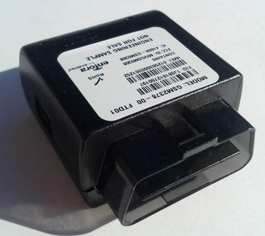
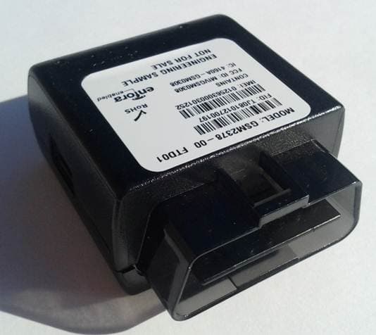
MIVGSM2378
Dec 23, 2012PCS GSM/ GPRS Licensed Transmitter
Equipment Class
PCB - PCS Licensed Transmitter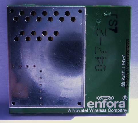
MIVCNN0301
May 10, 20121XRTT Multi-Band M2M OEM Module
Equipment Class
PCB - PCS Licensed Transmitter
MIVGSM2428
Jun 15, 2011GSM/ GPRS Personal Tracker
Equipment Class
JBP - Part 15 Class B Computing Device Peripheral
MIVGSM5218
Mar 15, 2011GSM/GPRS Asset Tracker
Equipment Class
PCB - PCS Licensed Transmitter