MSQMWOM4LAMOTHERBOARD
ASUSTeK Computer Inc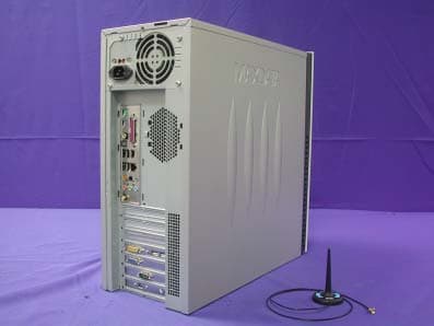
Click to zoom
Application Details
- Equipment Class
- DTS - Digital Transmission System
- Date of Grant
- Dec 20, 2004
- Application Purpose
- Original Equipment
- Date of Application
- Dec 20, 2004
- Equipment Note
- MOTHERBOARD
- Frequency Range
- 2412.00000000 - 2462.00000000
- Company
- ASUSTeK Computer Inc
- Country
- Taiwan
Documents & Files
Document Text
Text extracted from the exhibit documents filed with the FCC. Open a document above to read the original.
Users Manual
The users manual file size is too large. Requested from customer.
Users Manual
Motherboard A8V-E Deluxe iiii iiii ii Copyright © 2004 ASUSTeK COMPUTER INC. All Rights Reserved. No part of this manual, including the products and software described in it, may be reproduced, transmitted, transcribed, stored in a retrieval system, or translated into any language in any form or by any means, except documentation kept by the purchaser for backup purposes, without the express written permission of ASUSTeK COMPUTER INC. (“ASUS”). Product warranty or service will not be extended if: (1) the product is repaired, modified or altered, unless such repair, modification of alteration is authorized in writing by ASUS; or (2) the serial number of the product is defaced or missing. ASUS PROVIDES THIS MANUAL “AS IS” WITHOUT WARRANTY OF ANY KIND, EITHER EXPRESS OR IMPLIED, INCLUDING BUT NOT LIMITED TO THE IMPLIED WARRANTIES OR CONDITIONS OF MERCHANTABILITY OR FITNESS FOR A PARTICULAR PURPOSE. IN NO EVENT SHALL ASUS, ITS DIRECTORS, OFFICERS, EMPLOYEES OR AGENTS BE LIABLE FOR ANY INDIRECT, SPECIAL, INCIDENTAL, OR CONSEQUENTIAL DAMAGES (INCLUDING DAMAGES FOR LOSS OF PROFITS, LOSS OF BUSINESS, LOSS OF USE OR DATA, INTERRUPTION OF BUSINESS AND THE LIKE), EVEN IF ASUS HAS BEEN ADVISED OF THE POSSIBILITY OF SUCH DAMAGES ARISING FROM ANY DEFECT OR ERROR IN THIS MANUAL OR PRODUCT. SPECIFICATIONS AND INFORMATION CONTAINED IN THIS MANUAL ARE FURNISHED FOR INFORMATIONAL USE ONLY, AND ARE SUBJECT TO CHANGE AT ANY TIME WITHOUT NOTICE, AND SHOULD NOT BE CONSTRUED AS A COMMITMENT BY ASUS. ASUS ASSUMES NO RESPONSIBILITY OR LIABILITY FOR ANY ERRORS OR INACCURACIES THAT MAY APPEAR IN THIS MANUAL, INCLUDING THE PRODUCTS AND SOFTWARE DESCRIBED IN IT. Products and corporate names appearing in this manual may or may not be registered trademarks or copyrights of their respective companies, and are used only for identification or explanation and to the owners’ benefit, without intent to infringe. E1781E1781 E1781E1781 E1781 First EditionFirst Edition First EditionFirst Edition First Edition December 2004December 2004 December 2004December 2004 December 2004 iiiiii iiiiii iii Contents Notices............................................................................................... vii Safety information ............................................................................ viii About this guide ................................................................................. ix How this guide is organized .................................................... ix Where to find more information .............................................. ix Conventions used in this guide ................................................x Typography..........................................................................................x A8V-E Deluxe specifications summary ............................................... xi Chapter 1: Product introductionChapter 1: Product introduction Chapter 1: Product introductionChapter 1: Product introduction Chapter 1: Product introduction 1.1 Welcome!.............................................................................. 1-1 1.2 Package contents ................................................................. 1-1 1.3 Special features.................................................................... 1-2 1.3.1 Product highlights................................................... 1-2 1.3.2 ASUS Proactive features ........................................ 1-4 1.3.3 Innovative ASUS features ....................................... 1-5 Chapter 2: Hardware informationChapter 2: Hardware information Chapter 2: Hardware informationChapter 2: Hardware information Chapter 2: Hardware information 2.1 Before you proceed .............................................................. 2-1 2.2 Motherboard overview.......................................................... 2-2 2.2.1 Placement direction ................................................ 2-2 2.2.2 Screw holes ............................................................ 2-2 2.2.3 Motherboard layout ................................................ 2-3 2.2.4 Layout Contents..................................................... 2-4 2.3 Central Processing Unit (CPU) .............................................. 2-6 2.3.1 Overview................................................................. 2-6 2.3.2 Installling the CPU................................................... 2-6 2.3.3 Installing the heatsink and fan................................ 2-8 2.4 System memory .................................................................2-10 2.4.1 Overview...............................................................2-10 2.4.2 Memory Configurations.........................................2-11 2.4.3 Installing a DIMM ...................................................2-13 2.4.4 Removing a DIMM .................................................2-13 2.5 Expansion slots...................................................................2-14 2.5.1 Installing an expansion card..................................2-14 2.5.2 Configuring an expansion card..............................2-14 iviv iviv iv Contents 2.5.3 Interrupt assignments ..........................................2-17 2.5.4 PCI slots................................................................2-18 2.5.5 PCI Express x16 slot .............................................2-18 2.5.6 PCI Express x1 slot ...............................................2-18 2.6 Jumpers ..............................................................................2-19 2.7 Connectors .........................................................................2-22 2.7.1 Rear panel connectors ..........................................2-22 2.7.2 Internal connectors...............................................2-24 Chapter 3: Powering upChapter 3: Powering up Chapter 3: Powering upChapter 3: Powering up Chapter 3: Powering up 3.1 Starting up for the first time................................................ 3-1 3.…
Text truncated - open the document above for the full version.
Users Manual
4 BIOS setup This chapter tells how to change the system settings through the BIOS Setup menus. Detailed descriptions of the BIOS parameters are also provided. ASUS A8V-E DeluxeASUS A8V-E Deluxe ASUS A8V-E DeluxeASUS A8V-E Deluxe ASUS A8V-E Deluxe Chapter summary 4.1 Managing and updating your BIOS........................................ 4-1 4.2 BIOS setup program ...........................................................4-11 4.3 Main menu ..........................................................................4-15 4.4 Advanced menu..................................................................4-18 4.5 Power menu........................................................................4-33 4.6 Boot menu..........................................................................4-37 4.7 Exit menu ...........................................................................4-44 ASUS A8V-E DeluxeASUS A8V-E Deluxe ASUS A8V-E DeluxeASUS A8V-E Deluxe ASUS A8V-E Deluxe 4-14-1 4-14-1 4-1 4.1 Managing and updating your BIOS The following utilities allow you to manage and update the motherboard Basic Input/Output System (BIOS) setup. 1. AwardBIOS Flash Utility AwardBIOS Flash Utility AwardBIOS Flash Utility AwardBIOS Flash Utility AwardBIOS Flash Utility (Updates the BIOS in DOS mode using a bootable floppy disk.) 2. ASUS CrashFree BIOS 2 ASUS CrashFree BIOS 2 ASUS CrashFree BIOS 2 ASUS CrashFree BIOS 2 ASUS CrashFree BIOS 2 (Updates the BIOS using a bootable floppy disk or the motherboard support CD when the BIOS file fails or gets corrupted.) 3. ASUS EZ Flash ASUS EZ Flash ASUS EZ Flash ASUS EZ Flash ASUS EZ Flash (Updates the BIOS in DOS using a floppy disk or the motherboard support CD.) 4. ASUS Update ASUS Update ASUS Update ASUS Update ASUS Update (Updates the BIOS in Windows ® environment.) Refer to the corresponding sections for details on these utilities. 4.1.14.1.1 4.1.14.1.1 4.1.1 Creating a bootable floppy diskCreating a bootable floppy disk Creating a bootable floppy diskCreating a bootable floppy disk Creating a bootable floppy disk 1. Do either one of the following to create a bootable floppy disk. DOS environment a. Insert a 1.44MB floppy disk into the drive. b. At the DOS prompt, type format A:/S then press <Enter>. Windows ® XP environment a. Insert a 1.44 MB floppy disk to the floppy disk drive. b. Click Start Start Start Start Start from the Windows ® desktop, then select MyMy MyMy My ComputerComputer ComputerComputer Computer. c. Select the 3 1/2 Floppy Drive icon. d. Click File File File File File from the menu, then select FormatFormat FormatFormat Format. A Format 3 1/2Format 3 1/2 Format 3 1/2Format 3 1/2 Format 3 1/2 Floppy DiskFloppy Disk Floppy DiskFloppy Disk Floppy Disk window appears. e. Select Create an MS-DOS startup disk Create an MS-DOS startup disk Create an MS-DOS startup disk Create an MS-DOS startup disk Create an MS-DOS startup disk from the format options field, then click StartStart StartStart Start. Windows ® 2000 environment To create a set of boot disks for Windows ® 2000: a. Insert a formatted, high density 1.44 MB floppy disk into the drive. b. Insert the Windows ® 2000 CD to the optical drive. Save a copy of the original motherboard BIOS file to a bootable floppy disk in case you need to restore the BIOS in the future. Copy the original motherboard BIOS using the ASUS Update or AwardBIOS Flash utilities. 4-24-2 4-24-2 4-2 Chapter 4: BIOS setupChapter 4: BIOS setup Chapter 4: BIOS setupChapter 4: BIOS setup Chapter 4: BIOS setup c. Click StartStart StartStart Start, then select RunRun RunRun Run. d. From the Open field, type D:\bootdisk\makeboot a: assuming that D: is your optical drive. e. Press <Enter>, then follow screen instructions to continue. 2. Copy the original or the latest motherboard BIOS file to the bootable floppy disk. 4.1.24.1.2 4.1.24.1.2 4.1.2 Updating the BIOSUpdating the BIOS Updating the BIOSUpdating the BIOS Updating the BIOS The Basic Input/Output System (BIOS) can be updated using the AwardBIOS Flash Utility. Follow these instructions to update the BIOS using this utility. 1. Download the latest BIOS file from the ASUS web site. Rename the file to A8V-E.BINA8V-E.BIN A8V-E.BINA8V-E.BIN A8V-E.BIN and save it to a floppy disk. Save only the updated BIOS file in the floppy disk to avoid loading the wrong BIOS file. 2. Copy the AwardBIOS Flash Utility (awdflash.exe) from the Software folder of the support CD to the floppy disk with the latest BIOS file. 3. Boot the system in DOS mode using the bootable floppy disk you created earlier. 4. When the A:>A:> A:>A:> A:> appears, replace the bootable floppy disk with the floppy disk containing the new BIOS file and the Award BIOS Flash Utility. 5. At the prompt, type awdflashawdflash awdflashawdflash awdflash then press <Enter>. The Award BIOS Flash Utility screen appears. AwardBIOS Flash Utility for ASUS V1.01 (C) Phoenix Technologies Ltd. All Rights Reserved Message: Please input File Name! For K8T890-8237-A8V-E-00 DATE: 09/10/2004 Flash Type - PMC Pm49FL004T LPC/FWH File Name to Program: ASUS A8V-E DeluxeASUS A8V-E Deluxe ASUS A8V-E DeluxeASUS A8V-E Deluxe ASUS A8V-E Deluxe 4-34-3 4-34-3 4-3 6. Type the BIOS file name in the File Name toFile Name to File Name toFile Name to File Name to ProgramProgram ProgramProgram Program field, then press <Enter>. Do not turn off or reset the system during the flashing process! AwardBIOS Flash Utility for ASUS V1.01 (C) Phoenix Technologies Ltd. All Rights Reserved For K8T890-8237-A8V-E-00 DATE: 09/10/2004 Flash Type - PMC Pm49FL004T LPC/FWH File Name to Program: A8V-E.BIN AwardBIOS Flash Utility for ASUS V1.01 (C) Phoenix Technologies Ltd. All Rights Reserved Warning: Don’t Turn Off Power Or Reset System! For K8T890-8237-A8V-E-00 DATE: 09/10/2004 Flash Type - PMC Pm49FL004T LPC/FWH File Name to Program: A8V-E.BIN Program Flashing Memory - OFE00 OK Write OK No Update Write Fail 123 1 23 1 23 123 1234567890123456789012345678901 1 234567890123456789012…
Text truncated - open the document above for the full version.
Block Diagram
5 5 4 4 3 3 2 2 1 1 DD CC BB AA HYPERTRANSPORT 939PSOCKET AMD K8 A8V-E Deluxe 16 bit X 16 bit VT 8237 South Bridge PCI Slot x 3 North Bridge K8T890PRO 1GHz SATA1 SATA2 Serial ATA IDE BUS Primary IDE Secondary IDE USB 8 x USB2.0 VT 6307 1394 Controller VIA PDC 20378 PROMISE Super IO Winbond V-Link BUS1GHz FWH Parallel Port FDD COM1,COM2 BIOS VT6420 PS/2 KB Mouse PS2/MOUSE 850 AC97 Codec AC-LINK ALC W83627EHF Channel B DDR SDRAM DIMM x 2 DDR SDRAM DIMM x 2 Revision : 1.00 PC 3200MEM BUS Channel A LPC BUS PCI BUS AGP Slot Ethernet Controller MARVELL PCI-E X1 PCI-E X1 PCI-E X1 AGP BUS PCI-E BUS PCI-EX16 Slot 16 Lane Link 939-1 23 939-2 Q-FAN USB2.0 45 15 939-5 DDR Termination2 06 TITLE ASIC8282 Marvell 88E8053 K8T890-1 40 DDR A1/A2 31 3VSB/2.5VSB/DUAL_VTT_DDR Audio-Mute LPT,COM VT8237-2 DDR Termination1 22 WIFI-1 IEEE 1394 19 35 K8T890-2 24 38 29 Audio-ALC850 PCIEX16 16 41 11 BAT&ATX 939-3 27 WIFI-2 SIO PCIEX1 03 939-4 07 PAGE 39 04 WIFI-3 Sili 3114 VT8237-4 37 32 46 09 42 05 10 VT8237-3 Block Diagram 20 43 25 33 Audio-Panel K8T890-3 44 28 26 13 14 DOC&2.5V,1.5V,1.2V,VTT_DDR VT8237-1 12 Main Clock 34+1.8V&3V,5V-DUAL 01 36 K8_SEMTECH_3PHASE-VCORE AGP 21 17 History ASIC007&Game Port PCI 02 DDR B1/B2 30 18 08 Power Flow BIOS/PANEL/SPEECH IDE EMI CPUFAN 49 48 47 Power Sequence WIFI A3 147Tuesday, August 17, 2004 ASUSTEK COMPUTER INC BLOCK 1.00 A8V-E Oldy_Chu <Core Design> SizeProject Name Rev Date:Sheetof Title : Engineer:
External Photos
Report No.: 04AL016FI Page : 1 of 3 Version:1.0 Attachment 2 : EUT Detailed Photographs (1) EUT Photo (2) EUT Photo
ID Label/Location Info
ASUSTek COMPUTER INC. FCC ID.: MSQMWOM4LA 4FL., No. 150, Li-Te Rd., Peitou, Taipei, Taiwan, R.O.C. Tel: +886 2 2894-3447 FCC ID AND DoC Label The FCC ID and DoC Label will be placed on the equipment as shown in the photograph below. Motherboard ATIO Model No.: A8V-E Deluxe Motherboard Model No.: A8V-E Deluxe F F C C C C I I D D : : M M S S Q Q M M W W O O M M 4 4 L L A A This device complies with Part 15 of the FCC Rules. Operation is subject to the following two conditions: (1) this device may not cause harmful interference and (2) this device must accept any interference received, including interference that may cause undesired operation. S/N: Made in Taiwan
ID Label/Location Info
ASUSTek COMPUTER INC. FCC ID.: MSQMWOM4LA 4FL., No. 150, Li-Te Rd., Peitou, Taipei, Taiwan, R.O.C. Tel: +886 2 2894-3447 FCC ID AND DoC Label The FCC ID and DoC Label will be placed on the equipment as shown in the photograph below. Motherboard ATIO Model No.: A8V-E Deluxe Motherboard Model No.: A8V-E Deluxe F F C C C C I I D D : : M M S S Q Q M M W W O O M M 4 4 L L A A This device complies with Part 15 of the FCC Rules. Operation is subject to the following two conditions: (1) this device may not cause harmful interference and (2) this device must accept any interference received, including interference that may cause undesired operation. S/N: Made in Taiwan
Internal Photos
Report No.: 04AL016FI Page : 2 of 3 Version:1.0 (3) EUT Photo (4) EUT Photo Report No.: 04AL016FI Page : 3 of 3 Version:1.0 (5) EUT Photo (6) EUT Photo
Operational Description
Report No. 04AL016FI Page: 5 of 64 Version:1.0 1.2. Operational Description EUT is a Motherboard with 11 channels. This device provided four kinds of transmitting speed 1, 2, 5.5 and 11Mbps. The device of RF carrier is DQPSK, DB PSK and CCK (IEEE 802.11b) or eight kinds of transmitting speed 6, 9, 12, 18, 24, 36, 48 and 54Mbps. The device of RF carrier is OFDM (IEEE 802.11g). The device adapts direct sequence spread spectrum modulation. The antenna was Connector provides diversity function to improve the receiving function. This Motherboard, compliant with IEEE 802.11b and IEEE 802.11g, is a high-efficiency Wireless LAN adapter. It allows your computer to connect to a wireless network and to share resources, such as files or printers without being bound to the network wires. Operation in 2.4GHz Direst Sequence Spread Spectrum (DSSS) radio transmission, the Motherboard Wired Equivalent Protection (WEP) algorithm is used. In addition, its standard compliance ensures that it can communicate with any IEEE 802.11b and IEEE 802.11g network. Test Mode: Mode 1: Transmitter 802.11b (INPAQ) Mode 1: Transmitter 802.11g (INPAQ)
RF Exposure Info
Report No. 04AL016FI Page: 1 of 3 Version: 1.0 RF Exposure Evaluation declaration Product Name : Motherboard Model No. : A8V-E Deluxe FCC ID MSQMWOM4LA Applicant : ASUSTeK COMPUTER INC. Address : 4FL., No. 150, Li-Te Rd., Peitou, Taipei, Taiwan, R.O.C. Date of Receipt : Sep. 30, 2004 Date of Declaration: Oct. 14, 2004 Report No. : 04AL016FI The declaration results relate only to the samples calculated. The declaration shall not be reproduced except in full without the written approval of QuieTek Corporation. This report must not be used to claim product endorsement by NVLAP any agency of the U.S. Government Report No. 04AL016FI Page: 2 of 3 Version: 1.0 1. RF Exposure Evaluation 1.1. Limits According to FCC 1.1310: The criteria listed in the following table shall be used to evaluate the environment impact of human exposure to radio frequency (RF) radiation as specified in 1.1307(b) LIMITS FOR MAXIMUM PERMISSIBLE EXPOSURE (MPE) Frequency Range (MHz) Electric Field Strength (V/m) Magnetic Field Strength (A/m) Power Density (mW/cm 2 ) Average Time (Minutes) (A) Limits for Occupational/ Control Exposures 300-1500 -- -- F/300 6 1500-100,000 -- -- 5 6 (B) Limits for General Population/ Uncontrolled Exposures 300-1500 -- -- F/1500 6 1500-100,000 -- -- 1 30 F= Frequency in MHz Friis Formula Friis transmission formula: Pd = (Pout*G)/(4*pi*r 2 ) Where Pd = power density in mW/cm 2 Pout = output power to antenna in mW G = gain of antenna in linear scale Pi = 3.1416 R = distance between observation point and center of the radiator in cm Pd id the limit of MPE, 1 mW/cm 2 . If we know the maximum gain of the antenna and the total power input to the antenna, through the calculation, we will know the distance r where the MPE limit is reached. 1.2. Test Procedure Software provided by client enabled the EUT to transmit and receive data at lowest, middle and highest channel individually. The temperature and related humidity: 18and 78 RH. Report No. 04AL016FI Page: 3 of 3 Version: 1.0 1.3. Test Result of RF Exposure Evaluation Product : Motherboard Test Item : RF Exposure Evaluation Test Site : No.3 OATS Antenna Gain Antenna Gain: The maximum Gain measured in fully anechoic chamber is 2.45dBi in linear scale. 802.11b Output Power Into Antenna & RF Exposure Evaluation Distance (INPAQ: 2.45dBi): Channel Frequency (MHz) Output Power to Antenna (mW) Power Density at R = 20 cm (mW/cm2) 1 2412.00 55.5904 0.0194 6 2437.00 57.0164 0.0199 11 2462.00 64.5654 0.0226 802.11g Output Power Into Antenna & RF Exposure Evaluation Distance (INPAQ: 2.45dBi): Channel Frequency (MHz) Output Power to Antenna (mW) Power Density at R = 20 cm (mW/cm2) 1 2412.00 27.4157 0.0096 6 2437.00 26.9774 0.0094 11 2462.00 31.8420 0.0111 The distance r (4 th column) calculated from the Fries transmission formula is far shorter than 20 cm separation requirement.
Test Report
Report No. 04AL016FI Page: 1 of 64 Version:1.0 Test Report Product Name : Motherboard Model No. : A8V-E Deluxe FCC ID : MSQMWOM4LA Applicant : ASUSTeK COMPUTER INC. Address : 4FL., No. 150, Li-Te Rd., Peitou, Taipei, Taiwan, R.O.C. Date of Receipt : Sep. 30, 2004 Issued Date : Oct. 14, 2004 Report No. : 04AL016FI The test results relate only to the samples tested. The test report shall not be reproduced except in full without the written approval of QuieTek Corporation. This report must not be used to claim product endorsement by NVLAP any agency of the U.S. Government Report No. 04AL016FI Page: 2 of 64 Version:1.0 Test Report Certification Issued Date: Oct. 14, 2004 Report No. : 04AL016FI Test results relate only to the samples tested. The test report shall not be reproduced except in full without the written approval of QuieTek Corporation. This report must not be used to claim product endorsement by NVLAP any agency of the U.S. Government Product Name : Motherboard Applicant : ASUSTeK COMPUTER INC. Address : 4FL., No. 150, Li-Te Rd., Peitou, Taipei, Taiwan, R.O.C. Manufacturer : ASUSTeK COMPUTER INC. Model No. : A8V-E Deluxe Rated Voltage : AC 120V/60Hz Working Voltage : DC 3.3V Trade Name : ASUS Measurement Standard : FCC CFR Title 47 Part 15 Subpart C: 2003 Measurement Procedure : ANSI C63.4: 2001 Test Result : Complied Documented By : ( Anita Chou ) Tested By : ( Tim Sung ) Approved By : ( Gene Chang ) Accredited by NIST (NVLAP) NVLAP Lab Code: 200533-0 Report No. 04AL016FI Page: 3 of 64 Version:1.0 TABLE OF CONTENTS Description Page 1. GENERAL INFORMATION .....................................................................................................4 1.1. EUT Description............................................................................................................................4 1.2. Operational Description ................................................................................................................5 1.3. Tested System Datails....................................................................................................................6 1.4. Configuration of Tested System ....................................................................................................7 1.5. EUT Exercise Software .................................................................................................................7 1.6. Test Facility ...................................................................................................................................8 2. Conducted Emission....................................................................................................................9 2.1. Test Equipment..............................................................................................................................9 2.2. Test Setup ......................................................................................................................................9 2.3. Limits ............................................................................................................................................9 2.4. Test Procedure .............................................................................................................................10 2.5. Uncertainty ..................................................................................................................................10 2.6. Test Result of Conducted Emission.............................................................................................11 3. Peak Power Output ...................................................................................................................15 3.1. Test Equipment............................................................................................................................15 3.2. Test Setup ....................................................................................................................................15 3.3. Limits ..........................................................................................................................................15 3.4. Uncertainty ..................................................................................................................................15 3.5. Test Result of Peak Power Output...............................................................................................16 4. Radiated Emission .....................................................................................................................18 4.1. Test Equipment............................................................................................................................18 4.2. Test Setup ....................................................................................................................................18 4.3. Limits ..........................................................................................................................................19 4.4. Test Procedure .............................................................................................................................20 4.5. Uncertainty ..................................................................................................................................20 4.6. Test Result of Radiated Emission................................................................................................21 5. Band Edge ..................................................................................................................................33 5.1. Test Equipment............................................................................................................................33 5.2. Test Setup ....................................................................................................................................33 5.3. Limits .................................................................…
Text truncated - open the document above for the full version.
Test Setup Photos
Report No.: 04AL016FI Page : 1 of 3 Version:1.0 Attachment 1: EUT Test Setup Photographs Front View of Conducted Test Back View of Conducted Test Report No.: 04AL016FI Page : 2 of 3 Version:1.0 Front View of Radiated Test Back View of Radiated Test Report No.: 04AL016FI Page : 3 of 3 Version:1.0 Front View of Radiated Test (Horn) Back View of Radiated Test (Horn)
Contact Information
Applicant
Jackson Yen(Associate Vice President)
Test Firm
DEKRA Testing and Certification Co., Ltd.Sky Hsu
Technical Specifications
| # | Rule Parts | Frequency Range | Power Output |
|---|---|---|---|
| 1 | 15C | 2.41 GHz - 2.46 GHz | 64.56 mW |
Other Applications from ASUSTeK Computer Inc
MSQ-GC701
Aug 21, 2026Wireless Gaming Controller
Equipment Class
DSS - Part 15 Spread Spectrum TransmitterMSQMPDONGLE3
Aug 18, 2026WIRELESS DONGLE
Equipment Class
DTS - Digital Transmission System
MSQ-GC701D
Aug 13, 2026USB Wireless Dongle
Equipment Class
DSS - Part 15 Spread Spectrum TransmitterMSQ-CM3206DM4A
May 27, 2026Chromebook/Notebook PC
Equipment Class
DCD - Part 15 Low Power Transmitter Below 1705 kHz
MSQ-GST868003
Apr 03, 2026MODULE-WIRELESS CHRG
Equipment Class
DCD - Part 15 Low Power Transmitter Below 1705 kHz