MSQPCCWL120WLAN mini-PCI card
ASUSTeK Computer Inc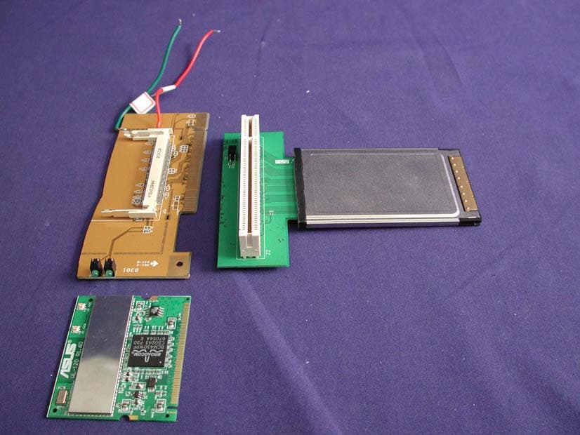
Click to zoom
Application Details
- Equipment Class
- DTS - Digital Transmission System
- Date of Grant
- Apr 21, 2003
- Application Purpose
- Original Equipment
- Date of Application
- Apr 14, 2003
- Equipment Note
- WLAN mini-PCI card
- Frequency Range
- 2412.00000000 - 2462.00000000
- Company
- ASUSTeK Computer Inc
- Country
- Taiwan
Documents & Files



Document Text
Text extracted from the exhibit documents filed with the FCC. Open a document above to read the original.
Users Manual
ASUS WLAN mini-PCI card WL-120 User Manual 2ASUS WLAN mini-PCI card No part of this manual, including the products and software described in it, may be reproduced, transmitted, transcribed, stored in a retrieval system, or translated into any language in any form or by any means, except docu- mentation kept by the purchaser for backup purposes, without the express written permission of ASUSTeK COMPUTER INC. (“ASUS”). ASUS PROVIDES THIS MANUAL “AS IS” WITHOUT WARRANTY OF ANY KIND, EITHER EXPRESS OR IMPLIED, INCLUDING BUT NOT LIMITED TO THE IMPLIED WARRANTIES OR CONDITIONS OF MERCHANTABILITY OR FITNESS FOR A PARTICULAR PUR- POSE. IN NO EVENT SHALL ASUS, ITS DIRECTORS, OFFICERS, EMPLOYEES OR AGENTS BE LIABLE FOR ANY INDIRECT, SPE- CIAL, INCIDENTAL, OR CONSEQUENTIAL DAMAGES (INCLUD- ING DAMAGES FOR LOSS OF PROFITS, LOSS OF BUSINESS, LOSS OF USE OR DATA, INTERRUPTION OF BUSINESS AND THE LIKE), EVEN IF ASUS HAS BEEN ADVISED OF THE POSSIBILITY OF SUCH DAMAGES ARISING FROM ANY DEFECT OR ERROR IN THIS MANUAL OR PRODUCT. Product warranty or service will not be extended if: (1) the product is re- paired, modified or altered, unless such repair, modification of alteration is authorized in writing by ASUS; or (2) the serial number of the product is defaced or missing. Products and corporate names appearing in this manual may or may not be registered trademarks or copyrights of their respective companies, and are used only for identification or explanation and to the owners’ benefit, without intent to infringe. SPECIFICATIONS AND INFORMATION CONTAINED IN THIS MANUAL ARE FURNISHED FOR INFORMATIONAL USE ONLY, AND ARE SUBJECT TO CHANGE AT ANY TIME WITHOUT NOTICE, AND SHOULD NOT BE CONSTRUED AS A COMMITMENT BY ASUS. ASUS ASSUMES NO RESPONSIBILITY OR LIABILITY FOR ANY ERRORS OR INACCURACIES THAT MAY APPEAR IN THIS MANUAL, IN- CLUDING THE PRODUCTS AND SOFTWARE DESCRIBED IN IT. Copyright © 2003 ASUSTeK COMPUTER INC. All Rights Reserved. Copyright Information Product Name: ASUS WLAN mini-PCI card (WL-120) Manual Revision:1 E1219 Release Date:March 2003 ASUS WLAN mini-PCI card 3 Copyright Information ASUSTeK COMPUTER INC. (Asia-Pacific) Address:150 Li-Te Road, Peitou, Taipei, Taiwan 112 General Tel:+886-2-2894-3447 General Fax:+886-2-2894-3449 General Email: [email protected] Technical Support MB/Others (Tel): +886-2-2890-7121 (English) Notebook (Tel): +886-2-2890-7122 (English) Desktop/Server: +886-2-2890-7123 (English) Support Fax:+886-2-2890-7698 Support Email: [email protected] Web Site:www.asus.com.tw ASUS COMPUTER INTERNATIONAL (America) Address:44370 Nobel Drive, Fremont, CA 94538, USA General Fax:+1-510-608-4555 General Email: [email protected] Technical Support Support Fax:+1-510-608-4555 General Support: +1-502-933-8713 Web Site:www.asus.com Support Email: [email protected] ASUS COMPUTER GmbH (Germany & Austria) Address:Harkortstr. 25, 40880 Ratingen, BRD, Germany General Fax:+49-2102-442066 General Email: [email protected] (for marketing requests only) Technical Support Support Hotline: MB/Others: +49-2102-9599-0 Notebook (Tel): +49-2102-9599-10 Support Fax:+49-2102-9599-11 Support (Email): www.asuscom.de/de/support (for online support) Web Site:www.asuscom.de ASUS WLAN mini-PCI card 4 Quick Start Guide Chapter 1 Welcome The ASUS WLAN mini-PCI card is designed to be fully compliant with the IEEE 802.11b wireless local area network (Wireless LAN) standard. The ASUS WLAN mini-PCI card comes with two antenna connectors, which are individually connected to the built-in antennas in your notebook. The two antennas allow your notebook to have the best communication when you are enjoying the wireless link. Verifying the TCP/IP Protocol Windows 98/Me Right-click My Network Placeon the desktop and select properties. Scroll down and look for "TCP/IP -> ASUS 802.11b Network Adap- ter". Make sure that the TCP/IP protocal parameters (IP adress, gate- way, and subnet mask) are set correctly. Windows 2K/XP Open the Control Panel through the Start menu. Double-click Network Connection icon. Right click " ASUS 802.11b Network Adapter" and sel- ect Properties. Look for "Internet Protocal (TCP/IP)". Make sure that the TCP/IP protocal parameters (IP adress, gateway, and subnet mask) are set correctly. ASUS WLAN mini-PCI card 5 Quick Start Guide Chapter 5 Installing the WLAN mini-PCI card Utilities After you have installed the WLAN mini-PCI card driver, you can install WLAN mini-PCI card utilities. Refer to the User's manual for detailed information. 1. Insert the ASUS WLAN mini-PCI card support CD and an autorun menu will appear. If your autorun is disabled, double click SETUP.EXE in the root directory of the support CD. 2. From the autorun menu, click Install ASUS WLAN mini-PCI card Utilities. 3. Follow the on-screen instructions to complete the installation. Statement This device is intended only for OEM integrators under the following conditions: 1. The antenna must be installed such that 20 cm is maintained between the antenna and users. 2. The transmitter module may not be co-located with any other transmitter or antenna. 3. For laptop installations, the antenna must be installed to ensure that the proper spacing is maintained in the event the device is used in held-on- lap positions (i.e. positioning of antennas must be placed in the upper portion of the LCD panel only to ensure 20 cm will be maintained if the user places the device on their lap for use). The card must cease to transmit with the lid shut to prevent transmission in portable operating conditions. As long as the conditions above are met, further transmitter test will not be required. However, the OEM integrator is still responsible for testing their end-product for any additional compliance requirements required with this module installed (for example, digital device emissions, PC peripheral requirements, etc.). IMPORTANT NOTE: In the event that these conditions can not be met (for example certain laptop configurations or co-location with another transmitter), th…
Text truncated - open the document above for the full version.
Block Diagram
WL-120 Block Diagram & Operation Discription 1. Block Diagram :
External Photos
Report No.: 034L004FI Page: 1 of 6 Version:1.0 Attachment 2 : EUT Detailed Photographs (1) EUT Photo (2) EUT Photo
ID Label/Location Info
ASUSTeK COMPUTER INC. 4FL., No, 150, Li-Te Rd., Peitou, Taipei, Taiwan, R.O.C. TEL: 886-2-28943447 FAX: 886-2-28907965 FCC ID: MSQPCCWL120 FCC ID and DoC Label WLAN mini-PCI card Model No.: WL-120 TESTED TO COMPLY WITH FCC STANDARDS FOR HOME OR OFFICE USE S/N: Made in Taiwan The FCC ID and DoC Label will be placed on the equipment as shown in the photograph below.
ID Label/Location Info
ASUSTeK COMPUTER INC. 4FL., No, 150, Li-Te Rd., Peitou, Taipei, Taiwan, R.O.C. TEL: 886-2-28943447 FAX: 886-2-28907965 FCC ID: MSQPCCWL120 FCC ID and DoC Label WLAN mini-PCI card Model No.: WL-120 TESTED TO COMPLY WITH FCC STANDARDS FOR HOME OR OFFICE USE S/N: Made in Taiwan The FCC ID and DoC Label will be placed on the equipment as shown in the photograph below.
Internal Photos
Report No.: 034L004FI Page: 2 of 6 Version:1.0 (3) EUT Photo (4) EUT Photo Report No.: 034L004FI Page: 3 of 6 Version:1.0 (5) EUT Photo (6) EUT Photo Report No.: 034L004FI Page: 4 of 6 Version:1.0 (7) EUT Photo (8) EUT Photo Report No.: 034L004FI Page: 5 of 6 Version:1.0 (9) EUT Photo (10) EUT Photo Report No.: 034L004FI Page: 6 of 6 Version:1.0 (11) EUT Photo (12) EUT Photo
Operational Description
Report No. 034L004FI Page: 6 of 45 Version:1.0 1.2. Operational Description EUT is a WLAN mini-PCI card with wireless LAN adapter. This device provided 11 channels and four kind of transmitting speed 1,2,5.5 and 11Mbps. The device of RF carrier is DQPSK, DB PSK and CCK. The device adapts direct sequence spread spectrum modulation. The Connector antenna was provides diversity function to improve the receiving function. This WLAN mini-PCI card is an IEEE 802.11b Wireless LAN adapter. It allows your computer to connect to a wireless network and to share resources, such as files or printers without being bound to the network wires. Operation in 2.4GHz Direst Sequence Spread Spectrum (DSSS) radio transmission, the WLAN mini-PCI card transfers data at speeds up to 64/128-bit Wired Equivalent Protection (WEP) algorithm is used. In addition, its standard compliance ensures that it can communicate with any 802.11b network.
Operational Description
ASUS SpaceLink Wireless LAN Mini-PCI Card WL-120 IEEE 802.11b 11 Mbps [features] z Embedded to any notebook with mPCI type IIIA slot z Seamless roaming between home, office and café shop with profiles auto-switch z Online trouble shooting tool eliminate any confusions during enjoy your wireless networking z Site survey tool to ease the wireless networking topology optimization z Secure 40/128-bit WEP with periodically change keys z Comply to Windows XP WLAN support functions [Specifications] Host interface 32-bit Mini-PCI interface, type IIIA, 3.3V only Network Standard IEEE 802.11b Data Rate 11 Mbps with automatic fallback to 5.5, 2 and 1 Mbps ; CH14 : 2 & 1 Mbps . Modulation CCK (11Mbps, 5.5Mbps), DQPSK (2Mbps), DBPSK (1Mbps) Technology Direct Sequence Spread Spectrum Network Architecture Types Infrastructure and ad-hoc Operating Frequency 2.412-2.462 GHz (N. America); 2.412-2.484 GHz (Japan); 2.412-2.472 GHz (Europe ETSI); 2.457-2.462 GHz (Spain); 2.457-2.472 GHz (France) Operating Channels CH1~CH13 for Worldwide, CH1~CH14 Japan,Thailand, CH5~CH7 Israel , CH10~CH13 Jordan , RF Output Power 14 ~ 17 dBm ; Channel 14 : 12.5~15dBm. (at nominal temp. range) Antenna connectors There are two antenna connector, mark as MAIN and AUX. Transmission through MAIN antenna, and support receiving diversity through both antenna. The antenna ports is 50 ohms nominal impedance, with a VSWR of 1.5:1 maximum in the frequency band of interest Range Indoor 100 ft (30 m), semi-open 200 ft (60 m), outdoor (LOS, Light-Of-Sight) 600 ft (180 m) at 11Mbps The range may vary by different environment Receiver Sensitivity PER< 8% @ length=1024 octets (at nominal temp. range) 11Mbps: -82 ~ -85 dBm; 5.5Mbps: -85 ~ -88 dBm; 2 Mbps: -88 ~ -91 dBm; 1 Mbps: -91 ~ -93 dBm Power Consumption TX power consumption:350~450 mA RX power consumption :250~350 mA WEP 40/128-bit WEP; each includes 4 user-defined keys; periodically change key to maximize security Utilities Mobile control center: Integrate all tools and indicate real time status information on system tray Wireless setting: Diagnose and configure your wireless network settings with on-line trouble shooting feature. Mobile manager: Support automatic roaming and network reconfiguration between different locations Site survey: Explore your wireless networking topology through a handy way Live Update: Download the newest driver and utilities from Internet Windows XP Compatibility Native support for all built-in WLAN functions, like Zeroconfig, Media Sense and 802.1x Support OS Windows 98, ME, 2000, NT 4, XP, CE 3.0, Pocket PC 2002 and Linux LED Indicators 1. WLAN Activity Indicator The LED_WLAN_Activity output signal from Pin11 of the MPCI system connector is named LED_WLAN_ACTIVITY. This pin will provide a 7mA source current for 3.3V LED operation. The operation of the LED is: ON (3.3V) = There is WLAN activity ongoing (packets are being sent or received), AND the card is already associated. If the card is not associated, this LED will remain OFF. It is required that this LED will flash in accordance with the activity such that higher levels of activity result in the LED being ON longer. OFF (low) = The WLAN card is not associated. If it is associated, then the LED remains OFF while there is no WLAN activity ongoing. 2. WLAN Radio State Indicator The LED_WLAN_RadioState output signal from Pin12 of the MPCI system connector is named LED_WLAN_RADIO_ON. This signal will reflect the actual state of the radio, and not the state of a user setting, software, switch or anything else. This pin will provide a 7mA source current for 3.3V LED operation. ON (3.3V) = The WLAN radio is on, and is capable of transmitting. The LED is ON even if the radio is not actually transmitting. If the card has a way of independently turning off the transmit section, then this LED is ON when the transmitter section is in any state that is capable of transmitting. OFF (low) = The WLAN radio is NOT capable of transmitting unless the user performs some action to change the state of the radio. Operating Temperature -10 ~ 55°C Storage Temperature -40~ 70°C Humidity (non-condensing) 5~95% Emissions ETS 300 328 and ETS 300 826; CE Mark; FCC Part 15C, Section 15.247 Size 60 mm L* 50.1 mm W* 2.5 mm H(± 0.2) Weight 10 g [Pictures] MPCI Card MPCI Antenna Connector Placement MA 59.75 41.7 53.7 50. 95 48. 3
Parts List/Tune Up Info
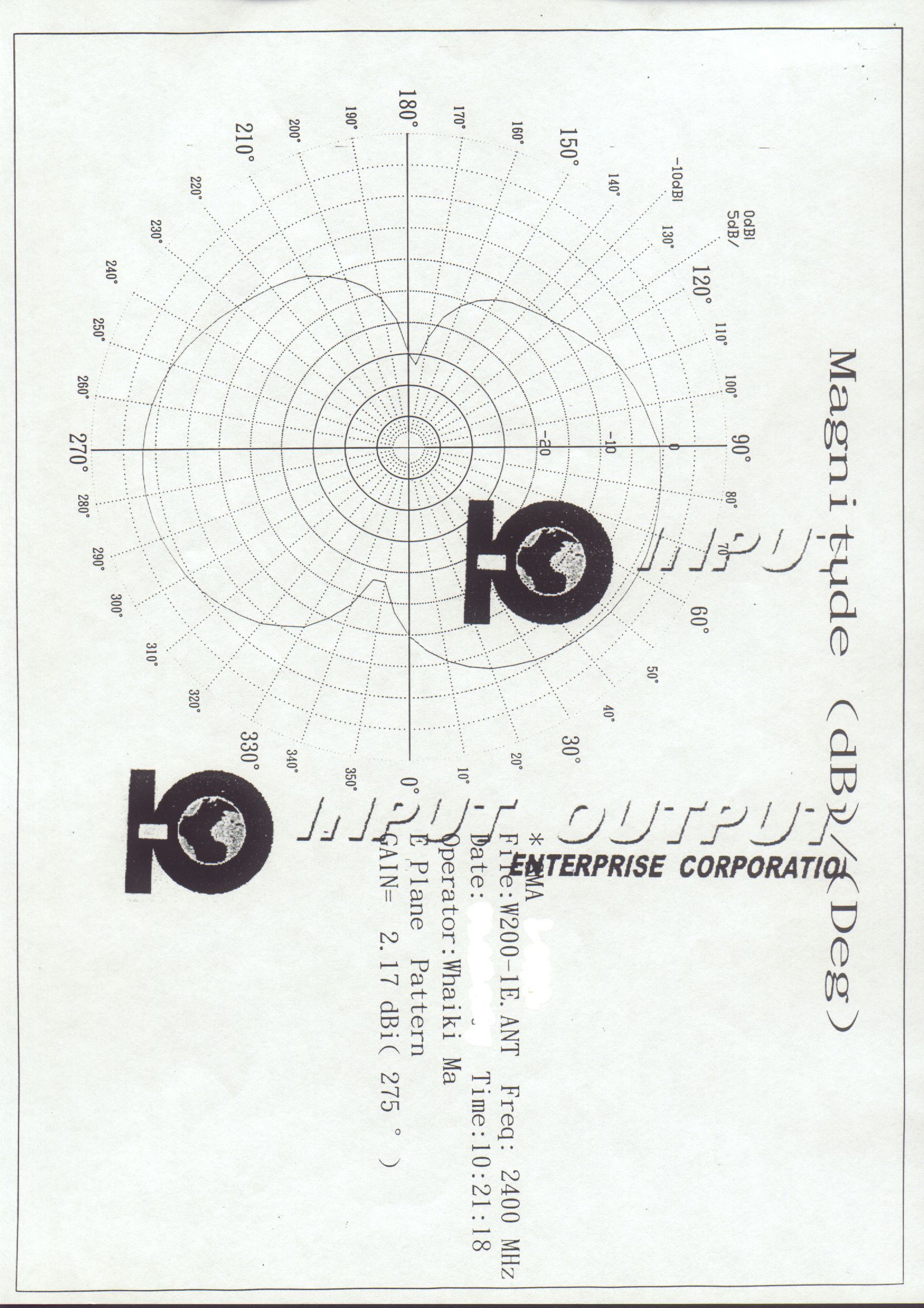
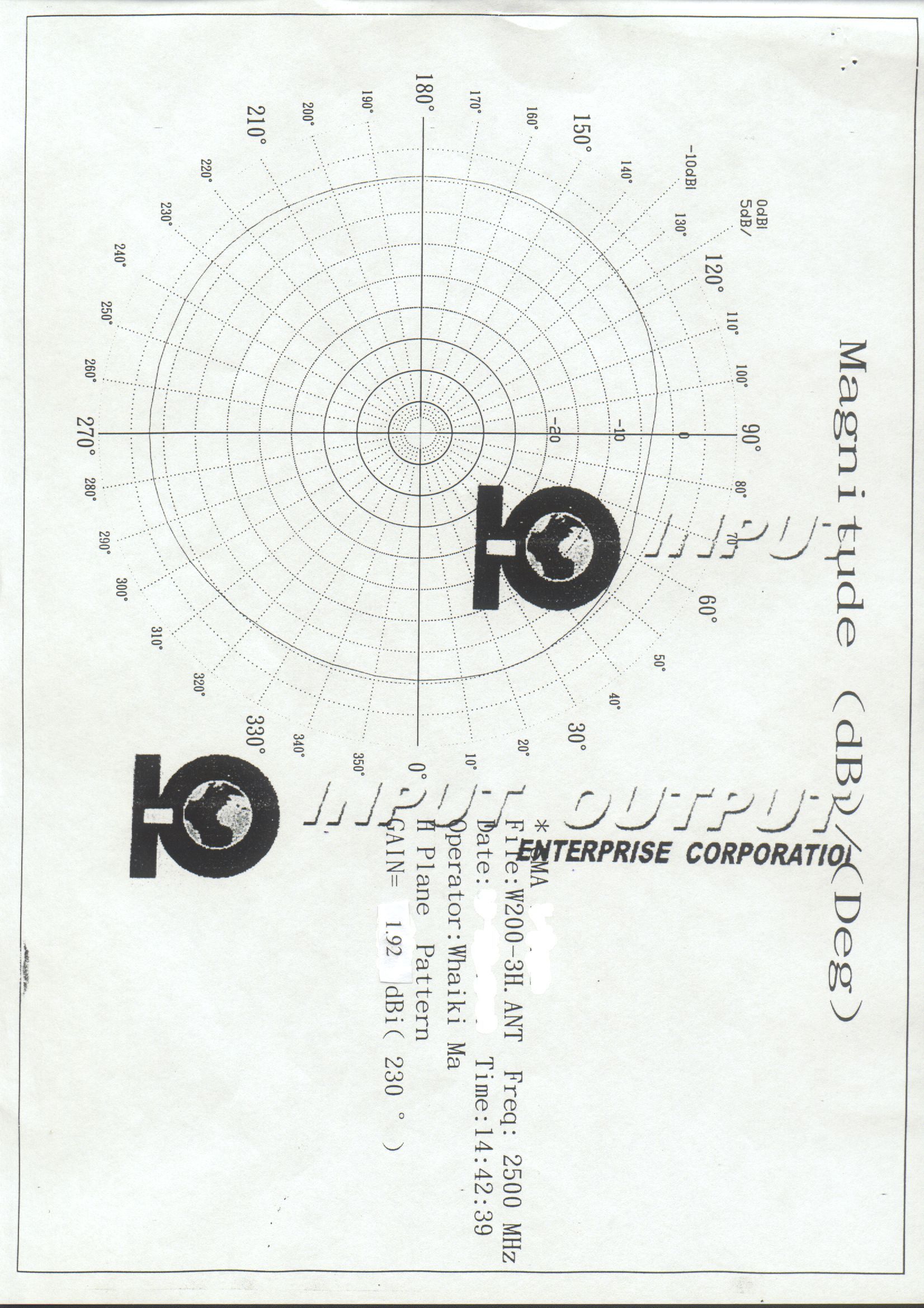
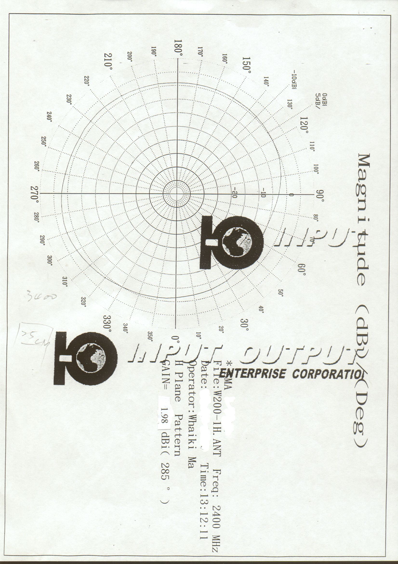
1 Asustek L5H Project Free space gain Report Reported by: Dr. Cliff Wang C.P Liang YM Shen Date: Apr. 10, 2003 PHYCOMP Dual Band Wireless LAN Antenna 1. Antenna Dimension PCB Thickness 0.4mm L5H Right (Main) Antenna L5H Left (Aux) Antenna Right (Main) Antenna Left (Aux) Antenna Antenna Substance 2. Frees pace Frequency response IEEE 802.11 b (2.4~2.5GHz) + 11a (5.15~5.35GHz) Dual Band -Right (Main) Antenna with 192mm cable length 2. Free Space Frequency response -Left (Aux) Antenna with 459mm cable length IEEE 802.11 b (2.4~2.5GHz) + 11a (5.15~5.35GHz) Dual Band 3. Radiation Pattern Measurement Standard Horn Antenna Standard Horn Antenna Measurement Measurement Notebook -The Anechoic Chamber - - 270 270 - - 180 180 - - 90 90 0 0 Direction Definition Direction Definition Antenna 3. Free Space Radiation Pattern Measurement Horizontal Polarization Horizontal Polarization Vertical Polarization Vertical Polarization Vertical Pol.(max)= -2.6 Vertical Pol.(avg)= -8.1 Horizontal Pol.(max)= -1.3 Horizontal Pol.(avg)= -7.3 Total Gain(max)= -1.3 Total Gain(avg)= -5.5 -270 -225 -180 -135 -90 -45 0 45 -Right (Main) Antenna with 192mm cable length @2.412GHz 3. Free Space Radiation Pattern Measurement Horizontal Polarization Horizontal Polarization Vertical Polarization Vertical Polarization Vertical Pol.(max)= -2.9 Vertical Pol.(avg)= -8.5 Horizontal Pol.(max)= -1.2 Horizontal Pol.(avg)= -7.7 Total Gain(max)= -1.2 Total Gain(avg)= -5.9 -270 -225 -180 -135 -90 -45 0 45 -Right (Main) Antenna with 192mm cable length @2.437GHz 3. Free Space Radiation Pattern Measurement Horizontal Polarization Horizontal Polarization Vertical Polarization Vertical Polarization Vertical Pol.(max)= -4.6 Vertical Pol.(avg)= -9.7 Horizontal Pol.(max)= -1.6 Horizontal Pol.(avg)= -8.3 Total Gain(max)= -1.6 Total Gain(avg)= -6.8 -270 -225 -180 -135 -90 -45 0 45 -Right (Main) Antenna with 192mm cable length @2.462GHz 3. Free Space Radiation Pattern Measurement Horizontal Polarization Horizontal Polarization Vertical Polarization Vertical Polarization Vertical Pol.(max)= -9.6 Vertical Pol.(avg)= -13.7 Horizontal Pol.(max)= -3.3 Horizontal Pol.(avg)= -10.2 Total Gain(max)= -3.2 Total Gain(avg)= -9.4 -270 -225 -180 -135 -90 -45 0 45 -Left (Aux) Antenna with 459mm cable length @2.412GHz 3. Free Space Radiation Pattern Measurement Horizontal Polarization Horizontal Polarization Vertical Polarization Vertical Polarization Vertical Pol.(max)= -9.0 Vertical Pol.(avg)= -13.6 Horizontal Pol.(max)= -3.3 Horizontal Pol.(avg)= -10.4 Total Gain(max)= -3.3 Total Gain(avg)= -9.6 -270 -225 -180 -135 -90 -45 0 45 -Left (Aux) Antenna with 459mm cable length @2.437GHz 3. Free Space Radiation Pattern Measurement Horizontal Polarization Horizontal Polarization Vertical Polarization Vertical Polarization Vertical Pol.(max)= -8.7 Vertical Pol.(avg)= -13.3 Horizontal Pol.(max)= -3.5 Horizontal Pol.(avg)= -10.4 Total Gain(max)= -3.4 Total Gain(avg)= -9.5 -270 -225 -180 -135 -90 -45 0 45 -Left (Aux) Antenna with 459mm cable length @2.462GHz
Schematics
123456 A B C D 6 54321 D C B A Title NumberRevisionSize B Date:20-Jan-2003Sheet of File:C:\BCM94301MP_LAYOUT\..\BCM_MiniPCI.schDrawn By: PCI_CBE3_L C3 PCI_CBE2_L G4 PCI_CBE1_L K1 PCI_CBE0_L N1 PCI_FRAME_L G3 PCI_IRDY_L G1 PCI_TRDY_L H1 PCI_DEVSEL_L H3 PCI_STOP_L J1 PCI_PERR_L J2 PCI_SERR_L J3 PCI_PAR J4 PCI_INT_L M5 PCI_RST_L D5 PCI_CLK C5 PCI_PME_L B6 PCI_IDSEL D1 PCI_REQ_L D4 PCI_GNT_L B5 CSTSCHG A5 PCI_CLKRUN_L G2 BCM4301 BGA196_1MM PCI INTERFACE PCI_AD29 B3 PCI_AD28 A1 PCI_AD27 A2 PCI_AD26 B1 PCI_AD25 C1 PCI_AD24 C2 PCI_AD23 D2 PCI_AD22 E4 PCI_AD21 E3 PCI_AD20 E1 PCI_AD19 E2 PCI_AD18 F4 PCI_AD17 F1 PCI_AD16 F2 PCI_AD15 K2 PCI_AD14 K3 PCI_AD13 K4 PCI_AD12 L1 PCI_AD11 L2 PCI_AD10 L3 PCI_AD9 M1 PCI_AD8 P1 PCI_AD7 N2 PCI_AD6 P3 PCI_AD5 N3 PCI_AD4 M4 PCI_AD3 P4 PCI_AD2 N4 PCI_AD1 P5 PCI_AD0 N5 PCI_AD30 C4 PCI_AD31 A4 U11A BCM4301 ac_reset_l 110 mod_audio_mon 111 audio_gnd 113 sys_audio_out 115 sys_audio_in 116 inta_l 20 reserved 36 reserved 43 reserved 110 reserved 112 3p3vaux 24 rst_l 26 gnt_l 30 gnd 102 pme_l 34 ad30 38 plus33v 88 ad28 42 ad26 44 gnd 114 ad24 46 (plug) conminipci3 plus5v 97 intb_l 17 reserved 22 reserved 93 reserved 98 reserved 21 gnd 27 clk 25 gnd 69 req_l 29 ad31 33 ad29 35 gnd 49 ad27 39 ad25 41 plus33v 19 cbe3_l 45 ad23 47 gnd 50 ad21 51 ad19 53 plus33v 28 ad17 57 cbe2_l 59 gnd 62 irdy_l 61 plus33v 31 devsel_l 72 gnd 55 perr_l 71 plus33v 40 plus5v 18 gnd 23 idsel 48 plus33v 89 ad22 52 ad20 54 gnd 32 ad18 58 ad16 60 frame_l 64 trdy_l 66 gnd 37 stop_l 68 clkrun_l 65 par 56 ad15 76 ad13 78 ad11 80 gnd 83 ad9 84 cbe0_l 86 ad6 90 ad4 92 gnd 101 ad2 94 ad0 96 ac_codecid0_l 108 ac_codecid1_l 109 ring 2 8pmj_1 4 8pmj_2 6 8pmj_4 8 8pmj_5 10 led2_yelp 12 led2_yeln 14 reserved 16 sys_audio_in_gnd 118 audio_gnd 120 mpciact_l 122 3p3vaux 124 serr_l 67 plus33v 63 cbe1_l 73 ad14 75 gnd 74 ad12 79 ad10 81 gnd 77 ad8 85 ad7 87 plus33v 70 ad5 91 ad3 95 gnd 82 ad1 99 acsync 103 m66en 104 ac_sdata_ina 105 ac_sdata_out 106 ac_bit_clk 107 tip 1 8pmj_3 3 8pmj_6 5 8pmj_7 7 8pmj_8 9 led1_grnp 11 led1_grnn 13 chsgnd 15 sys_audio_out_gnd 117 audio_gnd 119 reserved 121 plus5va 123 conn_minipci3 J4 CONN_MINIPCI3 Page 1: MiniPCI Interface Page 2: RF Front End Page 3: Radio/Baseband Page 4: Power/Clocks/Misc. MINIPCI INTERFACE bcm94301mp rev 7.3 4 pci_intl vaux pci_rstl pci_gntl GND pci_pmel pci_ad30 pci3_3 pci_ad28 pci_ad26 GND pci_ad24 pci_idsel pci3_3 pci_ad22 pci_ad20 GND pci_ad18 pci_ad16 pci_framel pci_trdyl GND pci_stopl pci_clkrunl pci_par pci_ad15 pci_ad13 pci_ad11 pci_ad9 GND pci_cbe0l pci_ad6 pci_ad4 GND pci_ad2 pci_ad0 mpci_led1 mpciact_l vaux 12 R26 ZERO mpci_led2 mpci_led0 rf_disable_l 12 R27 1K GND GND GND pci_clk GND pci_reql pci_ad31 pci_ad29 GND pci_ad27 pci_ad25 pci_cbe3l pci_ad23 GND pci_ad21 pci_ad19 pci_ad17 pci_cbe2l GND pci_irdyl pci_devsell GND pci_perrl pci3_3 pci_serrl pci3_3 pci_cbe1l pci_ad14 GND pci_ad12 pci_ad10 GND pci_ad8 pci_ad7 pci_ad5 pci_ad3 GND pci_ad1 pci_ad31 pci_ad30 pci_ad29 pci_ad28 pci_ad27 pci_ad26 pci_ad25 pci_ad24 pci_ad23 pci_ad22 pci_ad21 pci_ad20 pci_ad19 pci_ad18 pci_ad17 pci_ad16 pci_ad15 pci_ad14 pci_ad13 pci_ad12 pci_ad11 pci_ad10 pci_ad9 pci_ad8 pci_ad7 pci_ad6 pci_ad5 pci_ad4 pci_ad3 pci_ad2 pci_ad1 pci_ad0 pci_cbe3l pci_cbe2l pci_cbe1l pci_cbe0l pci_framel pci_irdyl pci_trdyl pci_devsell pci_stopl pci_perrl pci_serrl pci_par pci_intl pci_rstl pci_clk pci_pmel pci_idsel pci_reql pci_gntl pci_clkrunl rf_disable_l (PG 3) pci3_3 pci3_3 mpciact_l (PG 4) pci3_3 pci3_3 1 123456 A B C D 6 54321 D C B A Title NumberRevisionSize B Date:20-Jan-2003Sheet of File:C:\BCM94301MP_LAYOUT\..\BCM_Power supply.schDrawn By: 12 R38 20K 1% 12 R39 20K 1% 12 R40 20K 1% mpci_led0 mpci_led1 mpci_led2 12 R25 0 1 2 C87 10UF 1 2 C89 10UF GPIO0 P14 GPIO1 N14 GPIO2 L14 GPIO3 L13 GPIO4 L12 GPIO5 L11 GPIO6 K14 GPIO7 K13 BOOTROM_SCI C6 BOOTROM_SDA D7 SPROM_CS B7 SPROM_CLK A6 SPROM_DOUT A7 SPROM_DIN C7 EXT_POR_L L6 VDDCORE E7 VDDCORE J5 VDDCORE J9 VDDCORE K8 VDDBUS A3 VDDBUS D3 VDDBUS D6 VDDBUS G5 VDDBUS H6 VDDBUS L4 VDDBUS L5 VDDBUS P2 VDDIO E8 VDDIO E9 VDDIO F6 VDDIO G6 VDDIO G8 VDDIO H9 VDDIO J7 VDDIO K9 VDDIO K10 VDDIO M6 VDDIO M12 VDDIO N10 VESD B4 VESD H2 VESD K6 AVDD C13 AVDD D12 AVDD E11 PLLVDD A11 GND F10 GND B2 GND E5 GND E6 GND E10 GND F3 GND F5 GND F8 GND F14 GND G7 GND G9 GND H4 GND H5 GND H7 GND H8 GND J6 GND J8 GND K5 GND K7 GND M2 GND M3 GND M14 GND P12 AGND A14 AGND B10 AGND D14 PLLGND C10 TEST_VCOI F9 PCMCIA_SEL F7 JTAG_TRST_L M13 JTAG_TDO N12 JTAG_TDI N13 JTAG_TCK P11 JTAG_YMS P13 GPIO8 K12 GPIO9 K11 GPIO10 J11 GPIO11 J10 GPIO12 H10 pll_powerdown G10 BCM4301 BGA196_1MM U11 U11E BCM4301 mpci_led0 mpci_led1 mpci_led2 mpciact_l rf_dis_filt_l tr_sw_tx_pu tr_sw_rx_pu CS 1 SK 2 Di 3 Do 4 Vcc3 8 NC 7 ORG 6 GND 5 FM93C46 U13 FM93C46 TSSOP8 1 2 C85 0.1UF mpci_led0 = WLAN activity mpci_led1 = WLAN Radio state mpci_led2 = generic led BCM4307 POWER, RESET, GPIO, CLKS REGULATORS AND POWER SUPPLY FILTERING bcm94301mp rev 7.3 4 ON_OFF 3 BYPASS 4 2 1 Vout 5 Vin GND U8 LP2985 1 2 C56 0.01UF 1 2 C71 2.2UF 1 2 C57 10UF 1 2 C22 0.01UF 1 2 C39 0.01UF 1 2 C28 0.01UF 1 2 C54 0.01UF 1 2 C18 0.1UF 1 2 C21 1000PF 1 2 C40 0.1UF 1 2 C46 0.01UF 1 2 C47 1000PF 1 2 C48 0.1UF 1 2 C41 0.01UF 1 2 C19 0.01UF 1 2 C8 0.1UF 1 2 C6 0.01UF 1 2 C3 0.01UF BCM2051 BYPASS CAPS 1543433, 35474951533162125, 2630 1 2 C94 0.01UF 1 2 C84 1000PF 1 2 C90 0.1UF 1 2 C78 1000PF 1 2 C91 0.1UF 1 2 C83 0.01UF 1 2 C86 0.1UF BCM4307 VDDBUS BYPASS CAPS A3D3D6G5, H6L4, L5P2 1 2 C66 0.1UF 1 2 C74 0.01UF 1 2 C52 0.1UF 1 2 C73 1000PF 1 2 C62 0.1UF 1 2 C76 0.01UF 1 2 C53 0.1UF BCM4307 VDDIO BYPASS CAPS F6, G6G8, H9J7K9, K10M6M12 1 2 C61 1000PF E8, E9N10 1 2 C58 10UF 1 2 C68 0.1UF 12 L9 0 1 2 C75 10UF 1 2 C67 0.01UF 1 2 C70 0.1UF 1 2 C93 0.1UF 1 2 C69 0.01UF 1 2 C55 0.01UF 1 2 C63 10UF 1 2 C49 0.1UF 1 2 C50 1000PF 1 2 C51 1000PF 1 2 C59 0.1UF 1 2 C60 2.2UF 12 L7 MPZ2012S221A 12 L8 MPZ2012S221A BCM4307 VDDCORE BYPASS CAPSBCM4307 AVDD & PLLVDD BYPASS CAPS E7J5J9, K8C13D12E11 1 2 C82 0.1UF 1 2 C92 1000PF 1 2 C81 0.01UF B4H2K6…
Text truncated - open the document above for the full version.
Test Report
Report No. 034L004FI Page: 1 of 46 Version:1.0 Test Report Product Name : WLAN mini-PCI card Model No.: WL-120 FCC ID.: MSQPCCWL120 Applicant : ASUSTeK COMPUTER INC. Address : 4FL., No, 150, Li-Te Rd., Peitou, Taipei, Taiwan, R.O.C. Date of Receipt : Mar. 31, 2003 Date of Test : Apr. 01, 2003 Report No. : 034L004FI The test results relate only to the samples tested. The test report shall not be reproduced except in full without the written approval of QuieTek Corporation. This report must not be used to claim product endorsement by NVLAP any agency of the U.S. Government Report No. 034L004FI Page: 2 of 46 Version:1.0 Test Report Certification Test Date : Apr. 01, 2003 Report No. : 034L004FI Test Results relate only to the samples tested. The test report shall not be reproduced except in full without the written approval of QuieTek Corporation. This report must not be used to claim product endorsement by NVLAP any agency of the U.S. Government Product Name : WLAN mini-PCI card Applicant : ASUSTeK COMPUTER INC. Address : 4FL., No, 150, Li-Te Rd., Peitou, Taipei, Taiwan, R.O.C. Manufacturer : ASUSTeK COMPUTER INC. Model No. : WL-120 FCC ID. : MSQPCCWL120 Rated Voltage : DC 3.3V Trade Name : ASUS Measurement Standard : FCC Part 15 Subpart C Paragraph 15.247 Measurement Procedure : ANSI C63.4: 1992 Test Result : Complied Documented By : ( Chialin Chen ) Tested By : ( Tom Hsieh ) Approved By : ( Gene Chang ) Accredited by NIST (NVLAP) NVLAP Lab Code: 200533-0 Report No. 034L004FI Page: 3 of 46 Version:1.0 TABLE OF CONTENTS Description Page 1. GENERAL INFORMATION .................................................................................................... 5 1.1. EUT Description ........................................................................................................................... 5 1.2. Operational Description ................................................................................................................ 6 1.3. Tested System Datails ................................................................................................................... 7 1.4. Configuration of tested System..................................................................................................... 7 1.5. EUT Exercise Software ................................................................................................................ 8 1.6. Test Facility .................................................................................................................................. 8 2. Conducted Emission ................................................................................................................... 9 2.1. Test Equipment ............................................................................................................................. 9 2.2. Test Setup...................................................................................................................................... 9 2.3. Limits ............................................................................................................................................ 9 2.4. Test Procedure............................................................................................................................. 10 2.5. Test Result of Conducted Emission ............................................................................................ 11 3. Peak Power Output................................................................................................................... 13 3.1. Test Equipment ........................................................................................................................... 13 3.2. Test Setup.................................................................................................................................... 13 3.3. Limits .......................................................................................................................................... 13 3.4. Test Result of Peak Power Output .............................................................................................. 14 4. RF Exposure Evaluation ..........................................................................................................15 4.1. Limits .......................................................................................................................................... 15 4.2. Test Procedure............................................................................................................................. 15 4.3. Test Result of RF Exposure Evaluation ...................................................................................... 16 5. Radiated Emission .................................................................................................................... 17 5.1. Test Equipment ........................................................................................................................... 17 5.2. Test Setup.................................................................................................................................... 17 5.3. Limits .......................................................................................................................................... 18 5.4. Test Procedure............................................................................................................................. 19 5.5. Test Result of Radiated Emission ...............................................................................................20 6. Band Edge.................................................................................................................................. 32 6.1. Test Equipment ........................................................................................................................... 32 6.2. Test Setup.....................................................................................…
Text truncated - open the document above for the full version.
Test Setup Photos
Report No.: 034L004FI Page: 1 of 3 Version:1.0 Attachment 1: EUT Test Setup Photographs Front View of Radiated Test (Mode 1) Back View of Radiated Test (Mode 1) Report No.: 034L004FI Page: 2 of 3 Version:1.0 Front View of Radiated Test (Mode 2) Back View of Radiated Test (Mode 2) Report No.: 034L004FI Page: 3 of 3 Version:1.0 Front View of Radiated Test (Horn)(Mode 1) Front View of Radiated Test (Horn)(Mode 2)
Test Setup Photos
Report No.: 034L004FI Page: 1 of 4 Version:1.0 Attachment 1: EUT Test Setup Photographs Front View of Conducted Test (Mode 1) Back View of Conducted Test (Mode 1) Report No.: 034L004FI Page: 2 of 4 Version:1.0 Front View of Radiated Test (Mode 1) Back View of Radiated Test (Mode 1) Report No.: 034L004FI Page: 3 of 4 Version:1.0 Front View of Radiated Test (Mode 2) Back View of Radiated Test (Mode 2) Report No.: 034L004FI Page: 4 of 4 Version:1.0 Front View of Radiated Test (Horn)(Mode 1) Front View of Radiated Test (Horn)(Mode 2)
Contact Information
Applicant
Jackson Yen(Associate Vice President)
Test Firm
DEKRA Testing and Certification Co., Ltd.Sky Hsu
Technical Specifications
| # | Rule Parts | Frequency Range | Power Output |
|---|---|---|---|
| 1 | 15C | 2.41 GHz - 2.46 GHz | 111.00 mW |
Other Applications from ASUSTeK Computer Inc
MSQ-GC701
Aug 21, 2026Wireless Gaming Controller
Equipment Class
DSS - Part 15 Spread Spectrum TransmitterMSQMPDONGLE3
Aug 18, 2026WIRELESS DONGLE
Equipment Class
DTS - Digital Transmission System
MSQ-GC701D
Aug 13, 2026USB Wireless Dongle
Equipment Class
DSS - Part 15 Spread Spectrum TransmitterMSQ-CM3206DM4A
May 27, 2026Chromebook/Notebook PC
Equipment Class
DCD - Part 15 Low Power Transmitter Below 1705 kHz
MSQ-GST868003
Apr 03, 2026MODULE-WIRELESS CHRG
Equipment Class
DCD - Part 15 Low Power Transmitter Below 1705 kHz