MSQV66GSM Cellphone
ASUSTeK Computer Inc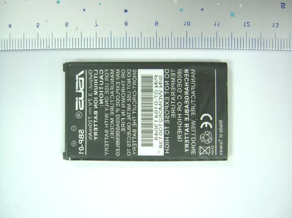
Click to zoom
Application Details
- Equipment Class
- JBP - Part 15 Class B Computing Device Peripheral
- Date of Grant
- Jul 13, 2005
- Application Purpose
- Original Equipment
- Date of Application
- Jul 13, 2005
- Equipment Note
- GSM Cellphone
- Company
- ASUSTeK Computer Inc
- Country
- Taiwan
Documents & Files
Document Text
Text extracted from the exhibit documents filed with the FCC. Open a document above to read the original.
Users Manual
Asus V66 User Manual Contents Welcome5 Left View6 Package Contents6 Overview7 Features7 Specifications9 Menu Map9 Inserting the SIM card, mini SD card, and battery11 Getting Started11 Charging the battery12 Low Battery Indicators12 Turning the phone on/off13 Function Keys13 Unlocking the keypad14 Standby Mode15 Using the Menu16 Text Entry17 Basics17 Choosing text entry methods 18 Calls20 Making a call20 Making International Calls20 Answering a Call20 Answer Mode20 Canceling an Incoming Call21 Diverting a Call21 Redialing a Number21 Call Logs21 Returning a Missed Call21 Call Log Options22 Deleting Call Logs22 Call Time/Cost22 Options During a Call23 Other call options23 Adding Contacts24 Adding a New Entry24 Phonebook24 Searching for a Contact24 Quick Search24 Search Entry24 Copying and Moving25 Deleting Contacts25 Caller Groups26 Extra Number27 Phonebook Settings27 My vCard28 SMS29 Composing an SMS Message 29 Messages29 Common Words30 Message Settings30 SMS Counter31 MMS31 Writing an MMS Message31 Viewing an MMS Message32 Using Templates32 Message Settings32 Chat33 E-mail33 Voice Mail34 Broadcast Message34 Preferred Input34 Settings35 Manner35 Manner Settings35 Phone Settings35 Shortcuts35 Themes36 Phone36 Time and date36 Handset Timer36 Language37 Preferred Input Method37 Default Encoding Type37 Display Settings37 Greeting Text37 Speed Dial37 Arrow Key Settings37 Auto Update of Date and Time 38 Call Settings38 Hide My Number38 Call Waiting38 Call Forwarding39 Call Barring39 Line Switching39 Call Time Reminder39 Call Time Display40 Auto Redial40 Closed User Group40 Call Filter40 Network Settings41 Network Selection41 Preferred Network41 Band Selection41 GPRS Connection41 Security Settings42 SIM Lock42 Phone Lock Code42 Auto Keypad Lock42 Fixed Dialing42 Barred Dialing42 Change Password43 Factory Settings43 Taking Photos44 Camera44 Zoom Function44 Viewing and Managing Photos44 Photo Capture Settings45 Camera Settings45 Image Settings45 Effect46 Add Frame46 Multi-Capture46 Capture Timer46 Default Storage46 Restore Default47 Recording Videos47 Zoom Function47 Viewing and Managing Videos47 Full-Screen Mode48 Rewind and Fast Forward48 Video Playback Speed48 Volume48 Capturing a Still Photo48 Video Capture Settings48 CamcorderSettings48 Video Settings49 Effect49 CamcorderSettings49 Default Storage49 Restore Default50 Media Center51 Audio Player51 Adding music files51 Editing Music Files51 FM Radio52 FM Radio Options52 Java53 Java Settings53 Games54 Game Setting54 Melody Composer54 File Manager55 Organizer55 Viewing drive contents55 Alarm56 Calendar56 Tasks List56 Calculator57 World Clock57 Sound Recorder57 Image editor58 Stopwatch58 Units Converter58 Currency Converter58 Health Manager59 Service Provider Settings60 WAP60 Network60 Browsing WAP pages60 Scrolling60 Viewing Links60 WAP Settings60 Data Account61 Appendix62 Additional Information62 FCC Regulations62 European Notice62 RF Exposure Information (SAR)63 Proper Disposal64 5 Welcome Welcome Congratulations on your purchase of an Asus V66 cell phone. The following illustration displays the features found on the front of your phone. Speaker Screen Up joystick key: Displays the SMS inbox; scrolls up through menu items Right soft key: Displays phone book when idle; selects right menu items Power/end key: Turns power on or off; ends a call; exits menu Right joystick key: Displays the Media Center menu; scrolls right through menu items Down joystick key: Displays your shortcuts menu; scrolls down through menu items Left soft key: Displays the main menu; selects left menu items Call key: Answers a call; displays previously dialed numbers Left joystick key: Displays the camera menu; scrolls left through menu items Enter key: Displays the main menu; confirms selection of a menu item Joystick: Includes up, down, right, left keys for on-screen navigation 6 Left ViewPackage Contents warranty card User Manual Quick Start Guide V66 handset720 mAh Li-ion battery Travel charger Stereo headsetMini-SD card Accessory chain Handset Manager manual Warranty card User manual Quick start guide Handset Manager CD-ROM Captures photos Increases or decreases the volume for calls, key tones, or playing media files. USB cable Handset Manager Manual 7 Welcome Overview The V66 is a stylish and fashionable new phone from Asus, with all the functions and utilities to make it a useful tool in today’s mobile world. The V66 comes equipped with a built-in camera, MMS/SMS messaging capability, organizer, java games, audio player, WAP, GPRS, and a mini SD card slot. In addition to the internal 30 MB phone memory, the mini SD card provides additional memory where you can store your contact information, messages, text, graphics, and audio files. The V66’s audio player enables you to play back your favorite music. Features • Wide variety of calling and messaging functions • Built-in camera • Media center with audio player, FM radio receiver, and games for your entertainment • MMS and SMS messaging capability • Personal information organizer with alarm, calendar, calculator and other useful tools to manage your time • WAP and GPRS capability to check e-mail or browse web services 8 Specifications System supportedGSM900/1800/1900, Class 10 Size99.8 x 43.8 x 18.7 mm Weight90g Battery720 mAh Li-ion Standby Time200 ~ 300 hours Talk Time2.5 ~ 4 hours ColorSilver, Orange, Blue Display1.8-inch, 256K colors, TFT, 128 x 160 Camera300K pixel CMOS Supports video recording 4/6/9/16 continuous shots WAPSupports WAP 1.2.1 and WAP 2.0 JavaSupports J2ME (CLDC + MiDP 1.0.3) Built-in Java games MessagingSupports SMS, EMS, MMS Ring tone64 polyphonic ring tones Supports SMF (standard MIDI format) and MP3 Phone book300 sets + SIM card Caller ID with photos 10 sets for speed dialing 10 sets for voice messaging RecordRecord an unlimited number of files, up to memory capacity Calendar10 sets Internal Memory30 MB External storageMini-SD card PIM toolAlarm, calculator, worldwide clock, calendar, note, curre…
Text truncated - open the document above for the full version.
Cover Letter(s)
ASUSTeK COMPUTER INC. No. 150, Li-Te Rd., Peitou, Taipei, Taiwan R.O.C. Tel:886-2-28943447 Fax:886-2-28907699 June 20,2005 Power Of Attorney To whom it may concern, Please be notified that we, ASUSTek Computer Inc., the undersigned, hereby authorize A Test Lab. Corp. Ltd., located at No. 17 Lane 772 Ho-Ping Rd., Pa-Te city Taoyuan Taiwan R.O.C. to act on our behalf in all matters relating to all processes related to FCC applications and communications issue. Any and all acts carried out by A Test Lab. Corp. Ltd. On our behalf shall have the same effects as acts of our own. This authorization is limited to the product of as following : 1. Multimedia mobile phone : ASUS V66 (MSQV66) Any acknowledgement and response, please send it to A Test Lab. Techno. Corp. Ltd. Directly. If you have any questions regarding this authorization, please feel free to contact us. Sincerely, ___________________________ MF Chen Engineer ASUSTeK Computer INC. No. 150, Li-Te Rd., Peitou, Taipei, Taiwan R.O.C. Tel:886-2-28943447 Fax:886-2-28907699
Cover Letter(s)
American Telecommunications Certification Body Inc. 6731 Whittier Ave, McLean, VA 22101 June 26, 2005 RE: ASUSTek Computer Inc. FCC ID: MSQV66 After a review of the submitted information, I have a few comments on the above referenced Application. 1) Please correct the various items on the 731 form: a) Section I - 3(a) and 3(b) must list the FCC ID to be Certified. Please correct. b) Section II - Please fill in correct address for ATL or the appropriate company in section 2(a). c) Section III - Section 6 of the 731 form must be filled in for (a)(b)(c)(d). For Part 22, (a) would be listed for ERP. For Part 24, (b) would be listed as EIRP. Additionally, please fill in Section 4(a)/(b), 7, 8, or 9. d) Section IV must be filled in as appropriate. 2) Confidentiality is given under section 0.456 and 0.459 of the FCC rules, not Part 15 and 24. Please correct the confidentiality letter as appropriate. 3) The block diagram should include the block diagram of the RF portion of the device. Please update/provide as necessary. 4) It appears that complete internal photographs have not been provided. The top and bottom of all boards must be provided. Additionally, photographs showing beneath all subshields should also be provided. Please provide. 5) It would be recommended that the operational description and BOM also be added to the confidentiality letter. If this is desirable, please provide an updated confidentiality letter that included these items. 6) The parts list appears incomplete and only lists some of the RF components. Please provide a complete parts list. 7) The schematics appears to contain most of the RF portion of the device, but appears to be incomplete through to the baseband portion of the device. Please provide further schematics as necessary. 8) For the tune up procedure by the manufacturer, please explain whether power is measured radiated or conducted. It is hard to achieve the necessary accuracy if this is measured in a radiated fashion. Please explain. 9) Please provide a separate test configuration photographs exhibit. --- Continued on Next Page --- z Page 2 June 30, 2005 10) This device is capable of connection to a PC and is therefore also considered a PC peripheral device (in addition to the TX requirements, i.e. Part 24, etc.) and is subject to either a Certification or DoC as a PC peripheral. Therefore the application must clarify if you are asking for: a) Certification of the device as a TX, and a DoC has been performed by an appropriately accredited test lab for a PC peripheral b) Certification as a TX + PC peripheral. Note 1: The option b) would be considered as a composite application and 2 certificates (one for the TX, one for the PC peripheral portion) would be issued. Note that there are additional review costs associated with this additional certification. Note 2: To qualify to perform DoC applications, the test lab must be accredited (i.e. NVLAP or A2LA) to perform testing under the DoC procedure. Note 3: Note that for DoC tests, the device is configured with a minimum test configuration as specified by ANSI C63.4 which includes complete computer + 2 I/O devices attached (one may be the EUT) during this particular test. Information appears to be provided that supports this. Note 4: Each path (DoC or Certificaiton) has particular labeling requirements that must be followed. For DoC authorizations, the label should also include specific DoC labeling information and also the users manual should include information regarding Part 2.1077. If the device is Certified, the FCC ID and current labeling requirements for the TX will cover the labeling requirements. However, additional grants are generated and review costs are higher. Currently labeling and users manual DO NOT support a DoC Authorization. The manufacturer does have a choice of DoC or Certification, however the device labeling must match the appropriate methods used. 11) If this device is being approved under a DoC, then all the information required by 2.1077 must be placed on a single page in the users manual. 12) FCC ID specified within the users manual does not match this application. Please correct. 13) Page 66 of the users manual mentions a 20 cm spacing which is not applicable to this device and should be removed. Please correct. Part 24 Review 14) Please provide both the DC voltages and currents applied into the several elements of the final radio frequency amplifying device for normal operation over the power range. If this is already in the application, kindly point to where this information may be found. 15) Minimum Passing Margin on page 5 of the Part 24 report does not appear correct. Please review. 16) ANSI C63.4 does not actually apply to the Part 24 report. Appropriate standards should be listed as EIA/TIA 603 standards. Please review/correct as necessary. 17) Where possible, the conducted power should also be measured and documented in the Part 24 report. Please provide. 18) Please explain the column “EUT Power Value” on page 10 of the Part 24 report. This column does not appear to be conducted power and other possible uses for this column do not appear to fit the data provided. Please explain as necessary. 19) On page 13 of the Part 24 report, some correction factors are negative, others are positive. It is believed that all of these should all be the same sign. Please review. 20) The plots on page 16, 19, and 22 do not appear to show a high fundamental carrier as expected (i.e. close to 29.2 dBm as specified by the tune up procedure). Note it appears that z Page 3 June 30, 2005 the sweep time may have been inadequate (too fast) to adequately capture the emissions. Please review/correct/or explain as necessary. 21) For frequency stability tests, please confirm that the device was soaked between temperature settings of adequate time to stabilize both the device and chamber. A soak time (after chamber reaches appropriate temperature) of 1 hours is considered normal. 22) Page 22 appears to shows s…
Text truncated - open the document above for the full version.
Cover Letter(s)
Reply for ATCB Comments of 062605b 1) Please correct the various items on the 731 form: a) Section I - 3(a) and 3(b) must list the FCC ID to be Certified. Please correct. b) Section II - Please fill in correct address for ATL or the appropriate company in section 2(a). c) Section III - Section 6 of the 731 form must be filled in for (a)(b)(c)(d). For Part 22, (a) would be listed for ERP. For Part 24, (b) would be listed as EIRP. Additionally, please fill in Section 4(a)/(b), 7, 8, or 9. d) Section IV must be filled in as appropriate. - 06/30/2005 upload new 731 form 2) Confidentiality is given under section 0.456 and 0.459 of the FCC rules, not Part 15 and 24. Please correct the confidentiality letter as appropriate. - will upload new file soon. 3) The block diagram should include the block diagram of the RF portion of the device. Please update/provide as necessary. - 06/30/2005 upload new diagram 4) It appears that complete internal photographs have not been provided. The top and bottom of all boards must be provided. Additionally, photographs showing beneath all subshields should also be provided. Please provide. - uploaded 5) It would be recommended that the operational description and BOM also be added to the confidentiality letter. If this is desirable, please provide an updated confidentiality letter that included these items. - we had revise the confidential request and put part list(BOM),Tune up procedure....etc on it. 6) The parts list appears incomplete and only lists some of the RF components. Please provide a complete parts list. - 06/30/2005 upload new BOM 7) The schematics appears to contain most of the RF portion of the device, but appears to be incomplete through to the baseband portion of the device. Please provide further schematics as necessary. - 06/30/2005 upload new diagram 8) For the tune up procedure by the manufacturer, please explain whether power is measured radiated or conducted. It is hard to achieve the necessary accuracy if this is measured in a radiated fashion. Please explain. - Conducted 9) Please provide a separate test configuration photographs exhibit. - uploaded 10) This device is capable of connection to a PC and is therefore also considered a PC peripheral device (in addition to the TX requirements, i.e. Part 24, etc.) and is subject to either a Certification or DoC as a PC peripheral. Therefore the application must clarify if you are asking for: a) Certification of the device as a TX, and a DoC has been performed by an appropriately accredited test lab for a PC peripheral b) Certification as a TX + PC peripheral. Note 1: The option b) would be considered as a composite application and 2 certificates (one for the TX, one for the PC peripheral portion) would be issued. Note that there are additional review costs associated with this additional certification. Note 2: To qualify to perform DoC applications, the test lab must be accredited (i.e. NVLAP or A2LA) to perform testing under the DoC procedure. Note 3: Note that for DoC tests, the device is configured with a minimum test configuration as specified by ANSI C63.4 which includes complete computer + 2 I/O devices attached (one may be the EUT) during this particular test. Information appears to be provided that supports this. Note 4: Each path (DoC or Certificaiton) has particular labeling requirements that must be followed. For DoC authorizations, the label should also include specific DoC labeling information and also the users manual should include information regarding Part 2.1077. If the device is Certified, the FCC ID and current labeling requirements for the TX will cover the labeling requirements. However, additional grants are generated and review costs are higher. Currently labeling and users manual DO NOT support a DoC Authorization. The manufacturer does have a choice of DoC or Certification, however the device labeling must match the appropriate methods used. 11) If this device is being approved under a DoC, then all the information required by 2.1077 must be placed on a single page in the users manual. - 15B will be certify not DoC 12) FCC ID specified within the users manual does not match this application. Please correct. 13) Page 66 of the users manual mentions a 20 cm spacing which is not applicable to this device and should be removed. Please correct. - will uploaded soon 14) Please provide both the DC voltages and currents applied into the several elements of the final radio frequency amplifying device for normal operation over the power range. If this is already in the application, kindly point to where this information may be found. Please reference to Sec.4 point.1 15) Minimum Passing Margin on page 5 of the Part 24 report does not appear correct. Please review. We corrected 16) ANSI C63.4 does not actually apply to the Part 24 report. Appropriate standards should be listed as EIA/TIA 603 standards. Please review/correct as necessary. We corrected 17) Where possible, the conducted power should also be measured and documented in the Part 24 report. Please provide. Please reference to 4.1 page7 18) Please explain the column “EUT Power Value” on page 10 of the Part 24 report. This column does not appear to be conducted power and other possible uses for this column do not appear to fit the data provided. Please explain as necessary. EUT Power Value: 1. It means when we put EUT on Chamber that is connected to Base Station, and we receiver value and record from Spectrum. That value is “EUT Power Value” 2. Next, we change EUT to Substitution Antenna, and feeding power from SG. More detail, please find 6.2(b) 19) On page 13 of the Part 24 report, some correction factors are negative, others are positive. It is believed that all of these should all be the same sign. Please review. We corrected 20) The plots on page 16, 19, and 22 do not appear to show a high fundamental carrier as expected (i.e. close to 29.2 dBm as specified by the tune up procedure). Note it appears that the sweep t…
Text truncated - open the document above for the full version.
Cover Letter(s)
27) The tune up mentions 29.2 dBm (840 mW), while the maximum power measured in the Part 24 report was 740 mW. Please explain. Sorry, is mistake. 29dBm is 794mW on SAR report. For SAR report, 29.0dBm (794mW) is conducted output power, is same as FCC part 24 4.1(P7) output power 28.9dBm (780mW). And, 740mW is for Max EIRP. 28) The SAR report page 3 mentions a 29 dBm conducted measurement which equals 794 mW. However the power listed next to this cites 870 mW. Please explain the difference. What was measured? Sorry, is mistake. 29dBm is 794mW. Additionally, please note that conducted measurements should also have been performed and shown in the Part 24 report. The FCC asks that we review power cited in the theory of operation, tune up procedure, EMC report and SAR report. Additionally, they require that a) Powers in SAR report must agree with EMC report and tune-up procedure and b) Conducted power in SAR report should be greater than or equal to what’s in EMC report, but not exceeding tune-up/tolerance. If conducted powers are not shown in the Part 24 report as well, this can not adequately be determined. Also note that power measurements cited in the theory and SAR report appear somewhat inconsistent. Please review/correct as necessary. Understand! we will attention. 29) Please provide a list of any manufacturer body worn supplied accessories for this device (holsters, etc.). Additionally, please explain if there are there any manufacturer offered accessories for use with this device which may affect SAR (battery options, etc.). Please explain. Please reference to Fig.16, 17, 18, and table supplied accessories is earphone. So, our testing is including earphone. 30) The statement of compliance on the bottom of page 3 of the SAR report should also cite compliance with FCC RF exposure requirements as required by §2.1093. OK. We corrected. 31) When information reported in the users manual reports SAR values, it should match the SAR values measured. Please correct the users manual to report the correct SAR values. OK. 32) Liquid parameters must be measured each day of testing as a minimum, or more were high conditions of evaporation or low humidity exist. It appears that parameters were only measured on October 2004. Sorry, is mistake. We corrected. 33) FYI ....Page 18 and Table 2 only appear to mention an 1800 MHz dipole. Although in the past the FCC has stated verification frequency(s) must be within ± 100 MHz of device center frequency(s), most actually provide this at 1900. It is recommended to use this for future applications. Understand! 34) The report only mentions 1800 MHz Validation equipment, but it appears the validation was done at 1900 MHz. Note this would not be allowed as the resonance of the equipment at the different frequencies is unknown, expected values are for correct dipole and medium, etc. Note the paragraph on page 19 mentions 1800. However the data tables on page 19 and plots support 1900 MHz using 1800 MHz equipment. That is our misunderstanding and mistake. So, combine question 33 and 34, we should have 1900MHz validation Kit that will be better. Or, we can still use 1800MHz validation Kit, but also calibrate at 1800MHz. On our testing data, that is testing on 1900MHz. We will change our testing SOP to 1800MHz.Can we change procedure on next time? 35) In the future, please consider placing larger test configuration photographs (1-2 per page) in the report. The current photographs are smaller than desired. OK, we will attention. 36) Some SAR plots show secondary hot spots. In these cases, both hot spots should be checked to ensure worse case was measured. Because in DASY’s setting, if second hot point is small than first hot point 0.2dB and max value small than 0.5, than SAR plot will appear first hot point only. 37) Liquid parameters given on SAR plots do not appear to match information in previous tables regarding liquid parameters measured. Please review. Additionally, these parameters should have been measured the day of test. It does not appear this was the case. Sorry, is mistake. We corrected. 38) The FCC asks that Ambient and liquid temperatures be placed on all plots. This does not appear to have been done. Please reference 10.1(p24) and 10.5(p26), we have show on Table already. 39) Test Report should document: a) report probe tip distance to phantom inner surface b) that the distance between the measurement point (distance + offset) at the probe sensor location (geometric center behind the probe tip) and the phantom surface is < 8.0 mm and maintained at a constant distance of +/- 1.0 mm during an area scan to determine peak SAR locations c) if probe boundary effect compensation is used or not. If not the probe tip should be positioned at least half a probe tip diameter from the phantom surface during area and zoom scans. Please reference to 5.1.1 page7, which include some probe information (Distance from probe tip to dipole centers: 2.7mm)
Cover Letter(s)
American Telecommunications Certification Body Inc. 6731 Whittier Ave, McLean, VA 22101 July 5, 2005 RE: ASUSTek Computer Inc. FCC ID: MSQV66 After a review of the submitted information, I have a few comments on the above referenced Application. Note: We show that many uploads were tried but rejected by our server. Note that our system rejects file names of the same name if they are upload more than once. Therefore each new revised exhibit should be renamed with an extension that denotes it is new such as “rev 1”, “revised 070105”, etc. We show we only received the following documents since 6/27/05: Confidential_V66 circuit diagram.pdf Confidential_V66 RF circuit Block diagram.pdf 05-0368-E-00-02-01 ASUS V66_20050628.pdf 05-0368-SEO ASUS V66_test configuration photographs.pdf and via email, 2 sets of responses and an updated SAR report. 1) New 731 form for previous item 1 does not appear to have been received. Please provide. This should have addressed the following issues. a) Section I - 3(a) and 3(b) must list the FCC ID to be Certified. Please correct. b) Section II - Please fill in correct address for ATL or the appropriate company in section 2(a). c) Section III - Section 6 of the 731 form must be filled in for (a)(b)(c)(d). For Part 22, (a) would be listed for ERP. For Part 24, (b) would be listed as EIRP. Additionally, please fill in Section 4(a)/(b), 7, 8, or 9. d) Section IV must be filled in as appropriate. 2) New confidentiality letter not yet received for previous item 2. Please provide. This should have addressed the following issues: Confidentiality is given under section 0.456 and 0.459 of the FCC rules, not Part 15 and 24. Please correct the confidentiality letter as appropriate. 3) The RF block diagram should show the frequencies of all oscillators in the TX device (CFR 2.1033(a)(5)). Since this device is also being certified as a PC peripheral device, the main host block diagram should also include oscillator information. Please correct. 4) New internal photos for previous item 4 does not appear to have been received. This should have addressed the following issues: It appears that complete internal photographs have not been provided. The top and bottom of all boards must be provided. Additionally, photographs showing beneath all subshields should also be provided. Please provide. 5) New confidentiality letter for previous item 5 does not appear to have been received. This should have addressed the following issues: It would be recommended that the operational description and BOM also be added to the confidentiality letter. If this is desirable, please provide an updated confidentiality letter that included these items. 6) New BOM for previous item 6 does not appear to have been received. This should have addressed the following issues: The parts list appears incomplete and only lists some of the RF components. Please provide a complete parts list. --- Continued on Next Page --- z Page 2 July 5, 2005 7) New users manual for previous item 12 & 13 does not appear to have been received. This should have addressed the following issues: a) FCC ID specified within the users manual does not match this application. Please correct. b) Page 66 of the users manual mentions a 20 cm spacing which is not applicable to this device and should be removed. Please correct. Part 24 Review 8) Your response to previous question 14 references currents/voltages that are ratings of the device. The FCC is concerned with the DC voltages and currents applied into the several elements of the final radio frequency amplifying device for normal operation over the power range. This is typically different than the devices ratings and will likely need to come from the manufacturer. Please provide. 9) Minimum Passing Margin for power on page 5 of the Part 24 report does not appear to be stated correctly. Please review. 10) A response to previous question 20 does not appear to have been provided. Please provide. This should have addressed the following issues: The plots on page 16, 19, and 22 do not appear to show a high fundamental carrier as expected (i.e. close to 29.2 dBm as specified by the tune up procedure). Note it appears that the sweep time may have been inadequate (too fast) to adequately capture the emissions. Please review/correct/or explain as necessary. 11) Page 22 appears to shows some other spurs of interest other than the fundamental and base station that were not reported and are higher than the reported values. Please review and/or explain as necessary.. 12) 99% power bandwidth does not appear to be measured based upon below the transmitter power (maximum conducted power – 29.1 dBm as specified in tune up procedure). I have attached an document that helps explain this testing better. In short, the 26 dB down from the reference level should be measured....This usually gives something near 250 kHz. 13) While you explained for previous question 24 the loss of cable and splitter to be 4.5 dB, it is uncertain if the cable loss and power divider loss were factored into the plots of page 45 and 46. Please explain. SAR Review 14) New users manual for previous item 31 does not appear to have been received. This should have addressed the following issues: a) When information reported in the users manual reports SAR values, it should match the SAR values measured. Please correct the users manual to report the correct SAR values. 15) Because of the issue involved with using the 1800 MHz dipole with an injection frequency of 1900 and 1900 MHz fluid, a retest per our discussions today will be necessary for a minimum of the worse 2 case points previously measured. If data is similar, then we will accept the data as correct. If the data is found to be significantly different, then an entire retest will be required. 16) FYI...please note that many times we have seen the FCC ask that tissue parameters be measured across the band and not just at the center frequencies. Please take this into consideration …
Text truncated - open the document above for the full version.
Cover Letter(s)
8) …
Text truncated - open the document above for the full version.
Contact Information
Applicant
Jackson Yen(Associate Vice President)
Technical Contact
Non-Technical Contact
ATLSophia Lu
[email protected]886-2-82122828
Test Firm
BTL Inc.Andy Chiu
Technical Specifications
| # | Rule Parts | Frequency Range | Power Output |
|---|---|---|---|
| 1 | 15B | - | - |
Other Applications from ASUSTeK Computer Inc
MSQ-GC701
Aug 21, 2026Wireless Gaming Controller
Equipment Class
DSS - Part 15 Spread Spectrum TransmitterMSQMPDONGLE3
Aug 18, 2026WIRELESS DONGLE
Equipment Class
DTS - Digital Transmission System
MSQ-GC701D
Aug 13, 2026USB Wireless Dongle
Equipment Class
DSS - Part 15 Spread Spectrum TransmitterMSQ-CM3206DM4A
May 27, 2026Chromebook/Notebook PC
Equipment Class
DCD - Part 15 Low Power Transmitter Below 1705 kHz
MSQ-GST868003
Apr 03, 2026MODULE-WIRELESS CHRG
Equipment Class
DCD - Part 15 Low Power Transmitter Below 1705 kHz