N3ESVC70436TXSpy Video Car
Wild Planet Entertainment, Inc.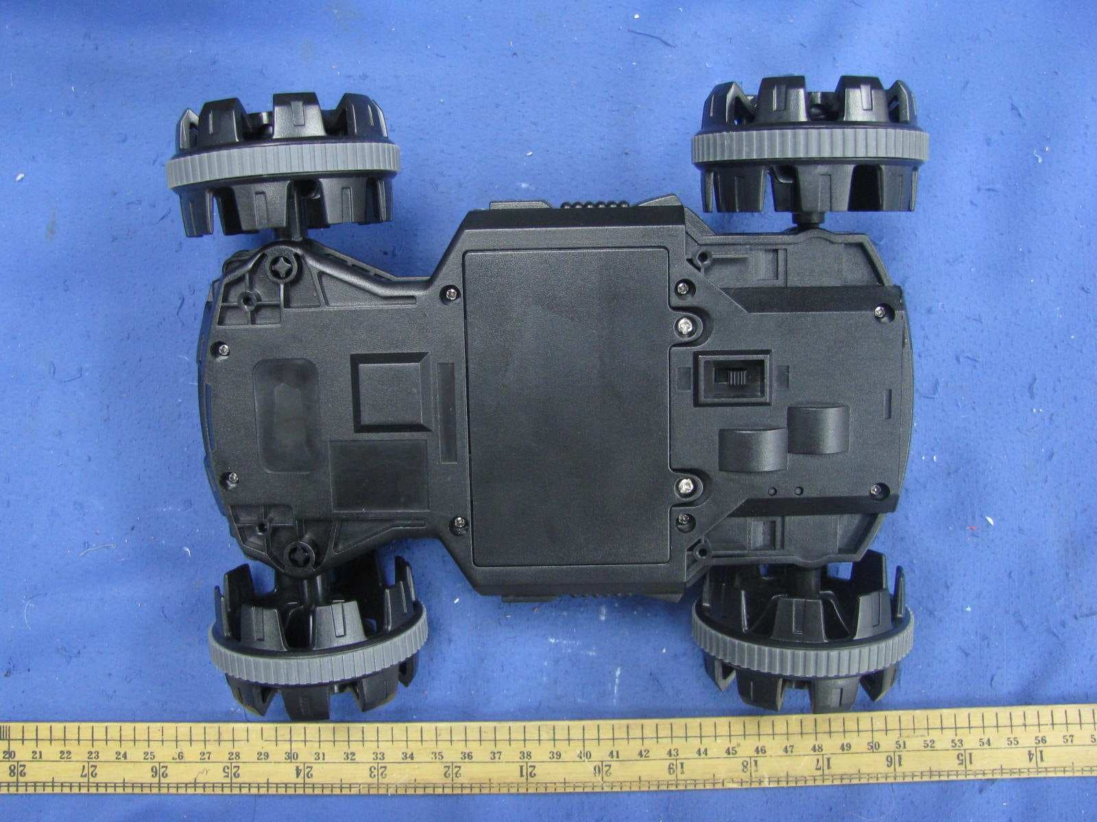
Click to zoom
Application Details
- Equipment Class
- DXX - Part 15 Low Power Communication Device Transmitter
- Date of Grant
- Jun 07, 2011
- Application Purpose
- Original Equipment
- Date of Application
- Jun 07, 2011
- Equipment Note
- Spy Video Car
- Frequency Range
- 2410.87500000 - 2464.87500000
- Country
- United States
Documents & Files
Document Text
Text extracted from the exhibit documents filed with the FCC. Open a document above to read the original.
Users Manual
On/off switch Night vision button (button A ) Color video screen Forward/reverse control Left/right control Front wheel alignment Antenna SPY VIDEO CAR VX6 REMOTE Fig. 2 Fig. 3 Fig. 1 On/off switch IR LED Camera Ages 8 and up 70436 Requires 10 AA batteries (6 for the car and 4 for the remote), not included. Important: Please save this instruction sheet. It contains valuable product information. Spy Gear Consumer Service is ready to assist you! DO NOT RETURN THE PRODUCT TO THE STORE! USE OUR TOLL-FREE CONSUMER HELPLINE 1-800-247-6570 WWW.WILDPLANET.COM/HELP SPY VIDEO CAR VX6 ™ PREPARING TO DRIVE THE SPY VIDEO CAR VX6 1. ADULTS: Install the batteries in the SPY VIDEO CAR VX6 and REMOTE CONTROL (see below for directions). 2. Turn on the Spy Video Car VX6 using the ON/OFF SWITCH located on the bottom of the car between the rear wheels. (Fig.1) 3. Use the ON/OFF SWITCH to turn on the remote control. DRIVING WITH THE REMOTE CONTROL 1. Use the FORWARD/REVERSE CONTROL to drive the car forward and reverse. 2. Use the LEFT/RIGHT CONTROL to turn the car left and right. LEGEND Battery level Signal strength NIGHT VISION Lets you see in the dark without being seen. • Press Button A to toggle the IR LED light on or off. Using the IR LED works great in dark rooms. SAFETY • Don’t drive the Spy Video Car VX6 in sand or through water (even small puddles) or snow. (Fig. 2) • Never drive the Spy Video Car VX6 on real streets. • To avoid damage to the video camera or internal electronics, do not drive the Spy Video Car VX6 off curbs or down stairs. (Fig. 3) • Don’t store the Spy Video Car VX6 near heat or in direct sunlight. • Always turn switches OFF and remove all batteries for storage. • Warning! Use under the direct supervision of an adult. • Keep fingers, hair, and loose clothing away from the tires while the vehicle is switched on. RESET SYNC ATTENTION ADULTS: TO REPLACE BATTERIES The Spy Video Car VX6 requires 10 AA (LR06) batteries (6 for the car and 4 for the remote control), not included. (Fig. 4 & 5) 1. Use a small Phillips head screwdriver to loosen the screws on the battery compartment of both the vehicle and the remote. The screws are attached to the covers. 2. Open battery cover. Remove exhausted batteries. 3. Place new batteries in compartment as shown in the image. 4. Replace the battery cover and tighten screws. BATTERY SAFETY INFORMATION • Only adults should install and replace batteries. • Rechargeable batteries are to be removed from the toy before being charged. • Rechargeable batteries are only to be charged under adult supervision. • Non-rechargeable batteries are not to be recharged. • Remove dead or exhausted batteries. • Insert batteries correctly. Match positive and negative signs. • The supply terminals are not to be short circuited. • Do not mix alkaline, standard (carbon-zinc), or rechargeable (nickel-cadmium) batteries. • Do not mix old and new batteries. • Only the batteries of the same or equivalent type recommended to be used. • Do not dispose batteries in a fire; they may explode. • Dispose of batteries safely. Warning! Changes or modifications to this equipment not expressly approved by the party responsible for compliance could void the user’s authority to operate the equipment. TROUBLESHOOTING GUIDE PROBABLE CAUSE The batteries are dead or have a low charge. The batteries may not be installed correctly. Power switches are OFF. The batteries are dead or have a low charge. The Spy Video Car VX6 signal strength is low. Power switches are OFF. The front wheel alignment may not be set correctly. You are playing near areas with radio interference, other RC vehicles, high-tension wires, large buildings, CB radios. The Spy Video Car VX6 is out of range. The batteries have a low charge. The remote control antenna is not sending clear signals. The Spy Video Car VX6 may be located in direct sunlight. You are playing near an area with radio interference or a cordless phone. SOLUTION Replace the batteries and always remember to turn off the power switches on the car and remote control to save battery life when not in use. Make sure the battery direction (polarity, +/-) is correct. Make sure the power on the remote control and the car is ON. Replace the batteries and always remember to turn off the power switches on the car and remote control to save battery life when not in use. Try holding the remote control higher above the ground. If that does not work, move closer to the car. Make sure the power on the remote control and the car is ON. Adjust the front wheel alignment screw located on the car behind the video camera. If the car turns to the right, turn the screw to the left and vice versa. Move to a new location. Try holding the remote control higher above the ground. If that does not work, move closer to the car. Replace the batteries and always remember to turn off the power switches on the car and remote control to save battery life when not in use. Point the remote control antenna up in the air, not at the car. Do not touch the antenna. Move inside or to a shadier area outside. Move to a new location. SYMPTOM The Spy Video Car VX6 will not operate. The Spy Video Car VX6 slows down or the video screen starts to fade. There is no image on the video screen. The Spy Video Car VX6 is not traveling in a straight line. The Spy Video Car VX6 is moving about erratically, not under the control of the remote. When I look at the video screen, everything looks white. The video screen is flickering a lot. REMOTE ID: N3ESVC70436RX CAR ID: N3ESVC70436TX This device complies with part 15 of the FCC Rules. Operation is subject to the following two conditions: (1) This device may not cause harmful interference, and (2) This device must accept any interference received, including interference that may cause undesired operation. NOTE: This unit has been tested and found to comply with the limits for a Class B digital device, pursuant to Part 15 of the FCC Rules. These limits are designed to provi…
Text truncated - open the document above for the full version.
Block Diagram
Block Diagram RF Module 2410.875-2464.875MHz Oscillator 12MHz Oscillator 18MHz Band pass Filter 2410.875-2464.875MHz
External Photos
External Photos
ID Label/Location Info
Label Artwork and Location FCC ID : N3ESVC70436TX This device complies with Part 15 of the FCC Rules. Operation is subject to the following two conditions: (1) this device may not cause harmful interference, and (2) this device must accept any interference received, including interference that may cause undesired operation.
Internal Photos
Internal Photos
Operational Description
Car unit Technical Description The equipment under test (EUT) is a 2.4GHz transceiver of a Spy Video Car with 17 channels operating at 2410.875-2464.875 MHz MHz. The Spy Video Car has two units, one is the Remote Controller unit, and the other is the Car unit. The Remote Controller unit is powered by 6VDC (4 x 1.5V "AA" batteries) and the Car unit is powered by 9.0VDC (6 x 1.5V "AA" batteries). Channel List: Channel Frequency 0 2410.875 1 2414.250 2 2417.625 3 2421.000 4 2424.375 5 2427.750 6 2431.125 7 2434.500 8 2437.875 9 2441.250 10 2444.625 11 2448.000 12 2451.375 13 2454.750 14 2458.125 15 2461.500 16 2464.875 Modulation Type: GFSK Antenna Type: Integral antenna IC Function and circuit description: Digital Board 1. U4 acts as RF module. 2. U6 acts DC/DC Converter. 3. U2 acts as power regulator. 4. U5 acts as SONiX 8-Bit Micro-Controller. RF Board U4 1. U1 acts as MCU. 2. U2 acts as CMOS Serial Flash. 3. UR2 acts as 2.4GHz TX/RX Chip. 4. UR1 acts as High Speed LDO regulator. 5. UH1 acts as RF power amplifier. 6. SH1 acts as DC-2.5GHz SPDT Switch. 7. LH1 acts as Band pass filter. 8. Y1 acts as oscillator for U1. 9. XR1 acts as oscillator for UR2. The datasheet of the 2.4GHz TX/RX Chip is attached. A7121/A7122 Final Version 2.4GHz GFSK Transceiver Nov. 2010, Version 1.4 (Final Version)1AMICCOM Electronics Corporation Typical Applications n Wireless digital audio n Wireless Mouse and Keyboard n 2.4GHz ISM Band Communication System nWireless game pad nWireless toy General Description A7121/A7122 is a monolithic CMOS integrated circuit for wireless applications in 2.4GHz ISM band. The device is provided in a 32-lead plastic QFN5X5 packaging and is designed as a complete GFSK transceiver up to 3Mbps/ 1Mbps data rate. The chip features a fully programmable frequency synthesizer with integrated VCO circuitry. Pin Configurations 1 2 3 4 5 6 7 8 910111213141516 24 23 22 21 20 19 18 17 3231302928272625 VT CPO VDD _ PLL XI XS Y D R _ P FBB_CLK MS1 RFO BP _ L IM2 BP _ L IM1 BP _BPF DDV _A RFI VDD _VCO BP _VCO RX_CLK RX_ S YN CD_TXEN TRXD TXD F_CLK RESTEN MS0 VDD _ D S P I _ TXD S P I _CLK SP I _CSBP_LPFS P I _RXDBP _DSRSSI A7121/A7122 QFN Package Top View Important Notice: AMICCOM reserves the right to make changes to its products or to discontinue any integrated circuit product or service without notice. AMICCOM integrated circuit products are not designed, intended, authorized, or warranted to be suitable for use in life- support applications, devices or systems or other critical applications. Use of AMICCOM products in such applications is understood to be fully at the risk of the customer. A7121/A7122 2.4GHz GFSK Transceiver Nov. 2010, Version 1.4 (Final Version)2AMICCOM Electronics Corporation Pin Descriptions(I: input; O: output; OD: open drain output) Pin No. SymbolI/OFunction Description 1BP_LIM2OLimiter bypass. Connect to one end of the external limiter bypass capacitor. 2BP_LIM1OLimiter bypass. Connect to the other end of the external limiter bypass capacitor. 3BP_BPFOBPF bypass. Connect to external capacitor. 4VDD_AIAnalog supply voltage input. 5RFIIRF input. 6RFOORF output. 7VDD_VCOIVCO supply voltage input. 8BP_VCOOVCO bypass. Connect to external capacitor. 9VTIVCO tuning voltage input. The VCO frequency increases as VT increases. 10CPOO Charge-pump output. This pin charges external capacitor to adjust VCO frequency. 11VDD_PLLIPLL supply voltage input. 12XIIColpitts crystal oscillator node 1. Connect to external feedback capacitor. 13XSIColpitts crystal oscillator node 2. Connect to external feedback capacitor. 14FP_RDYOMulti-function pin of FIFO packet R/W complete or ready signal. 15BB_CLKOClock output. 16 17 MS1 MS0 I Transceiver operation mode selection inputs. MS [1:0] = x0: Sleep mode. Transceiver circuit is turned off. MS [1:0] = 01: Standby mode. X’TAL oscillator is turned on. MS [1:0] = 11: TRX mode. UseMode control register bit 3 (TRC) to select TX or RX mode. 18RESETNIDigital circuit reset. 19F_CLKIClock for FIFO data. 20TXDITX data input. 21TRXDI/O Input: TX data input. Output: RX data output. 22CD_TXENI/O Input: TX data modulation enable. Output: Carrier is detected. 23RX_SYNORX sync pulse output. 24RX_CLKORX data sampling clock output. 25VDD_DIDigital supply voltage input. 26SPI_RXDISPI data input. 27SPI_TXDOSPI data output. 28SPI_CLKISPI clock. 29SPI_CSISPI chip select. 30BP_LPFOLPF bypass. Connect to external capacitor. 31BP_DSOData slicer reference bypass. Connect to external capacitor. 32RSSIOAnalog RSSI output. A7121/A7122 2.4GHz GFSK Transceiver Nov. 2010, Version 1.4 (Final Version)3AMICCOM Electronics Corporation Ordering Information Part No.PackageUnits Per Reel / Tray A71C21AQF/Q QFN32L, Tape & Reel, PB free, -20°C〜70°C 3K A71C21AQF QFN32L, Tray, PB free, -20°C〜70°C 490EA A71C21AH Die form, -20°C〜70°C 100EA A71C21AQF/Q QFN32L, Tape & Reel, PB free, -40°C〜85°C 3K A71C21AQF QFN32L, Tray, PB free, -40°C〜85°C 490EA A71C21AH Die form, -40°C〜85°C 100EA Part No.PackageUnits Per Reel / Tray A71C22AQF/Q QFN32L, Tape & Reel, PB free, -20°C〜70°C 3K A71C22AQF QFN32L, Tray, PB free, -20°C〜70°C 490EA A71C22AH Die form, -20°C〜70°C 100EA A71C22AQF/Q QFN32L, Tape & Reel, PB free, -40°C〜85°C 3K A71C22AQF QFN32L, Tray, PB free, -40°C〜85°C 490EA A71C22AH Die form, -40°C〜85°C 100EA A7121/A7122 2.4GHz GFSK Transceiver Nov. 2010, Version 1.4 (Final Version)4AMICCOM Electronics Corporation Package Information QFN 32L Outline Dimensionsunit: inches/mm D 0.25C 1 8 D E 24 17 D 0.25C Top View Seating Plane C A A 3 A 1 D yC 0.10C// 24 17 1 8 25323225 916 169 D2 E 2 L e e b 0.10 MCAB Bottom View Dimensions in inches Dimensions in mm Symbol MinNomMaxMinNomMax A0.0280.0300.0360.700.750.90 A10.0000.0010.0020.000.020.05 A30.010 REF0.20 REF b0.0070.0100.0120.180.250.30 D0.1930.1970.2004.905.005.10 D20.0490.1060.1411.252.703.60 E0.1930.1970.2004.905.005.10 E20.0490.1060.1411.252.703.60 e 0.020 BSC0.50 BSC L0.0120.0160.0200.300.400.50 y0 - 0.0040 - 0.10
Schematics
5 5 4 4 3 3 2 2 1 1 DD CC BB AA IR LEDS 850nm KAE_2431_TA2 CMOS SENSOR 左转右转 前进后退 CMOS PCB <Doc>1.0 70436 MCU & 2.4G/CMOS SENSOR/Motor A4 64Tuesday, May 10, 2011 Title SizeDocument NumberRev Date:Sheet of SDA GPIO3 SCL DVSS VDD33 KEY AIN1_L AIN3 VDD33 GND_RF PGA_VIN VSYNC IMG4 IMG7 GPIO2 GPIO7 HSYNC IMG0 IMG2 IMG1 GPIO15 IMG6 IMG5 GPIO14 IMG3 PCK VDD33 AIN1 GND GPIO6 SEN_CLK GND_RF GPIO0 PCK AIN2 GND GPIO1 GPIO0 BAT9V VDD33 VDD33 VDD33 VCC33 BAT9V VDD33 VDD33 VDD33 BAT9V SEN_VDD28 SEN_VDD18 VDD33 RF_VDD33 Q3 D882 2 1 3 Q7 9014 2 1 3 R1510K Q8 9014 2 1 3 R410R R520R R520R R31K R29 1.8K R1 1K R250R R610K MOTOR2 R18100R R17100R Q6 D882 2 1 3 R31 100K J32 Pitch 0.5*24Pin 1 2 3 4 5 6 7 8 9 10 19 11 12 13 14 15 16 17 18 21 20 23 22 24 PCK AGND HYNC RESET VSYNC PWND IMG1 2.8V IMG0 IMG7 SDA DOVDD IMG6 IR_SW IMG5 DGND IMG4 SCL IMG3 SEN_CLK IMG2 GND AVDD IR_VCC R430R R380R Q9 9014 2 1 3 MOTOR1 R7 0R Q12 D882 2 1 3 LED4 0603 RED Q13 B772 2 1 3 U4 50 49 48 47 46 45 44 43 42 41 40 39 38 37 36 35 34 33 32 30 29 28 27 261 2 3 4 5 6 7 8 9 10 11 12 13 14 15 16 17 18 19 20 21 22 23 24 31 25 GND VCC33_RF RF_TXD GPIO16 GPIO15 GPIO14 IMG7 PCK HSYNC VSYNC IMG6 IMG5 IMG4 IMG3 IMG2 IMG1 IMG0 VCC33 GPIO21 GPIO19 GPIO18 GPIO17 GPIO5 GNDGND GPIO4 KEY PWR_EN VGNDA1 OUTR GPIO7 GPIO6 GPIO3 SCL SDA SEN_CLK VCC33 GPIO2 GPIO1 GPIO0 AIN3 AIN2 AIN1 AIN1_L VDDA_ADC PGA-VIN VSS_ADC NC GPIO20 GND_RF R400R PTC1 R51K R9 1K GND R2 100R C20 0.1uF R18100R Q12 B772 2 1 3 Q11 D882 2 1 3 SW3 GND SW2 R14 100R Q5 B772 2 1 3 Q2 9014 2 1 3 Q1 8050 2 3 1 R370R R30100K R8 100K R280R PTC1 Q4 B772 2 1 3 R21100R R20 10K R13 100R RST AIN1_LGPIO14 HYNC GPIO7 DVSS PCK GPIO15 GPIO2IMG5 IMG6 KEY GND_RF PGA_VIN AIN1 GPIO_4 IMG4 IMG7 VSYNC SDA SCL GPIO3 IMG3 IMG2 IMG1 IMG0 GND GPIO3 GPIO6 SEN_CLK KEY GPIO0 IMG5 IMG4 SCL IMG1 IMG0 IMG6 HYNC VSYNC PCK ADA RESET IMG7 GPIO7 GPIO6 GPIO1 GPIO2 GPIO3 IMG3 IMG2 SEN_CLK RESET RST GPIO_16 GPIO0 GPIO1 RESET RF_GND 5 5 4 4 3 3 2 2 1 1 DD CC BB AA <Doc>1.0 70436 CAR POWER A4 63Tuesday, May 10, 2011 Title SizeDocument NumberRev Date:Sheet of SEN_VDD18 SEN_VDD28 VCC33 RF_VDD33 BAT9V BAT9V BAT9V VDD33 VDD33 RF_VDD33 C14 47uF/16V U5 SN8P2501 8 10 11 12 13 141 2 3 4 5 6 7 9 8 10 11 12 13 141 2 3 4 5 6 7 9 R470R S1 SS2273 2 1 3 U2CE6200-18M 1 36 G ND INVout C7 100uF/16V R240R R3 27K GND C13 0.1uF R270R R10 1M C10 47uF/16V C8 47uF/16V R19 100K R360R C6 100uF/16V U6AP8855A SOT-89-5 2 4 1 3 5 G ND Vin Adj PE EN3 Vout D2 C1 47uF/16V R2 180K 1% L1 L2 R460R C9 1nF R260R C2 47uF/16V R11 680K 1% C11 0.1uF R12 1M GND R480R BAT AA*6 R33 47K D1 R530R C3 0.1uF AIN1_1 AIN1_L GPIO_15 GPIO_16 GPIO_4 RF_GND 4.7uH 4.7uH 1 1 2 2 3 3 4 4 5 5 6 6 7 7 8 8 DD CC BB AA Title NumberRevisionSize A3 Date:04/04/2011Sheet of File:C:\Users\..\AL-2431A02-TX.SchDrawn By: GPIO6 1 GPIO3 2 SCL 3 SDA 4 SEN_CLK 5 VDD18 6 GND 7 VDD3 8 PCK 9 HSYNC 10 VSYNC 11 GPIO2 12 GPIO1 13 GPIO0 14 AIN3 15 AIN2 16 AIN1 17 AIN1_L 18 VDDA_ADC 19 PGA_VIN 20 VSSA _ADC 21 RF_ SP I_CS 22 RF_ SP I_CLK 23 RF_ SP I_IN 24 RF_ SP I_OUT 25 RF_ ANT1 26 RF_ ANT2 27 RF_ PA 28 RF_ CE 29 GND 30 VDD3 31 RF_ TX_SE L 32 RF_ TXD 33 RF_ RX_S EL 34 RF_ RXD 35 GPIO16 36 GPIO15 37 GPIO14 38 IMG7 39 IMG6 40 IMG5 41 IMG4 42 IMG3 43 IMG2 44 IMG1 45 IMG0 46 RX 47 TX 48 VDD18 49 GND 50 VDD3 51 SF_CS_ 52 SF_SCK 53 SF_SI 54 SF_SO 55 GPIO21 56 GPIO20 57 GPIO19 58 GPIO18 59 GPIO17 60 TEST 61 RST 62 XIN 63 XOUT 64 VDD3 65 GND 66 GPIO5 67 GPIO4 68 KEY 69 PW R_E N 70 VDD_RC 71 VCAPA 72 VCAPB 73 VSSA 74 VDDA 75 VDDAL 76 VGNDA1 77 VDDA1 78 OUTR 79 GPIO7 80 U1 SNRC13AFG LQFP-80 GPIO6 GPIO3 SCL SDA SEN_CLK VCC18 C1 0.1uF VCC33 C2 0.1uF PCK HSYNC VSYNC GPIO2 GPIO1 GPIO0 AIN1 AIN2 AIN3 AIN1_L PGA_VIN C4 0.1uF C3 10uF/0805 VCC33_AD AGND_AD AGND_AD AGND_AD DGND RF_ SP I_CS RF_ SP I_CLK RF_ SP I_IN RF_ SP I_OUT RF_ ANT1 RF_ ANT2 RF_ PA RF_ CE DGND RF_ TX_SE L RF_ TXD RF_ RX_S EL RF_ RXD GPIO16GPIO15GPIO14 IMG7IMG6 C5 0.1uF VCC33 DGND IMG0 IMG1 IMG2 IMG3 IMG4 IMG5 TX R11.5K VCC33 RX C60.1uF C70.1uF DGND VCC18 VCC33 SF_CS SF_CLK SF_SI SF_SO GPIO19 GPIO20 GPIO21 Y1 12MHz R3 1M C922P C1022P C80.1uF C11 0.1uF R2 68K VCC33 DGND GPI04KEYPW R_E N VDD_RC 1V8 C120.1uF C14 2.2nF C13 2.2nF VCC33 C15 0.1uF DGND GPIO7AUD_OUT C18 0.1uF VCC33 _DA AGND_DA VCC18 C16 0.1uF C17 10uF/0805 DGND DGND DGND DGND L1 1K/1000MHz VCC33VCC33_DA C19 10uF/0805 R40R DGNDAGND_DA SENSOR INTERFACE IMG0 IMG1 MG2 IMG3 IMG4 IMG5 IMG6 IMG7 DO (B4) D1 (A4) D2 (B5) D3 (A5) D4 (F5) D5 (E5) D6 (F4) D7 (E4) VSYNC HSYNC PCK SEN_CLK SDA SCL VSYNC (D1) HREF (D2) PCLK (E1) XCLK (E3) SIO_D (A2) SIO_C (A3) Available Pins CS 1 SO 2 WP 3 GND 4 SI 5 SCLK 6 HOLD 7 VCC 8 U2 R5 1K SF_CS SF _S I R6 100K SF_CLK SF_SO R7 100K VCC33 C25 0.1uF 1 2 3 4 J1 1.27mm RX TX VCC33 DGND DGND DGND GPIO18 RESET VCC33 GPIO5 DGND DGND FLASH RF_SPI_CS SPI_CS RF_SPI_CLKSPI_CLK RF_SPI_INSPI_RXD RF_SPI_OUT SPI_TXD RF_ANT1BB_CLK RF_ANT2CD_TXEN RF_PAMS1 RF_CE MS0 RF_TX_SELC2_TX/0 RF_RX_SELC1_RX/0 RF_RXDTRXD AL-2431A02-TX R11 100K PIC101 PIC102 COC1 PIC201 PIC202 COC2 PIC301 PIC302 COC3 PIC401 PIC402 COC4 PIC501 PIC502 COC5 PIC601 PIC602 COC6 PIC701 PIC702 COC7 PIC801PIC802 COC8 PIC901PIC902 COC9 PIC1001PIC1002 COC10 PIC1101PIC1102 COC11 PIC1201PIC1202 COC12 PIC1301 PIC1302 COC13 PIC1401 PIC1402 COC14 PIC1501PIC1502 COC15 PIC1601PIC1602 COC16 PIC1701PIC1702 COC17 PIC1801PIC1802 COC18 PIC1901 PIC1902 COC19 PIC2501 PIC2502 COC25 PIJ101 PIJ102 PIJ103 PIJ104 COJ1 PIL101PIL102 COL1 PIR101PIR102 COR1 PIR201PIR202 COR2 PIR301 PIR302 COR3 PIR401PIR402 COR4 PIR501 PIR502 COR5 PIR601 PIR602 COR6 PIR701 PIR702 COR7 PIR1101 PIR1102 COR11 PIU101 PIU102 PIU103 PIU104 PIU105 PIU106 PIU107 PIU108 PIU109 PIU1010 PIU1011 PIU1012 PIU1013 PIU1014 PIU1015 PIU1016 PIU1017 PIU1018 PIU1019 PIU1020 PIU1021PIU1022PIU1023PIU1024PIU1025PIU1026PIU1027PIU1028PIU1029PIU1030PIU1031PIU1032PIU1033PIU1034PIU1035PIU1036PIU1037PIU1038PIU1039PIU1040 PIU1041 PIU1042 PIU1043 PIU1044 PIU1045 PIU1046 PIU1047 PIU1048 PIU1049 PIU1050 PIU1051 PIU1052 PIU1053 PIU1054 PIU1055 PIU1056 PIU1057 PIU1058 PIU1059 PIU1060 PIU1061PIU1062PIU1063PIU…
Text truncated - open the document above for the full version.
Test Report
Intertek Testing Services Shenzhen Ltd. Kejiyuan Branch 6F, D Block, Huahan Building, Langshan Road, Nanshan District, Shenzhen, P. R. China Tel: (86 755) 8601 6288 Fax: (86 755) 8601 6751 Website: www.china.intertek-etlsemko.com 18 May, 2011 Wild Planet Entertainment, Inc 225 Bush Street Suite 1300 San Francisco, CA 94104 United States Dear Shannon Bruzelius : Enclosed you will find your file copy of a Part 15 Certification (FCC ID: N3ESVC70436TX). For your reference, TCB will normally take another 5 days for reviewing the report. Approval will then be granted when no query is sorted. Please contact me if you have any questions regarding the enclosed material. Sincerely, Shawn Xing Manager Enclosure • The test results reported in this test report shall refer only to the sample actually tested and shall not refer or be deemed to refer to bulk from which such a sample may be said to have been obtained. • This report is for the exclusive use of Intertek's Client and is provided pursuant to the agreement between Intertek and its Client. Intertek's responsibility and liability are limited to the terms and conditions of the agreement. Intertek assumes no liability to any party, other than to the Client in accordance with the agreement, for any loss, expense or damage occasioned by the use of this report. Only the Client is authorized to copy or distribute this report. Any use of the Intertek name or one of its marks for the sale or advertisement of the tested material, product or service must first be approved in writing by Intertek. The observations and test results referenced from this report are relevant only to the sample tested. This report by itself does not imply that the material, product, or service is or has ever been under an Intertek certification program. • For Terms And Conditions of the services, it can be provided upon request. • The evaluation data of the report will be kept for 3 years from the date of issuance. TRF No.: FCC 15C_Txa FCC ID: N3ESVC70436TX Intertek Testing Services Shenzhen Ltd. Kejiyuan Branch 6F, D Block, Huahan Building, Langshan Road, Nanshan District, Shenzhen, P. R. China Tel: (86 755) 8601 6288 Fax: (86 755) 8601 6751 Website: www.china.intertek-etlsemko.com Wild Planet Entertainment, Inc Application For Certification (FCC ID: N3ESVC70436TX) Spy Video Car Model: 70436 2.4GHz Transceiver We hereby certify that the sample of the above item is considered to comply with the requirements of FCC Part 15, Subpart C for Intentional Radiator, Mention 47 CFR [ 10-1-09] SZ11030503-1 Billy Li 18 May, 2011 INTERTEK TESTING SERVICES TRF No.: FCC 15C_TXa FCC ID: N3ESVC70436TX i LIST OF EXHIBITS INTRODUCTION EXHIBIT 1: General Description EXHIBIT 2: System Test Configuration EXHIBIT 3: Emission Results EXHIBIT 4: Equipment Photographs EXHIBIT 5: Product Labelling EXHIBIT 6: Technical Specifications EXHIBIT 7: Instruction Manual EXHIBIT 8: Miscellaneous Information EXHIBIT 9: Test Equipment List INTERTEK TESTING SERVICES TRF No.: FCC 15C_TXa FCC ID: N3ESVC70436TX ii MEASUREMENT/TECHNICAL REPORT Wild Planet Entertainment, Inc - Model: 70436 FCC ID: N3ESVC70436TX 18 May, 2011 This report concerns (check one:) Original Grant X Class II Change Equipment Type: DXX - Part 15 Low Power Communication Device Transmitter Deferred grant requested per 47 CFR 0.457(d)(1)(ii)? Yes No X If yes, defer until: date Company Name agrees to notify the Commission by: date of the intended date of announcement of the product so that the grant can be issued on that date. Transition Rules Request per 15.37? Yes No X If no, assumed Part 15, Subpart C for intentional radiator − the new 47 CFR [10-1-09 Edition] provision. Report prepared by: Shawn Xing Intertek Testing Services Shenzhen Ltd. Kejiyuan Branch 6F, Block D, Huahan Building, Langshan Road, Nanshan District, Shenzhen, P. R. China Phone: (86 755) 8601 6288 Fax: (86 755) 8601 6751 INTERTEK TESTING SERVICES TRF No.: FCC 15C_TXa FCC ID: N3ESVC70436TX iii Table of Contents 1.0 General Description ...............................................................................................2 1.1 Product Description................................................................................................2 1.2 Related Submittal(s) Grants...................................................................................2 1.3 Test Methodology...................................................................................................3 1.4 Test Facility ............................................................................................................3 2.0 System Test Configuration.....................................................................................5 2.1 Justification ............................................................................................................5 2.2 EUT Exercising Software .......................................................................................5 2.3 Special Accessories ...............................................................................................5 2.4 Equipment Modification..........................................................................................5 2.5 Measurement Uncertainty......................................................................................5 2.6 Support Equipment List and Description................................................................6 3.0 Emission Results....................................................................................................8 3.1Radiated Test Results..................................................................... ...... 9 3.1.1 Field Strength Calculation ...................................................................................9 3.1.2 Radiated Emission Configuration Photograph ..................................................10 3.1.3 Radiated Emissions ..........................................................................................10 3.1.4 Transmitt…
Text truncated - open the document above for the full version.
Test Setup Photos
Radiated Photos
Contact Information
Applicant
Shannon Bruzelius(Product Integrity Manager)
Technical Contact
Intertek Testing Services Shenzhen Ltd KejiyuanShawn Xing
[email protected]86-755-8614 0603
6F, D Block, Huahan Building, Langshan Road · Shenzhen · China
Non-Technical Contact
Intertek Testing Services Shenzhen Ltd KejiyuanShawn Xing
[email protected]86-755-8614 0603
Test Firm
Intertek Testing Services Shenzhen Ltd.Shawn Xing
Technical Specifications
| # | Rule Parts | Frequency Range | Power Output |
|---|---|---|---|
| 1 | 15C | 2.41 GHz - 2.46 GHz | - |
Other Applications from Wild Planet Entertainment, Inc.
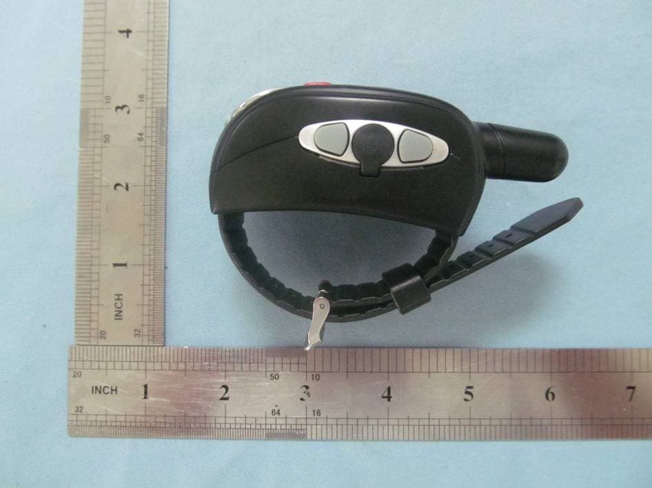
N3EWWWT70489
Nov 22, 2012Wrist Watch Walkie Talkie
Equipment Class
FRF - Part 95 Family Radio Face Held Transmitter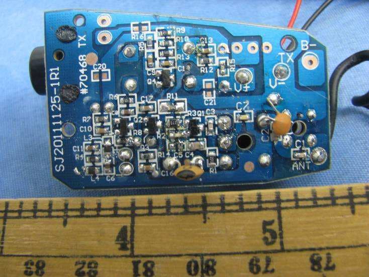
N3EUCLSR70468
May 06, 2012Spy Listener
Equipment Class
DXX - Part 15 Low Power Communication Device Transmitter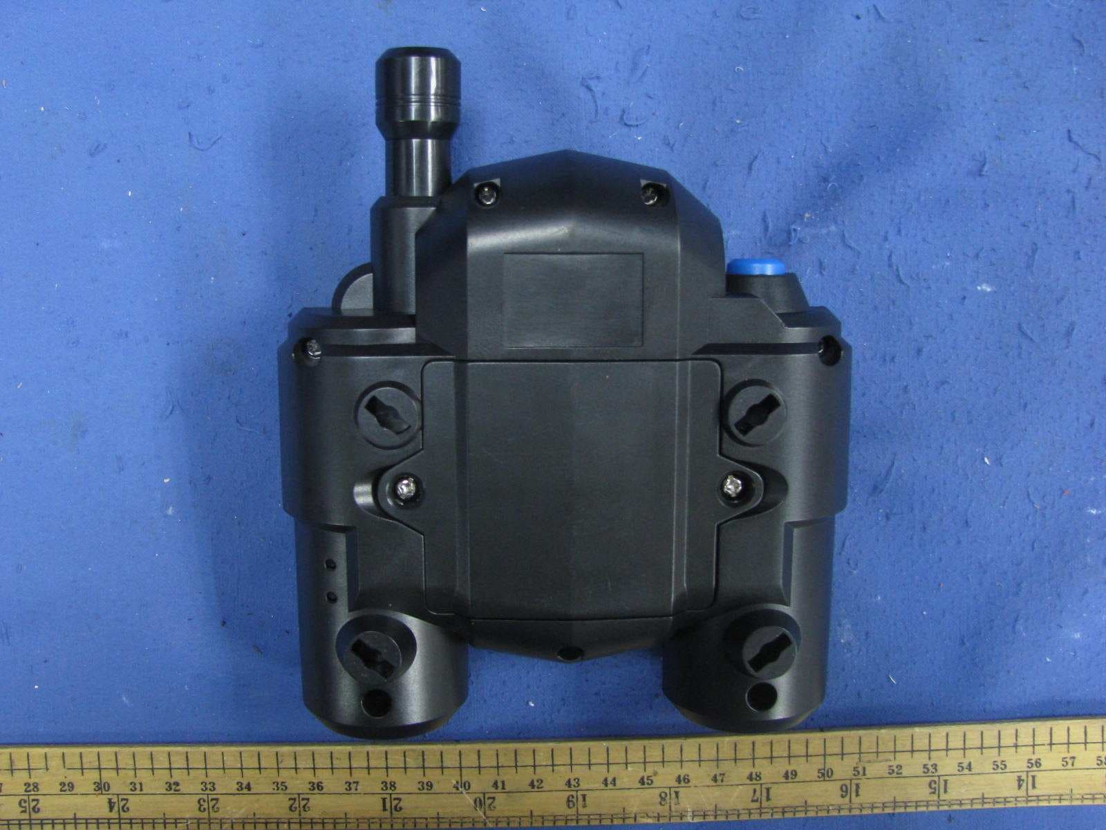
N3ESVC70436RX
Jun 07, 2011Spy Video Car
Equipment Class
DXX - Part 15 Low Power Communication Device Transmitter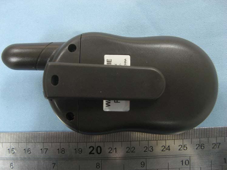
N3E74047
Apr 26, 2011long range walkie talkie; Model: 74047
Equipment Class
FRF - Part 95 Family Radio Face Held Transmitter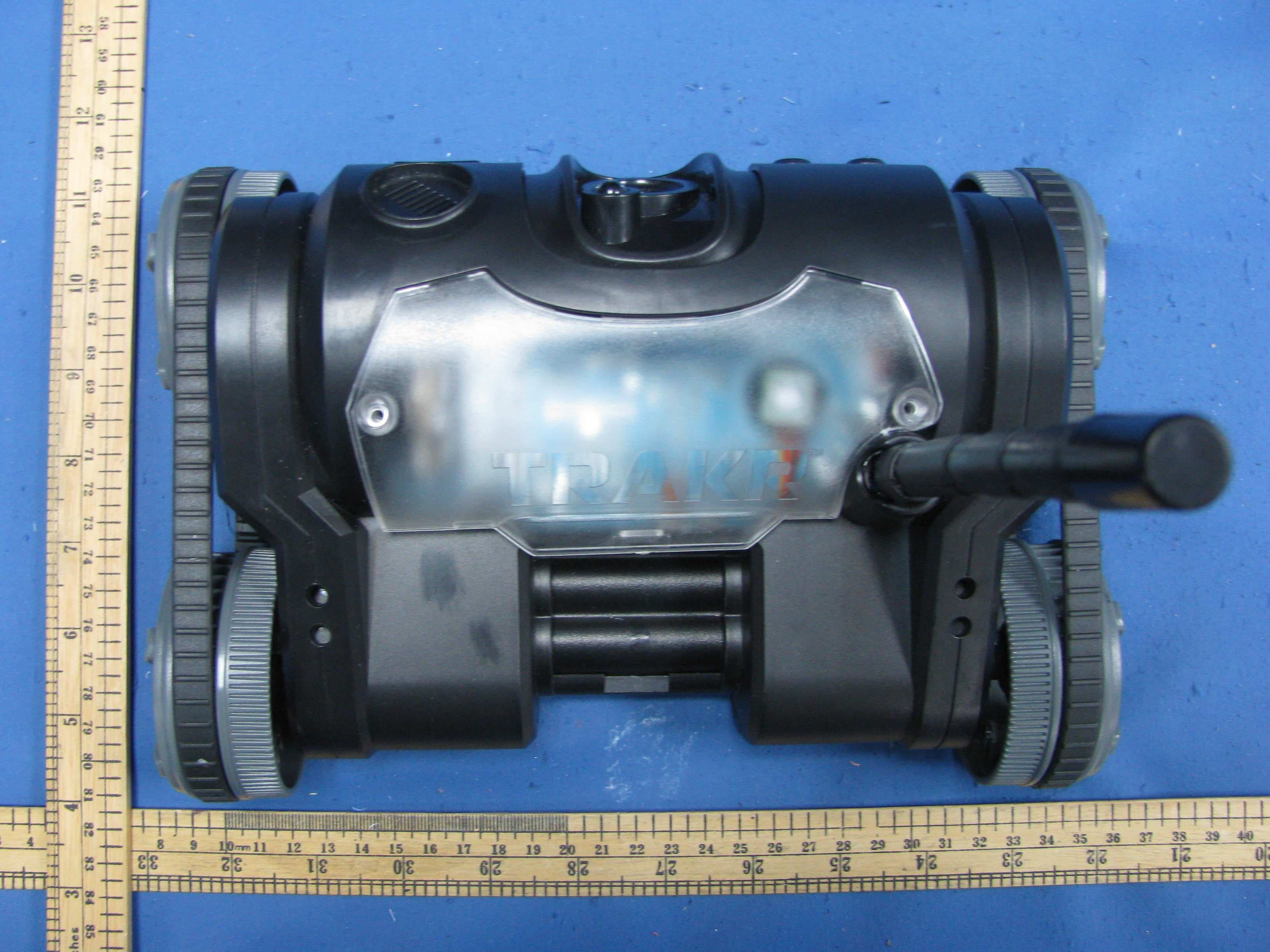
N3ESPYVIDEOTRAKR2
Jun 19, 2010Spy Video TRAKR
Equipment Class
JBP - Part 15 Class B Computing Device Peripheral