N8NLSD4WFWiFi Module
Lierda Science & Technology Group Co.,Ltd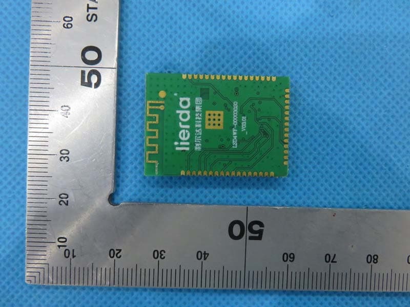
Click to zoom
Application Details
- Equipment Class
- DTS - Digital Transmission System
- Date of Grant
- Jul 09, 2015
- Application Purpose
- Original Equipment
- Date of Application
- Jul 09, 2015
- Equipment Note
- WiFi Module
- Frequency Range
- 2422.00000000 - 2452.00000000
- Country
- China
Documents & Files
Document Text
Text extracted from the exhibit documents filed with the FCC. Open a document above to read the original.
Users Manual
LierdaScience&TechnologyLtd LSDSCIENCE&TECHNOLOGYCO.,LTD. LSD4WF-2MD05101 LowPowerWi-FiModuleUserManual Model:LSD4WF-2MD05101 Name:Wi-FiModule Revision:v1.0 FCC ID:N8NLSD4WF Index 1.Productoverview.................................................................................................................................................3 1.1GeneralDescription..................................................................................................................................3 1.2Features........................................................................................................................................................3 2.Parameters.............................................................................................................................................................4 3.Package..................................................................................................................................................................4 4.Pindefinition.........................................................................................................................................................5 5.Behaviorofelectricity.........................................................................................................................................6 6.Typicalapplication...............................................................................................................................................7 7.Referencedesign.................................................................................................................................................7 8.Developingtool...................................................................................................................................................8 1.Productoverview 1.1GeneralDescription LSD4WF-2MD05101isaWi-Fimoduleforanyelectronicdevicetoachievenetworking capabilities.Themoduleisfullyinlinewiththe802.11b/g/ninternationalstandardspecification,the internalintegratedhighperformanceCortexM4andWi-Fichipmakeiteasytoaccesstheserialport equipmentorMCUcontrolequipmenttonetwork,soastorealizewirelessnetworking. Built-inTCP/IPprotocolstack,supportsSTA/AP/STA+APcoexistenceworkingmodes,supports 802.11b/g/nprotocol,supportswirelesslocalupgradeandOTAremotefirmwareupgrade. 32.8mmx23.1mmx3.2mm,usingthestampholepackage,built-inboardPCBantenna. 1.2Features Confirmwith802.11b/g/nprotocol. Built-inhighperformanceM4coreMCU,highestfrequency100MHz,highspeeddata processingability. USART/GPIO/SPI/PWMmultipleinterface. QJoinehighspeedlinkconfiguration. SupportSTA/AP/STA+APcoexistworkmode. SupportWPA/WPA2/WEPencryption. Supportwireless,WebpageandOTAremotehardwareupgrading. Supportmultiplenetprotocolcommunication. ProvideabundantAT+instructionsetconfiguration. Optionalbuilt-inonboardPCBantennaandexternalantennainterface. Dimension:32.8mmx23.1mmx3.2mm,Stampholepaste. 3.3Vsinglepowersupply. CE/FCC. RoHS. 2.Parameters Parameters Wireless Parameters Standard802.11b/g/n Frequency2.412GHz-2.462GHz Emittingpower Receiving Sensitivity 802.11b:-83dBm(@1Mbps,CCK) 802.11g:-74dBm(@54Mbps,OFDM) 802.11n:-61dBm(@HT20,MCS7) AntennaBuilt-in:OnboardPCBantenna Hardware Parameters WorkingVoltage 3.3V(3.0V~3.6V) WorkingCurrent QuiescentCurrent:~20mA EmittingpeakCurrent:~200mA Working Temperature -40°C~85°C Hardware Interface USART/GPIO/SPI/PWM Dimension32.8mmx23.1mmx3.2mm Software parameters Wirelessnetwork type STA/AP/STA+AP Security Mechanism WEP/WPA-PSK/WPA2-PSK EncryptionWEP/AES/TKIP Hardware upgrading Localwirelessupgrading/Webpage upgrading/Remoteupgrading NetworkProtocolIPv4,TCP/UDP/FTP/HTTP User Configuration QJoineConfiguration,AT+instruction,Web page Pic1-1LSD4WF-2MD05101BasicParameters 3.Package Pic1-2LSD4WF-2MD05101Frontandback 802.11b:+9.82dBm(@11Mbps) 802.11g:+8.27dBm(@54Mbps) 802.11n:+8.12dBm(@HT20,MCS7) Unit:mm Pic1-3LSD4WF-2MD05101modulepackagedimension 4.Pindefinition Pic1-4LSD4WF-2MD05101Modulepinlayout PinPindefinitionFunction 1GNDGroundpin 2SWCLKProgramdownloadport 5SWDIOProgramdownloadport 9VCCPowersupplypin(DC_3.3V) 17GNDGroundpin 20GPIO3/USART_CK/TIM1_CH1 Multiplexpin: IOport/USART/Timer 25WKUPModulewakeup 27GPIO1/USART_CTS/TIM1_CH4/SPI4_MISO Multiplexedpin: IOport/USART/timer/SPIport 28GPIO9/SPI4_SCK/TIM1_CH1N Multiplexpin: IOport/SPIport/timer 29GPIO8/SPI4_NSS/TIM1_BKIN Multiplexpin: IOport/SPIport/timer 30GPI07/ADC1_1/TIM2_CH2&TIME5_CH5/SPI4_MOSI Multiplexpin: IOport/ADC/timer/SPIport 31VCCPowersupplypin(DC_3.3V) 32GNDGroundpin 34VCC Powersupplypin(DC_3.3V) 39USART_TXUSARTportDatasendngport 40GPIO2/USART_RTS/TIM1_ETR Multiplexpin: IOport/USARTport/timer 41USART_RXUSARTportdatareceiver 42GPIO1/USART_CTS/TIM1_CH4/SPI4_MISO Multiplexpin: IOport/USARTport/timer/SPIport 43GPI04/ADC1_9/TIM3_CH4/nLinkMultiplexpin:IOport/ADC/timer 44GPI05/ADC1_8/TIM3_CH3/nReady Multiplexpin:IOport/ADC/timer 45GPI06/ADC1_4/nReloadMultiplexpin:IOport/ADC 47RST/nResetResetpin 48GNDGroundpin Table1-1LSD4WF-2MD05101Modulepindefinition 5.Behaviorofelectricity ParametersMinimumTypicalvalueMaximumUnit Workingvoltage3.03.33.6V Standbycurrent5mA Staticcurrent20mA TXcurrent200mA RXcurrent50mA Table1-2LSD4WF-2MD05101behaviorofelectricity 6.Typicalapplication Pic1-5LSD4WF-2MD05101Typicalcircuitconnection PinStateRemark NRST411Input,validinlowlevelModuleresetpinwithinternalpullresistor nlinkOutput(connectedtoLED)Checkthenetworkstateofmoduleorindication forbatchupgradeorconfiguration nReloadInput,validinlowlevelConnectbuttontochippinforfactorysetting restoring Sleep_RQInput,standbycontrolConnectbuttontochippinformoduledormancy managing Sleep_ONOutput,standbystateindicationIndicationofdormancystate,connectedwith LED USART_TX/USAR T_RX SerialporttransceiverportSerialporttransceiverport Table1-3Connectionintroductionofcardinalpin 7.Referencedesign PCBonboardantennaisbuiltinLSD4WF-2MD05101module,usersshouldusingonboardantenna designneedtobecautiousthat: 1,NocomponentsorGNDon…
Text truncated - open the document above for the full version.
Users Manual
LierdaScience&TechnologyLtd LSDSCIENCE&TECHNOLOGYCO.,LTD. LSD4WF-2MD05101 LowPowerWi-FiModuleUserManual Model:LSD4WF-2MD05101 Name:Wi-FiModule Revision:v1.0 FCC ID:N8NLSD4WF Index 1.Productoverview.................................................................................................................................................3 1.1GeneralDescription..................................................................................................................................3 1.2Features........................................................................................................................................................3 2.Parameters.............................................................................................................................................................4 3.Package..................................................................................................................................................................4 4.Pindefinition.........................................................................................................................................................5 5.Behaviorofelectricity.........................................................................................................................................6 6.Typicalapplication...............................................................................................................................................7 7.Referencedesign.................................................................................................................................................7 8.Developingtool...................................................................................................................................................8 1.Productoverview 1.1GeneralDescription LSD4WF-2MD05101isaWi-Fimoduleforanyelectronicdevicetoachievenetworking capabilities.Themoduleisfullyinlinewiththe802.11b/g/ninternationalstandardspecification,the internalintegratedhighperformanceCortexM4andWi-Fichipmakeiteasytoaccesstheserialport equipmentorMCUcontrolequipmenttonetwork,soastorealizewirelessnetworking. Built-inTCP/IPprotocolstack,supportsSTA/AP/STA+APcoexistenceworkingmodes,supports 802.11b/g/nprotocol,supportswirelesslocalupgradeandOTAremotefirmwareupgrade. 32.8mmx23.1mmx3.2mm,usingthestampholepackage,built-inboardPCBantenna. 1.2Features Confirmwith802.11b/g/nprotocol. Built-inhighperformanceM4coreMCU,highestfrequency100MHz,highspeeddata processingability. USART/GPIO/SPI/PWMmultipleinterface. QJoinehighspeedlinkconfiguration. SupportSTA/AP/STA+APcoexistworkmode. SupportWPA/WPA2/WEPencryption. Supportwireless,WebpageandOTAremotehardwareupgrading. Supportmultiplenetprotocolcommunication. ProvideabundantAT+instructionsetconfiguration. Optionalbuilt-inonboardPCBantennaandexternalantennainterface. Dimension:32.8mmx23.1mmx3.2mm,Stampholepaste. 3.3Vsinglepowersupply. CE/FCC. RoHS. 2.Parameters Parameters Wireless Parameters Standard802.11b/g/n Frequency2.412GHz-2.462GHz Emittingpower Receiving Sensitivity 802.11b:-83dBm(@1Mbps,CCK) 802.11g:-74dBm(@54Mbps,OFDM) 802.11n:-61dBm(@HT20,MCS7) AntennaBuilt-in:OnboardPCBantenna Hardware Parameters WorkingVoltage 3.3V(3.0V~3.6V) WorkingCurrent QuiescentCurrent:~20mA EmittingpeakCurrent:~200mA Working Temperature -40°C~85°C Hardware Interface USART/GPIO/SPI/PWM Dimension32.8mmx23.1mmx3.2mm Software parameters Wirelessnetwork type STA/AP/STA+AP Security Mechanism WEP/WPA-PSK/WPA2-PSK EncryptionWEP/AES/TKIP Hardware upgrading Localwirelessupgrading/Webpage upgrading/Remoteupgrading NetworkProtocolIPv4,TCP/UDP/FTP/HTTP User Configuration QJoineConfiguration,AT+instruction,Web page Pic1-1LSD4WF-2MD05101BasicParameters 3.Package Pic1-2LSD4WF-2MD05101Frontandback 802.11b:+9.82dBm(@11Mbps) 802.11g:+8.27dBm(@54Mbps) 802.11n:+8.12dBm(@HT20,MCS7) Unit:mm Pic1-3LSD4WF-2MD05101modulepackagedimension 4.Pindefinition Pic1-4LSD4WF-2MD05101Modulepinlayout PinPindefinitionFunction 1GNDGroundpin 2SWCLKProgramdownloadport 5SWDIOProgramdownloadport 9VCCPowersupplypin(DC_3.3V) 17GNDGroundpin 20GPIO3/USART_CK/TIM1_CH1 Multiplexpin: IOport/USART/Timer 25WKUPModulewakeup 27GPIO1/USART_CTS/TIM1_CH4/SPI4_MISO Multiplexedpin: IOport/USART/timer/SPIport 28GPIO9/SPI4_SCK/TIM1_CH1N Multiplexpin: IOport/SPIport/timer 29GPIO8/SPI4_NSS/TIM1_BKIN Multiplexpin: IOport/SPIport/timer 30GPI07/ADC1_1/TIM2_CH2&TIME5_CH5/SPI4_MOSI Multiplexpin: IOport/ADC/timer/SPIport 31VCCPowersupplypin(DC_3.3V) 32GNDGroundpin 34VCC Powersupplypin(DC_3.3V) 39USART_TXUSARTportDatasendngport 40GPIO2/USART_RTS/TIM1_ETR Multiplexpin: IOport/USARTport/timer 41USART_RXUSARTportdatareceiver 42GPIO1/USART_CTS/TIM1_CH4/SPI4_MISO Multiplexpin: IOport/USARTport/timer/SPIport 43GPI04/ADC1_9/TIM3_CH4/nLinkMultiplexpin:IOport/ADC/timer 44GPI05/ADC1_8/TIM3_CH3/nReady Multiplexpin:IOport/ADC/timer 45GPI06/ADC1_4/nReloadMultiplexpin:IOport/ADC 47RST/nResetResetpin 48GNDGroundpin Table1-1LSD4WF-2MD05101Modulepindefinition 5.Behaviorofelectricity ParametersMinimumTypicalvalueMaximumUnit Workingvoltage3.03.33.6V Standbycurrent5mA Staticcurrent20mA TXcurrent200mA RXcurrent50mA Table1-2LSD4WF-2MD05101behaviorofelectricity 6.Typicalapplication Pic1-5LSD4WF-2MD05101Typicalcircuitconnection PinStateRemark NRST411Input,validinlowlevelModuleresetpinwithinternalpullresistor nlinkOutput(connectedtoLED)Checkthenetworkstateofmoduleorindication forbatchupgradeorconfiguration nReloadInput,validinlowlevelConnectbuttontochippinforfactorysetting restoring Sleep_RQInput,standbycontrolConnectbuttontochippinformoduledormancy managing Sleep_ONOutput,standbystateindicationIndicationofdormancystate,connectedwith LED USART_TX/USAR T_RX SerialporttransceiverportSerialporttransceiverport Table1-3Connectionintroductionofcardinalpin 7.Referencedesign PCBonboardantennaisbuiltinLSD4WF-2MD05101module,usersshouldusingonboardantenna designneedtobecautiousthat: 1,NocomponentsorGNDon…
Text truncated - open the document above for the full version.
Cover Letter(s)
Date (06/07/2015) TUV SUD BABT TCB Octagon House, Segensworth Road, Fareham, Hampshire, PO15 5RL Confidentiality Request FCC ID: N8NLSD4WF Pursuant to Sections 0.457(d)(1)(ii) and 0.459 of the Commission’s Rules, Lierda Science & Technology Group Co.,Ltd hereby requests permanent confidential treatment of information accompanying this application as outlined below: 1.Schematics 2.Bill of Materials/Parts List 3.Block Diagrams 4.Theory of Operation The above materials contain trade secrets and proprietary information not customarily released to the public. The public disclosure of these matters might be harmful to the Applicant and provide unjustified benefits to its competitors. The Applicant understands that pursuant to Rule 0.457(d)(1)(ii), disclosure of this Application and all accompanying materials will not be made before the date of the Grant for this Application. Yours sincerely, Company Officer: Jimmy He Telephone Number: 0571-89908723 Email: [email protected]
Cover Letter(s)
Applicant Lierda Science & Technology Group Co.,Ltd FCC ID: N8NLSD4WF Section 15.212 Modular Transmitters Request for Modular Approval Y Request for Limited Modular Approval Requirements EUT Conditions Comply (Y/N) Single Modular Approval Requirements 1 The radio elements of the modular transmitter must have their own shielding. The physical crystal and tuning capacitors may be located external to the shielded radio elements. Yes, this RF Module has own RF shielding, please refer to the external photo Y 2 The modular transmitter must have buffered modulation/data inputs (if such inputs are provided) to ensure that the module will comply with Part 15 requirements under conditions of excessive data rates or over-modulation. Please refer the Schematic, The modular transmitter have buffered modulation/data inputs Y 3 The modular transmitter must have its own power supply regulation. The modular has it’s own power supply regulation. Y 4 The modular transmitter must comply with the antenna and transmission system requirements of Sections 15.203, 15.204(b) and 15.204(c). The antenna must either be permanently attached or employ a “unique” antenna coupler (at all connections between the module and the antenna, including the cable). The “professional installation” provision of Section 15.203 is not applicable to modules but can apply to limited modular approvals under paragraph (b) of this section. Referring to onboard PCB antenna Y 5 The modular transmitter must be tested in a stand-alone configuration, i.e., the module must not be inside another device during testing for compliance with Part 15 requirements. Unless the transmitter module will be battery powered, it must comply with the AC line conducted requirements found in Section 15.207. AC or DC power lines and data input/output lines connected to the module must not contain ferrites, unless they will be marketed with the module (see Section 15.27(a)). The length of these lines shall be the length typical of actual use or, if that length is unknown, at least 10 centimeters to insure that there is no coupling between the case of the module and supporting equipment. Any accessories, peripherals, or support equipment connected to the module during testing shall be unmodified and commercially available equipment. Any accessories, peripherals, or support equipment connected to the module during testing shall be unmodified and commercially available (see Section 15.31(i)). Referring to the test setup photos. This module is tested in a stand-alone configuration. Y 6 The modular transmitter must be equipped with either a permanently affixed label or must be capable of electronically displaying its FCC identification number. (A) If using a permanently affixed label, the modular transmitter must be labeled with its own FCC identification number, and, if the FCC identification number is not visible when the module is installed inside another device, then the outside of the device into which the module is installed must also display a label referring to the enclosed module. This exterior label can use wording such as the following: “Contains Transmitter Module FCC ID: XYZMODEL1” or “Contains FCC ID: XYZMODEL1.” Any similar wording that expresses the same meaning may be used. The Grantee may either provide such a label, an example of which must The modular was labeled with its own FCC ID. The outside of device in to which the module is installed will labeled ‘Contains TX FCC ID: N8NLSD4WF, Please refer to User Manual Y be included in the application for equipment authorization, or, must provide adequate instructions along with the module which explain this requirement. In the latter case, a copy of these instructions must be included in the application for equipment authorization. (B) If the modular transmitter uses an electronic display of the FCC identification number, the information must be readily accessible and visible on the modular transmitter or on the device in which it is installed. If the module is installed inside another device, then the outside of the device into which the module is installed must display a label referring to the enclosed module. This exterior label can use wording such as the following: “Contains FCC certified transmitter module(s).” Any similar wording that expresses the same meaning may be used. The user manual must include instructions on how to access the electronic display. A copy of these instructions must be included in the application for equipment authorization. 7 The modular transmitter must comply with any specific rules or operating requirements that ordinarily apply to a complete transmitter and the manufacturer must provide adequate instructions along with the module to explain any such requirements. A copy of these instructions must be included in the application for equipment authorization. The modular is comply with all applicable FCC rules. Any modifications, not expressly approved by the manufacturer could void the authority to operate in these regions. Y 8 The modular transmitter must comply with any applicable RF exposure requirements in its final configuration. With the documented max output power this RF Module meets the FCC SAR Exemption - so it can be integrated in any host device (portable/mobile/fixed) with further restrictions. Y A limited modular approval may be granted for single or split modular transmitters that do not comply with all of the above requirements, e.g., shielding, minimum signaling amplitude, buffered modulation/data inputs, or power supply regulation, if the manufacturer can demonstrate by alternative means in the application for equipment authorization that the modular transmitter meets all the applicable Part 15 requirements under the operating conditions in which the transmitter will be used. Limited modular approval also may be granted in those instances where compliance with RF exposure rules is demonstrated only for particular product configurations. The applicant for …
Text truncated - open the document above for the full version.
Cover Letter(s)
Date (06/07/2015) TUV SUD BABT TCB Octagon House, Segensworth Road, Fareham, Hampshire, PO15 5RL Confidentiality Request FCC ID: N8NLSD4WF Pursuant to Sections 0.457(d)(1)(ii) and 0.459 of the Commission’s Rules, Lierda Science & Technology Group Co.,Ltd hereby requests permanent confidential treatment of information accompanying this application as outlined below: 1.Schematics 2.Bill of Materials/Parts List 3.Block Diagrams 4.Theory of Operation The above materials contain trade secrets and proprietary information not customarily released to the public. The public disclosure of these matters might be harmful to the Applicant and provide unjustified benefits to its competitors. The Applicant understands that pursuant to Rule 0.457(d)(1)(ii), disclosure of this Application and all accompanying materials will not be made before the date of the Grant for this Application. Yours sincerely, Company Officer: Jimmy He Telephone Number: 0571-89908723 Email: [email protected]
Cover Letter(s)
Applicant Lierda Science & Technology Group Co.,Ltd FCC ID: N8NLSD4WF Section 15.212 Modular Transmitters Request for Modular Approval Y Request for Limited Modular Approval Requirements EUT Conditions Comply (Y/N) Single Modular Approval Requirements 1 The radio elements of the modular transmitter must have their own shielding. The physical crystal and tuning capacitors may be located external to the shielded radio elements. Yes, this RF Module has own RF shielding, please refer to the external photo Y 2 The modular transmitter must have buffered modulation/data inputs (if such inputs are provided) to ensure that the module will comply with Part 15 requirements under conditions of excessive data rates or over-modulation. Please refer the Schematic, The modular transmitter have buffered modulation/data inputs Y 3 The modular transmitter must have its own power supply regulation. The modular has it’s own power supply regulation. Y 4 The modular transmitter must comply with the antenna and transmission system requirements of Sections 15.203, 15.204(b) and 15.204(c). The antenna must either be permanently attached or employ a “unique” antenna coupler (at all connections between the module and the antenna, including the cable). The “professional installation” provision of Section 15.203 is not applicable to modules but can apply to limited modular approvals under paragraph (b) of this section. Referring to onboard PCB antenna Y 5 The modular transmitter must be tested in a stand-alone configuration, i.e., the module must not be inside another device during testing for compliance with Part 15 requirements. Unless the transmitter module will be battery powered, it must comply with the AC line conducted requirements found in Section 15.207. AC or DC power lines and data input/output lines connected to the module must not contain ferrites, unless they will be marketed with the module (see Section 15.27(a)). The length of these lines shall be the length typical of actual use or, if that length is unknown, at least 10 centimeters to insure that there is no coupling between the case of the module and supporting equipment. Any accessories, peripherals, or support equipment connected to the module during testing shall be unmodified and commercially available equipment. Any accessories, peripherals, or support equipment connected to the module during testing shall be unmodified and commercially available (see Section 15.31(i)). Referring to the test setup photos. This module is tested in a stand-alone configuration. Y 6 The modular transmitter must be equipped with either a permanently affixed label or must be capable of electronically displaying its FCC identification number. (A) If using a permanently affixed label, the modular transmitter must be labeled with its own FCC identification number, and, if the FCC identification number is not visible when the module is installed inside another device, then the outside of the device into which the module is installed must also display a label referring to the enclosed module. This exterior label can use wording such as the following: “Contains Transmitter Module FCC ID: XYZMODEL1” or “Contains FCC ID: XYZMODEL1.” Any similar wording that expresses the same meaning may be used. The Grantee may either provide such a label, an example of which must The modular was labeled with its own FCC ID. The outside of device in to which the module is installed will labeled ‘Contains TX FCC ID: N8NLSD4WF, Please refer to User Manual Y be included in the application for equipment authorization, or, must provide adequate instructions along with the module which explain this requirement. In the latter case, a copy of these instructions must be included in the application for equipment authorization. (B) If the modular transmitter uses an electronic display of the FCC identification number, the information must be readily accessible and visible on the modular transmitter or on the device in which it is installed. If the module is installed inside another device, then the outside of the device into which the module is installed must display a label referring to the enclosed module. This exterior label can use wording such as the following: “Contains FCC certified transmitter module(s).” Any similar wording that expresses the same meaning may be used. The user manual must include instructions on how to access the electronic display. A copy of these instructions must be included in the application for equipment authorization. 7 The modular transmitter must comply with any specific rules or operating requirements that ordinarily apply to a complete transmitter and the manufacturer must provide adequate instructions along with the module to explain any such requirements. A copy of these instructions must be included in the application for equipment authorization. The modular is comply with all applicable FCC rules. Any modifications, not expressly approved by the manufacturer could void the authority to operate in these regions. Y 8 The modular transmitter must comply with any applicable RF exposure requirements in its final configuration. With the documented max output power this RF Module meets the FCC SAR Exemption - so it can be integrated in any host device (portable/mobile/fixed) with further restrictions. Y A limited modular approval may be granted for single or split modular transmitters that do not comply with all of the above requirements, e.g., shielding, minimum signaling amplitude, buffered modulation/data inputs, or power supply regulation, if the manufacturer can demonstrate by alternative means in the application for equipment authorization that the modular transmitter meets all the applicable Part 15 requirements under the operating conditions in which the transmitter will be used. Limited modular approval also may be granted in those instances where compliance with RF exposure rules is demonstrated only for particular product configurations. The applicant for …
Text truncated - open the document above for the full version.
External Photos
External Photos TOP VIEW OF EUT BOTTOM VIEW OF EUT Antenna
ID Label/Location Info
FCC ID Label Location FCC ID: N8NLSD4WF Model: LSD4WF-2MD05101 FCC ID:N8NLSD4WF
Internal Photos
Internal Photos INTERNAL VIEW OF EUT
Internal Photos
Internal Photos INTERNAL VIEW OF EUT
RF Exposure Info
RF Exposure (FCC ID: N8NLSD4WF) Applicable Standard According to §1.1307(b)(5), systems operating under the provisions of this section shall be operated in a manner that ensure that the public is not exposed to radio frequency energy level in excess of the Commission’s guideline. This is a Portable device. KDB447498 D01 V05 was used as the guidance. Maximum measured transmitter Conducted Power: 802.11b Maximum Conducted Power (AV) (dBm) Maximum Conducted Power (mW) 9.82 9.59 Maximum measured transmitter Conducted Power: 802.11g Maximum Conducted Power (AV) (dBm) Maximum Conducted Power (mW) 8.27 6.71 Maximum measured transmitter Conducted Power: 802.11n HT20 Maximum Conducted Power (AV) (dBm) Maximum Conducted Power (mW) 8.12 6.49 Maximum measured transmitter Conducted Power: 802.11n HT40 Maximum Conducted Power (AV) (dBm) Maximum Conducted Power (mW) 6.31 4.28 Refer to 447498 25 D01 General RF Exposure Guidance v05 Appendix A, you see that for Maximum Conducted Output Power 9.59mW (<10mW), so no SAR is required.
RF Exposure Info
RF Exposure (FCC ID: N8NLSD4WF) Applicable Standard According to §1.1307(b)(5), systems operating under the provisions of this section shall be operated in a manner that ensure that the public is not exposed to radio frequency energy level in excess of the Commission’s guideline. This is a Portable device. KDB447498 D01 V05 was used as the guidance. Maximum measured transmitter Conducted Power: 802.11b Maximum Conducted Power (AV) (dBm) Maximum Conducted Power (mW) 9.82 9.59 Maximum measured transmitter Conducted Power: 802.11g Maximum Conducted Power (AV) (dBm) Maximum Conducted Power (mW) 8.27 6.71 Maximum measured transmitter Conducted Power: 802.11n HT20 Maximum Conducted Power (AV) (dBm) Maximum Conducted Power (mW) 8.12 6.49 Maximum measured transmitter Conducted Power: 802.11n HT40 Maximum Conducted Power (AV) (dBm) Maximum Conducted Power (mW) 6.31 4.28 Refer to 447498 25 D01 General RF Exposure Guidance v05 Appendix A, you see that for Maximum Conducted Output Power 9.59mW (<10mW), so no SAR is required.
Test Report
Page 1 of 88 Report No.: AGC01162150501FE04 FCC ID : N8NLSD4WF APPLICATION PURPOSE : Original Equipment PRODUCT DESIGNATION : Wi‐Fi Module BRAND NAME : N/A MODEL NAME : LSD4WF‐2MD05101 CLIENT : Lierda Science & Technology Group Co., Ltd. DATE OF ISSUE : Jun.19, 2015 STANDARD(S) TEST PROCEDURE(S) : FCC Part 15.247 KDB 558074 v03r02 REPORT VERSION : V1.0 Attestation of Global Compliance (Shenzhen) Co., Ltd CAUTION: This report shall not be reproduced except in full without the written permission of the test laboratory and shall not be quoted out of context. FCC Test Report Report No.: AGC01162150501FE04 Page 2 of 88 Report Revise Record Report Version Revise Time Issued Date Valid VersionNotes V1.0 / Jun.19, 2015Valid Original Report Report No.: AGC01162150501FE04 Page 3 of 88 TABLE OF CONTENTS 1. VERIFICATION OF CONFORMITY ............................................................................................................ 5 2. GENERAL INFORMATION ........................................................................................................................ 6 2.1. PRODUCT DESCRIPTION ................................................................................................................. 6 2.2. TABLE OF CARRIER FREQUENCYS ................................................................................................ 6 2.3. IEEE 802.11N MODULATION SCHEME ............................................................................................. 7 2.4. RELATED SUBMITTAL(S) / GRANT (S) ............................................................................................. 7 2.5. TEST METHODOLOGY .....................................................................................................................…
Text truncated - open the document above for the full version.
Contact Information
Applicant
Qingqing Sun(Certified Engineer)
Test Firm
Compliance Certification Services (Shenzhen) Inc.Harry Li
Technical Specifications
| # | Rule Parts | Frequency Range | Power Output |
|---|---|---|---|
| 2 | 15C | 2.42 GHz - 2.45 GHz | 4.30 mW |
Other Applications from Lierda Science & Technology Group Co.,Ltd
N8NLSD4BT-T55
Aug 24, 2021Bluetooth Module
Equipment Class
DTS - Digital Transmission System
N8NLSD4RF043610D0
Mar 03, 20212.4GHz Wireless Module
Equipment Class
DXX - Part 15 Low Power Communication Device Transmitter
N8NLSD4BT-S95
Jul 02, 2020S95 module
Equipment Class
DTS - Digital Transmission System
N8NLSD4BTP74MSTD1
Feb 15, 2015P-series BLE Module
Equipment Class
DTS - Digital Transmission System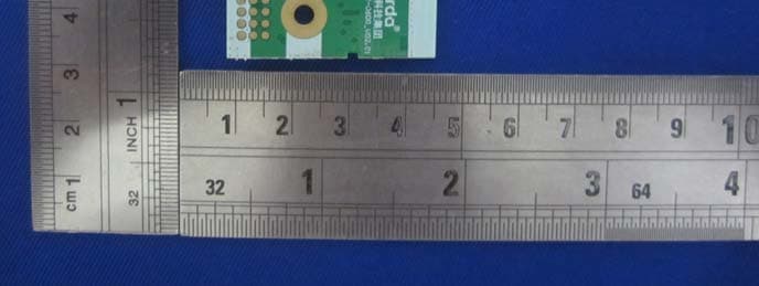
N8NLSD4BT212-06D0
Jun 08, 2014Bluetooth Module
Equipment Class
DTS - Digital Transmission System