NDX-OMNIMAX2RFID Scanner with Bluetooth Low Energy
Datamars SAApplication Details
- Equipment Class
- DCD - Part 15 Low Power Transmitter Below 1705 kHz
- Date of Grant
- Jun 02, 2026
- Application Purpose
- Original Equipment
- Equipment Note
- RFID Scanner with Bluetooth Low Energy
- Frequency Range
- 0.13400000 - 0.13400000
- Company
- Datamars SA
- Country
- Switzerland
Documents & Files
Document Text
Text extracted from the exhibit documents filed with the FCC. Open a document above to read the original.
Attestation Statements
1|1 DR003886 FCC Certifications concerning “covered” equipment (as required by section 2.911(d)(5)(i)-(ii)) – OmniMax+ – NDX-OMNIMAX2 Date: 30/03/2026 Federal Communications Commission Equipment Authorization Branch 7435 Oakland Mills Rd. Columbia MD 21046 FCC ID: NDX-OMNIMAX2 We, Datamars SA, Via Industria 16, 6814 Lamone, Switzerland, hereby certify that: • the equipment for which authorization is sought is not “covered” equipment prohibited from receiving an equipment authorization pursuant to section 2.903 of the FCC rules. • as of the date of the filing of the application, the applicant is not identified on the Covered List as an entity producing “covered” equipment. Also, we certify that the equipment for which authorization is sought does not contain or includes equipment with integrated cybersecurity and anti-virus software produced or provided by Kaspersky Lab, Inc. or any of its successors and assignees. Sincerely, __________________________ By: Damien Pachoud Title: Chief Production and Technology Officer Company: Datamars SA Telephone: +41 91 935 73 40 e-mail: [email protected]
Cover Letter(s)
1|1 DR003887 FCC Agent letter – OmniMax+ – NDX-OMNIMAX2 Date: 30/03/2026 Federal Communications Commission Equipment Authorization Branch 7435 Oakland Mills Rd. Columbia MD 21046 FCC ID: NDX-OMNIMAX2 We, Datamars SA, Via Industria 16, 6814 Lamone, Switzerland, hereby authorize, DEKRA Testing and Certification S.A.U. Parque Tecnológico de Andalucía C/Severo Ochoa, 2 & 6 | 29590 | Málaga | Spain Agent: Álvaro Corrales Sedeño e-mail: [email protected] Phone: +34 952 619 198 to act as our agent in the preparation of this application for equipment certification, including the signing of all documents relating to these matters. We also hereby certify that neither we nor any party to this application are subject to a denial of U.S. Federal benefits, which include FCC benefits, pursuant to Section 5301 of the Anti-Drug Abuse Act of 1988, U.S.C. 862 because of conviction for possession or distribution of controlled substance. For instances where our authorized agent signs the application for certification on our behalf, I acknowledge that all responsibility for complying with the terms and conditions for Certification, as specified by DEKRA Testing and Certification, S.A.U., still resides with us. This agreement expires one year from the current date. Sincerely, __________________________ By: Damien Pachoud Title: Chief Production and Technology Officer Company: Datamars SA Telephone: +41 91 935 73 40 e-mail: [email protected]
Cover Letter(s)
1|2 DR003885 FCC Confidentiality request – OmniMax+ – NDX-OMNIMAX2 Date: 30/03/2026 Federal Communications Commission Equipment Authorization Branch 7435 Oakland Mills Rd. Columbia MD 21046 FCC ID: NDX-OMNIMAX2 We, Datamars SA, Via Industria 16, 6814 Lamone, Switzerland, hereby request requests that a part of the subject FCC application be held confidential to avoid release of sensitive information of the product to the public pursuant to §0.457(d)(1)(ii) and §0.459 of the Commission’s Rules (47 C.F.R.) and §552 (b)(4) of the Freedom of Information Act. For the product stated above, we request that the following information be withheld from public disclose: Type of Confidentiality Requested Exhibit Short Term Permanent Block Diagrams Short Term Permanent Operation Description Short Term Permanent Schematics Short Term Permanent Parts List & Placement/BOM Short Term Permanent Tune-Up Procedure Short Term Permanent SDR Software and Security Information Short Term Test Setup Photos Short Term User’s Manual Short Term External Photos Short Term Internal Photos Permanent Confidentiality: The above materials contain trade secrets and proprietary information not customarily released to the public. The public disclosure of these matters might be harmful to us and provide unjustified benefits to our competitors. Short-Term Confidentiality: We hereby request short-term confidentiality for the product stated above to avoid premature release of sensitive information prior to marketing or release of the product to the public. Release date of short-term confidentiality is: 45 days from grant date marked 90 days from grant date marked 135 days from grant date marked 180 days from grant date marked Specific date: 2|2 DR003885 We are also aware that we are responsible to notify DEKRA Testing and Certification S.A.U. in the event information regarding the product or the product is made available to the public. DEKRA Testing and Certification S.A.U. will then release the documents listed above for public disclosure pursuant to FCC Public Notice DA 04-1705. Sincerely, __________________________ By: Damien Pachoud Title: Chief Production and Technology Officer Company: Datamars SA Telephone: +41 91 935 73 40 e-mail: [email protected]
Cover Letter(s)
1|1 DR003884 FCC Supplier’s Declaration of Conformity (SDoC) – OmniMax+ – NDX-OMNIMAX2 Date: 30/03/2026 Federal Communications Commission Equipment Authorization Branch 7435 Oakland Mills Rd. Columbia MD 21046 FCC ID: NDX-OMNIMAX2 We, Datamars SA, Via Industria 16, 6814 Lamone, Switzerland, pursuant to §15.101 of the Commission’s Rules (47 C.F.R.), hereby declare that the device above mentioned is classified under the following equipment class/classes: JAB Part 15 Class B Digital Device JAD Part 15 Class A Digital Device JAV Other Non-Digital SDoC Devices JBP Part 15 Class B Computing Device Peripheral JBC Part 15 Class B Computing Device/Personal Computer CXX Communications Rcvr for use w/ licensed Tx and CBs CRR Superregenerative Receiver CYY Communications Receiver used w/Pt 15 Transmitter HID Part 15 TV Interface Device and we will follow the Supplier’s Declaration of Conformity authorization procedure prior to the initiation of marketing. Sincerely, __________________________ By: Damien Pachoud Title: Chief Production and Technology Officer Company: Datamars SA Telephone: +41 91 935 73 40 e-mail: [email protected]
RF Exposure Info
DEKRA Testing and Certification, S.A.U. Parque Tecnológico de Andalucía, c/ Severo Ochoa nº 2 · 29590 Campanillas · Málaga · España C.I.F. A29 507 456 Report No: (NIE) 84605RAN.003A1 2026-04-01 Test report No: NIE: 84605RAN.003A1 Assessment report RF EXPOSURE REPORT ACCORDING TO FCC 47 CFR Part 2.1093 FCC 47 CFR Part 1.1307 (*) Identification of item under evaluation OMNI MAX + (*) Trademark DATAMARS (*) Model and /or type reference OMNI MAX + (*) Other identification of the product FCC ID : NDX-OMNIMAX2 IC ID : 4678A-OMNIMAX2 HW version : 1V1 SW Version : 2.0.0 (*) Features BLE and RFID (*) Manufacturer DATAMARS SA via Industria 16, 6814 Lamone, Switzerland Test method requested, standard FCC 47 CFR Part 2.1093. Radiofrequency radiation exposure evaluation: portable devices. FCC 47 CFR Part 1.1307: Actions that may have a significant environmental effect, for which Environmental Assessments (EAs) must be prepared. Summary IN COMPLIANCE Approved by (name / position & signature) Manuel García Antennas Lab Technical Responsible Date of issue 2026-04-01 Report template No FAN24_03 (*) “Data provided by the client” DEKRA Testing and Certification, S.A.U. Parque Tecnológico de Andalucía, c/ Severo Ochoa nº 2 · 29590 Campanillas · Málaga · España C.I.F. A29 507 456 Report No: (NIE) 84605RAN.003A1 Page 2 of 11 2026-04-01 Index Competences and guarantees .................................................................................................... 3 General conditions ...................................................................................................................... 3 Data provided by the client .......................................................................................................... 3 Identification of the client............................................................................................................. 5 Document history ........................................................................................................................ 5 Appendix A: FCC RF Exposure assessment result ..................................................................... 6 General description of the device under evaluation ................................................................ 7 Evaluation Results .................................................................................................................. 7 Appendix B: FCC RF Exposure information ................................................................................ 9 RF Exposure determination of exemption ............................................................................. 10 DEKRA Testing and Certification, S.A.U. Parque Tecnológico de Andalucía, c/ Severo Ochoa nº 2 · 29590 Campanillas · Málaga · España C.I.F. A29 507 456 Report No: (NIE) 84605RAN.003A1 Page 3 of 11 2026-04-01 Competences and guarantees In order to assure the traceability to other national and international laboratories, DEKRA Testing and Certification, S.A.U. has a calibration and maintenance program for its measurement equipment. DEKRA Testing and Certification, S.A.U. guarantees the reliability of the data presented in this report, which is the result of the measurements and the tests performed to the item under test on the date and under the conditions stated on the report and, it is based on the knowledge and technical facilities available at DEKRA Testing and Certification, S.A.U. at the time of performance of the test. DEKRA Testing and Certification, S.A.U. is liable to the client for the maintenance of the confidentiality of all information related to the item under test and the results of the test. The results presented in this Assessment Report apply only to the particular item under test established in this document. IMPORTANT: No parts of this report may be reproduced or quoted out of context, in any form or by any means, except in full, without the previous written permission of DEKRA Testing and Certification, S.A.U. General conditions 1. This report is only referred to the item that has undergone the assessment. 2. This report does not constitute or imply on its own an approval of the product by the Certification Bodies or competent Authorities. 3. This document is only valid if complete; no partial reproduction can be made without previous written permission of DEKRA Testing and Certification, S.A.U. 4. This assessment report cannot be used partially or in full for publicity and/or promotional purposes without previous written permission of DEKRA Testing and Certification, S.A.U. Data provided by the client The following data has been provided by the client: 1. Information relating to the description of the sample ("Identification of the item under evaluation", "Trademark", "Model and/or type reference", “General description of the device”, “Other identification of the product”). 2. Maximum output power, maximum antenna gain and use distance information. 3. The device under evaluation consists of a Portable Bluetooth® Reader for Animal Identification. 4. Duty cycle and average exposure-time. DEKRA Testing and Certification, S.A.U. Parque Tecnológico de Andalucía, c/ Severo Ochoa nº 2 · 29590 Campanillas · Málaga · España C.I.F. A29 507 456 Report No: (NIE) 84605RAN.003A1 Page 4 of 11 2026-04-01 DEKRA Testing and Certification S.A.U. declines any responsibility with respect to the information provided by the client and that may affect the validity of results. DEKRA Testing and Certification, S.A.U. Parque Tecnológico de Andalucía, c/ Severo Ochoa nº 2 · 29590 Campanillas · Málaga · España C.I.F. A29 507 456 Report No: (NIE) 84605RAN.003A1 Page 5 of 11 2026-04-01 Identification of the client DATAMARS SA via Industria 16, 6814 Lamone, Switzerland Document history Report number Date Description 84605RAN.003 2026-02-23 First release 84605RAN.003A1 2026-04-01 Second release. Bluetooth maximum conducted output power has been updated. This test report cancels and replaces test report 84605…
Text truncated - open the document above for the full version.
Test Report
Introduction This application note is dedicated to the STM32WB and STM32WB0 series microcontrollers. One of the main reasons to use a printed circuit board (PCB) antenna is the reduced overall cost of the radio module. Well- designed and implemented PCB-printed antennae have a similar performance to the SMD (surface-mounted device) ceramic equivalence. In general, the footprint for a ceramic SMD antenna is smaller than that for a PCB-printed variant. For a PCB-printed antenna solution, the increased size of the PCB in relation to the space required for the antenna means that the radio module is larger, increasing the cost of the PCB. However, the PCB solution is generally cheaper than an SMD ceramic antenna. The demonstration and development boards for the STM32WB and STM32WB0 series implement PCB-printed antennae based on this application note. Guidelines for meander design using low-cost PCB antennae with 2.4 GHz radio for STM32WB/WB0 MCUs AN5129 Application note AN5129 - Rev 5 - April 2024 For further information contact your local STMicroelectronics sales office. www.st.com 1 General information This document applies to STM32WB and STM32WB0 series Arm ® based devices. Note:Arm is a registered trademark of Arm Limited (or its subsidiaries) in the US and/or elsewhere. AN5129 General information AN5129 - Rev 5 page 2/22 2 Coordinate system For the purpose of this document, the spherical coordinate system illustrated in the figure below is used. Figure 1. Spherical coordinate system The PCB module is orientated vertically (plane X-Z) and located in proximity to the origin of the coordinate system. The azimuth angle radiates from the X-axis towards the Y-axis and the elevation angle radiates from the Z-axis towards the horizontal X-Y plane. Sometimes, as with geographical and navigational systems, the X-axis is called the "Nord-axis", the Yaxis is called the "East-axis" and the Z-axis is called the "Zenith-axis". AN5129 Coordinate system AN5129 - Rev 5 page 3/22 3 Layout specification The PCB antennas, including the electrical parameters of PCB materials used, are layout sensitive. It is recommended to use a layout as close as possible to the one shown in the figure below. Figure 2. PCB antenna dimensions (in mm) The electrical parameters and performance of the PCB antenna are also determined by the substrate used, in particular the thickness of the core and dielectric constants. AN5129 Layout specification AN5129 - Rev 5 page 4/22 The figure below illustrates a typical cross-section of the substrate in a PCB-antennae area. Figure 3. PCB cross section at antennae area A substrate with the parameters as defined in the table below is recommended. Table 1. Recommended substrate specification Layer Dimensions Dielectric constant Ɛ R LabelValue (mil)Value (μm) Solder mask, top S10.717.78 4.4 Copper traceT1.640.64- CoreC28711.24.4 Solder mask, bottomS20.717.784.4 AN5129 Layout specification AN5129 - Rev 5 page 5/22 4 Impedance matching Meander-like PCB antennae can be tuned to the required 50‑Ω impedance by matching the impedance circuitry with the π topology. In Figure 2, the impedance matching area is marked with a dashed line. Under nominal conditions, this antenna exhibits and impedance very close to the required nominal impedance (50 Ω). To check the performance of this design, a sample antenna was manufactured (according to the specifications covered by this document). The figure below shows this antenna. Figure 4. Part of 802.15.4 and BLE PCB with meander-like antenna (scale approximately 4:1) Assuming that the manufactured sample exhibits the expected performance (no impedance matching necessary), the impedance matching circuitry is bypassed by two 100‑pF capacitors connected in series, as shown in the figure below. Figure 5. Bypassing impedance matching circuitry - Direct RF connection All electrical parameters of the meander-like antenna have been measured at connection to the band-pass filter (BPF) with the frequency span covering frequencies from 2.4 GHz to 2.5 GHz. AN5129 Impedance matching AN5129 - Rev 5 page 6/22 The figure below shows the complex impedance of the antenna in a Smith chart. Figure 6. Complex impedance of the meander-like antenna (Smith chart) The figure below shows the magnitude of the S11 parameter (in log scale). Figure 7. S11 parameter in logarithmic scale (Cartesian plot) AN5129 Impedance matching AN5129 - Rev 5 page 7/22 The figure below shows the standing wave ratio (SWR). Figure 8. Antenna standing wave ratio (SWR) The following changes affect the radiation impedance of the PCB antenna: •Board size variation •Metal shielding •Use of plastic cover •Presence of other components in proximity of the antenna The best performance impedance matching circuitry compensates these effects so that, for operating frequencies, the optimum 50‑Ω impedance is achieved. AN5129 Impedance matching AN5129 - Rev 5 page 8/22 5 Radiation pattern, 3-D visualization A three-dimensional (3-D) visualization of the radiation pattern (magnitude of the electrical far field |E|) is done for the center ISM band frequency 2.44175 GHz. Figure 9. 3-D radiation pattern overview Figure 10. Radiation pattern on X-Z plane AN5129 Radiation pattern, 3-D visualization AN5129 - Rev 5 page 9/22 6 Radiation pattern, 2-D visualization In this section, all radiation patterns are related to the magnitude of the electrical far field |E|, which is normalized and shown in the logarithmic scale (in dB). This means that the maximum global radiation pattern (maximum magnitude of the electrical far-field |E|) is represented by a 0 dB level. To show the antenna radiation patterns in detail, three two-dimensional (2-D) major cuts are presented. Consider the orientation of the module in the spherical coordinate system as shown in Figure 1. A three-dimensional (3-D) far field radiation pattern is visualized as three 2-D cuts through a 3-D pattern. The following major planes are used for these cuts (see Figure 11): •…
Text truncated - open the document above for the full version.
Test Report
ANTENNA DATA INFORMATION The OMNI MAX+ has 1 PCB antenna for the Bluetooth LE interface and 1 coil antenna (several loops of wire) for the 134 kHz inductive interface. The antenna for the Bluetooth interface is based on a reference design from STMicroelectronics for their chip STM32WB55 which is the chipset providing the Bluetooth functionality to our Product. The maximum antenna gain measured was -1.8 dBi. Please refer to the additional document to know more about the design. The antenna for the 134 kHz inductive interface is a coiled wire along the contour of the device as shown in the next drawing and picture. This loop plugs into the PCB inside. Antenna gain is not applicable in this case.
Test Report
1 (35) Copyright © Verkotan 2026 Document ID: FCC EMF Test Report_OMNI MAX +_ID7710_11022026.docx EMF Evaluation Report Date of Report: 23/02/2026 Client’s Contact person: Aydin Arrigo Number of pages: 35 Responsible Test engineer: Ilari Kinnunen Testing laboratory: Verkotan Oy Elektroniikkatie 17 90590 Oulu Finland Client: Datamars SA Via Industria 16 Lamone 6814 Switzerland Tested device: OMNI MAX + Portable Reader Related reports: - Testing has been carried out in accordance with: 680106 D01 RF Exposure Wireless Charging App v03 RF exposure considerations for low power consumer wireless power transfer applications Persistent Inquiry Acceptance for DASY8/6 Module WPT (V1.2 August 2025) KDB 130303 Documentation: The test report must always be reproduced in full; reproduction of an excerpt only is subject to written approval of the testing laboratory Test Results: The DUT complies with the requirements in respect of all parameters subject to the test. The test results relate only to devices specified in this document Date and signatures: 23.02.2026 Laboratory Manager 2 (35) Copyright © Verkotan 2026 Document ID: FCC EMF Test Report_OMNI MAX +_ID7710_11022026.docx TABLE OF CONTENTS 1. SUMMARY OF EMF TEST REPORT.......................................................................................................... 3 1.1 TEST DETAILS ........................................................................................................................................................................... 3 1.2 MAXIMUM RESULTS ............................................................................................................................................................. 4 1.2.1 Maximum Multi-Frequency Ratio Results ............................................................................................................... 4 1.2.2 Maximum Multi-Frequency Ratio Results ............................................................................................................... 4 1.2.3 Measurement Uncertainty ............................................................................................................................................ 4 2. DESCRIPTION OF THE DEVICE UNDER TEST (DUT) ............................................................................... 5 2.1 SUPPORTED FREQUENCY BANDS AND OPERATIONAL MODES ........................................................................ 6 2.2 TECHNICAL INFORMATION ............................................................................................................................................... 6 3. TEST EQUIPMENT ..................................................................................................................................... 7 3.1 TEST EQUIPMENT LIST ......................................................................................................................................................... 8 3.1.1 MAGPy-8H3D+E3D V2 probe specifications ......................................................................................................... 8 3.2 SYSTEM PERFORMANCE CHECK ...................................................................................................................................... 9 4. TEST PROCEDURE ................................................................................................................................... 10 4.1 TEST POSITIONS ................................................................................................................................................................... 12 4.2 SCAN PROCEDURES ............................................................................................................................................................ 13 5. MEASUREMENT UNCERTAINTY ............................................................................................................ 14 6. TEST RESULTS ......................................................................................................................................... 17 6.1 PSSAR RESULTS ..................................................................................................................................................................... 18 APPENDIX A: PHOTOS OF THE DUT ............................................................................................................. 19 APPENDIX B: SYSTEM PERFORMANCE CHECK SCAN ................................................................................. 24 APPENDIX C: MEASUREMENT SCANS .......................................................................................................... 27 APPENDIX D: PROBE CALIBRATION CERTIFICATES .................................................................................... 28 APPENDIX E: WPT VERIFICATION & VALIDATION SOURCE CALIBRATION CERTIFICATES ..................... 31 3 (35) Copyright © Verkotan 2026 Document ID: FCC EMF Test Report_OMNI MAX +_ID7710_11022026.docx 1. SUMMARY OF EMF TEST REPORT 1.1 Test Details Device Under Test (DUT): Product: OMNI MAX + Portable Reader Manufacturer: Datamars SA Model: OMNI MAX + Serial Number: S009 Hardware Version: 1V1 FCC ID: NDX-OMNIMAX2 DUT Number: 3991 Battery Type used in testing: Li-polymer battery State of the Sample: Production sample Testing information: Testing performed: 05.12.2025 – 29.12.2025 Notes: - Document ID: FCC EMF Test Report_OMNI MAX +_ID7710_11022026.docx Document history/changes: Initial version Measurement performed by: Ilari Kinnunen Temperature C: 22±2 / Controlled Humidity RH%: 30±20 / Controlled Testing Laboratory: Verkotan Oy FCC Test Firm Designation number: FI0005 4 (35) Copyright © Verkotan 2026 Document ID: FCC EMF Test Report_OMNI MAX +_ID7710_11022026.docx 1.2 Maximum Results 1.2.1 Maximum Multi-Frequency Ratio Results The maximum psSAR values for Head/Body-worn configuration for transmitting systems are shown in a table below. The device conforms to the r…
Text truncated - open the document above for the full version.
Test Report
DEKRA Testing and Certification, S.A.U. Parque Tecnológico de Andalucía, c/ Severo Ochoa nº 2 · 29590 Campanillas · Málaga · España C.I.F. A29507456 Report No: 84605RRF.004 2026-03-27 ISED CABid: ES1909 Lab. Company Number: 4621A Test Report No: 84605RRF.004 Test Report USA FCC Part 15.209 CANADA RSS-Gen, RSS-210 (*) Identification of item tested OMNI MAX + (*) Trademark DATAMARS (*) Model and /or type reference OMNI MAX + Other identification of the product FCC ID: NDX-OMNIMAX2 IC: 4678A-OMNIMAX2 (*) Features HW version: 1V1 SW version: 2.0.0 (*) Manufacturer DATAMARS SA via Industria 16, 6814 Lamone, Switzerland Test method requested, standard USA FCC Part 15.209 (10-1-24 Edition): Radiated emission limits; general requirements. CANADA RSS-Gen Issue 5 Amendment 2 (February 2021). CANADA RSS-210 Issue 11 (June 2024). ANSI C63.10-2020 + Cor. 1-2023 + C63.10a-2024 + Errata to C63.10a-2024. Summary IN COMPLIANCE Approved by (name / position & signature) José Manuel Gómez Galván EMC Consumer & RF Lab. Manager Date of issue 2026-03-27 Report template No FDT08_27 (*) “Data provided by the client” DEKRA Testing and Certification, S.A.U. Parque Tecnológico de Andalucía, c/ Severo Ochoa nº 2 · 29590 Campanillas · Málaga · España C.I.F. A29507456 Report No: 84605RRF.004 Page 2 of 17 2026-03-27 Index INDEX ........................................................................................................................................................................... 2 ACRONYMS ................................................................................................................................................................. 3 COMPETENCES AND GUARANTEES ....................................................................................................................... 3 GENERAL CONDITIONS ............................................................................................................................................. 3 UNCERTAINTY ............................................................................................................................................................ 4 DATA PROVIDED BY THE CLIENT ............................................................................................................................ 4 USAGE OF SAMPLES ................................................................................................................................................. 4 TEST SAMPLE DESCRIPTION ................................................................................................................................... 5 IDENTIFICATION OF THE CLIENT ............................................................................................................................. 6 TESTING PERIOD AND PLACE .................................................................................................................................. 6 DOCUMENT HISTORY ................................................................................................................................................ 6 ENVIRONMENTAL CONDITIONS ............................................................................................................................... 6 REMARKS AND COMMENTS ..................................................................................................................................... 7 TESTING VERDICTS ................................................................................................................................................... 7 SUMMARY .................................................................................................................................................................... 8 APPENDIX A: TEST RESULTS ................................................................................................................................... 9 DEKRA Testing and Certification, S.A.U. Parque Tecnológico de Andalucía, c/ Severo Ochoa nº 2 · 29590 Campanillas · Málaga · España C.I.F. A29507456 Report No: 84605RRF.004 Page 3 of 17 2026-03-27 Acronyms Acronym ID Acronym Description EUT Equipment Under Test Freq Rng Frequency Range Unwanted Lvl Unwanted Emissions Level Pol Polarization Competences and guarantees DEKRA Testing and Certification S.A.U. is a testing laboratory accredited by the National Accreditation Body (ENAC -Entidad Nacional de Acreditación), to perform the tests indicated in the Certificate No. 51/LE 147. DEKRA Testing and Certification S.A.U. is an FCC-recognized accredited testing laboratory with appropriate scope of accreditation that covers the performed tests in this report. DEKRA Testing and Certification S.A.U. is an ISED-recognized accredited testing laboratory, CABid: ES1909, Company Number: 4621A, with the appropriate scope of accreditation that covers the performed tests in this report. In order to assure the traceability to other national and international laboratories, DEKRA Testing and Certification S.A.U. has a calibration and maintenance program for its measurement equipment. DEKRA Testing and Certification S.A.U. guarantees the reliability of the data presented in this report, which is the result of the measurements and the tests performed to the item under test on the date and under t…
Text truncated - open the document above for the full version.
Contact Information
Applicant
Damien Pachoud(CTO)
[email protected]Fax: 0041919450330
Test Firm
DEKRA Testing and Certification, S.A.U.Rafael Lopez Martin
[email protected]Fax: 34-9562-61 91 13
Technical Specifications
| # | Rule Parts | Frequency Range | Power Output | Emission |
|---|---|---|---|---|
| 1 | 15C | 0.134 MHz - 0.134 MHz | - | K1D |
Other Applications from Datamars SA
NDX-PLCAT1
May 04, 2026NINA-B4
Equipment Class
DTS - Digital Transmission SystemNDX-GW2
Sep 19, 2024Activetag Edge Gateway
Equipment Class
DXX - Part 15 Low Power Communication Device Transmitter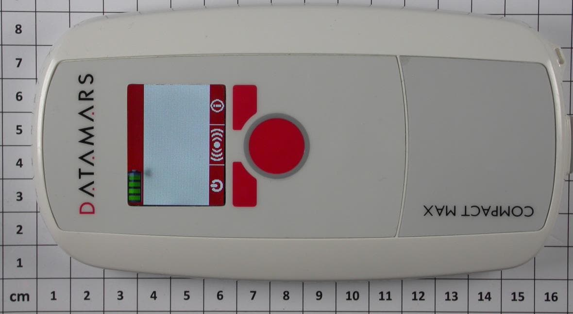
NDX-COMPACTMAX
Aug 17, 2014RFID handheld reader for animal indentification
Equipment Class
DCD - Part 15 Low Power Transmitter Below 1705 kHz
NDX-OMNIMAX
Jan 19, 2014RFID handheld reader for livestock applications
Equipment Class
JBP - Part 15 Class B Computing Device Peripheral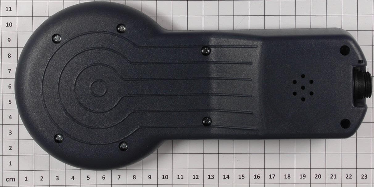
NDX-TRACKING1
Dec 16, 2013RFID handheld reader for livestock applications
Equipment Class
JBP - Part 15 Class B Computing Device Peripheral