NP42424096-001T-96SR 900MHz Transceiver/Modem
CalAmp Wireless Networks Corporation
Click to zoom
Application Details
- Equipment Class
- TNB - Licensed Non-Broadcast Station Transmitter
- Date of Grant
- Jul 14, 1999
- Application Purpose
- Original Equipment
- Date of Application
- Sep 09, 1998
- Equipment Note
- T-96SR 900MHz Transceiver/Modem
- Frequency Range
- 929.00000000 - 930.00000000
- Country
- United States
Documents & Files
Document Text
Text extracted from the exhibit documents filed with the FCC. Open a document above to read the original.
Users Manual
-1 April 1997 Part No. 001-3492-001 3492 Synthesized 900 MHz Transceiver Service Manual First Printing June 1997 Part No. 001-3492-0016-97mwpPrinted in U.S.A. -3 April 1997 Part No. 001-3492-001 3492 SYNTHESIZED 900 MHZ TRANSCEIVER SERVICE MANUAL Copyright 1997 by the Johnson Data Telemetry Corporation. The Johnson Data Telemetry Corporation designs and manufactures radios and radio modems to serve a wide variety of data communication needs. The Johnson Data Telemetry Corporation produces equipment for the fixed data market including SCADA systems for utilities, petrochemical, waste and fresh water management markets and RF boards for OEM applications in the Radio Frequency Data Capture market. In addition, the Johnson Data Telemetry Corporation provides wireless commu- nication solutions to the mobile data market serving public safety, utilities and industrial users. DATA TELEMETRY PRODUCT WARRANTY The manufacturer's warranty statement for this product is available from your product supplier or from the Johnson Data Telemetry Corporation, 299 Johnson Avenue, PO Box 1733, Waseca, MN 56093-0833. Phone (507) 835-8819. WARNING This device complies with Part 15 of the FCC rules. Operation is subject to the condition that this device does not cause harm- ful interference. In addition, changes or modification to this equipment not expressly approved by the Johnson Data Teleme- try Corporation could void the user's authority to operate this equipment (FCC rules, 47CFR Part 15.19). DO NOT allow the antenna to come close to or touch, the eyes, face, or any exposed body parts while the radio is transmitting. DO NOT operate the radio near electrical blasting caps or in an explosive atmosphere. DO NOT operate the radio unless all the radio frequency connectors are secure and any open connectors are properly termi- nated. DO NOT allow children to operate transmitter equipped radio equipment. SAFETY INFORMATION Proper operation of this radio will result in user exposure below the Occupational Safety and Health Act and Federal Commu- nication Commission limits. The information in this document is subject to change without notice. ™ Johnson Data Telemetry is a trademark of the Johnson Data Telemetry Corporation. 1 TABLE OF CONTENTS 1GENERAL INFORMATION 1.1SCOPE OF MANUAL. . . . . . . . . . . . . . . . . . . . . . . . . . . . . . . . . . . . . . . . . . . . . . . . . . . . . . . . . . . . . . . . . . . . . . . 1-1 1.2EQUIPMENT DESCRIPTION. . . . . . . . . . . . . . . . . . . . . . . . . . . . . . . . . . . . . . . . . . . . . . . . . . . . . . . . . . . . . . . . 1-1 GENERAL. . . . . . . . . . . . . . . . . . . . . . . . . . . . . . . . . . . . . . . . . . . . . . . . . . . . . . . . . . . . . . . . . . . . . . . . . . . . . . . . . 1-1 DL3492 WITH LOADER BOARD. . . . . . . . . . . . . . . . . . . . . . . . . . . . . . . . . . . . . . . . . . . . . . . . . . . . . . . . . . . . . . 1-1 DL3492 WITH MODEM. . . . . . . . . . . . . . . . . . . . . . . . . . . . . . . . . . . . . . . . . . . . . . . . . . . . . . . . . . . . . . . . . . . . . . 1-2 DM3492 SYNTHESIZER PROGRAMMING . . . . . . . . . . . . . . . . . . . . . . . . . . . . . . . . . . . . . . . . . . . . . . . . . . . . . 1-2 1.3TRANSCEIVER IDENTIFICATION . . . . . . . . . . . . . . . . . . . . . . . . . . . . . . . . . . . . . . . . . . . . . . . . . . . . . . . . . . 1-2 1.4ACCESSORIES . . . . . . . . . . . . . . . . . . . . . . . . . . . . . . . . . . . . . . . . . . . . . . . . . . . . . . . . . . . . . . . . . . . . . . . . . . . . 1-2 1.5PART NUMBER BREAKDOWN . . . . . . . . . . . . . . . . . . . . . . . . . . . . . . . . . . . . . . . . . . . . . . . . . . . . . . . . . . . . . 1-2 1.6FACTORY CUSTOMER SERVICE. . . . . . . . . . . . . . . . . . . . . . . . . . . . . . . . . . . . . . . . . . . . . . . . . . . . . . . . . . . 1-3 1.7PRODUCT WARRANTY. . . . . . . . . . . . . . . . . . . . . . . . . . . . . . . . . . . . . . . . . . . . . . . . . . . . . . . . . . . . . . . . . . . . 1-3 1.8REPLACEMENT PARTS. . . . . . . . . . . . . . . . . . . . . . . . . . . . . . . . . . . . . . . . . . . . . . . . . . . . . . . . . . . . . . . . . . . . 1-3 1.9FACTORY RETURNS . . . . . . . . . . . . . . . . . . . . . . . . . . . . . . . . . . . . . . . . . . . . . . . . . . . . . . . . . . . . . . . . . . . . . . 1-3 2INSTALLATION 2.1PRE-INSTALLATION CHECKS . . . . . . . . . . . . . . . . . . . . . . . . . . . . . . . . . . . . . . . . . . . . . . . . . . . . . . . . . . . . . 2-1 2.2INTERFACING WITH DATA EQUIPMENT. . . . . . . . . . . . . . . . . . . . . . . . . . . . . . . . . . . . . . . . . . . . . . . . . . . 2-1 DM3492 (RF Board) . . . . . . . . . . . . . . . . . . . . . . . . . . . . . . . . . . . . . . . . . . . . . . . . . . . . . . . . . . . . . . . . . . . . . . . . . 2-1 3PROGRAMMING 3.1INTRODUCTION . . . . . . . . . . . . . . . . . . . . . . . . . . . . . . . . . . . . . . . . . . . . . . . . . . . . . . . . . . . . . . . . . . . . . . . . . . 3-1 3.2DM3492 SYNTHESIZER DATA PROTOCOL . . . . . . . . . . . . . . . . . . . . . . . . . . . . . . . . . . . . . . . . . . . . . . . . . . 3-1 GENERAL. . . . . . . . . . . . . . . . . . . . . . . . . . . . . . . . . . . . . . . . . . . . . . . . . . . . . . . . . . . . . . . . . . . . . . . . . . . . . . . . . 3-1 SYNTHESIZER DATA. . . . . . . . . . . . . . . . . . . . . . . . . . . . . . . . . . . . . . . . . . . . . . . . . . . . . . . . . . . . . . . . . . . . . . . 3-1 D-WORD CALCULATION (24 BITS). . . . . . . . . . . . . . . . . . . . . . . . . . . . . . . . . . . . . . . . . . . . . . . . . . . . . . . . . . . 3-1 C-WORD CALCULATION (24 BITS). . . . . . . . . . . . . . . . . . . . . . . . . . . . . . . . . . . . . . . . . . . . . . . . . . . . . . . . . . . 3-2 B-WORD CALCULATION (24 BITS). . . . . . . . . . . . . . . . . . . . . . . . . . . . . . . . . . . . . . . . . . . . . . . . . . . . . . . . . . . 3-2 A0-WORD CALCULATION (24 BITS). . . . . . . . . . . . . . . . . . . . . . . . . . . . . . . …
Text truncated - open the document above for the full version.
Users Manual
T-96H Radio Modem Technical Manual version 0.01 PRELIMINARY The entire contents of this manual and the Radio Service Software described in this manual are copyright 1998 by DATARADIO Inc. Copyright DATARADIO Inc. August 1998 part no.: 120 10504-001 i Table of Contents 1.PRODUCT OVERVIEW............................................................................................................................1 1.1INTENDED AUDIENCE.................................................................................................................................1 1.2INTRODUCTION..........................................................................................................................................1 1.3GENERAL DESCRIPTION..............................................................................................................................1 1.4PHYSICAL DESCRIPTION..............................................................................................................................1 1.5CONFIGURATION........................................................................................................................................1 1.6CATALOG NUMBERS...................................................................................................................................2 1.7FACTORY TECHNICAL SUPPORT...................................................................................................................2 1.8PRODUCT WARRANTY................................................................................................................................2 1.9REPLACEMENT PARTS.................................................................................................................................2 1.9.1Factory Repair..................................................................................................................................2 1.10DIAGNOSTICS AND REMOTE COMMANDS.................................................................................................3 1.10.1Addressing....................................................................................................................................3 1.10.2Online Diagnostics.......................................................................................................................3 1.10.3Offline Diagnostics.......................................................................................................................4 1.10.4Remote Commands.......................................................................................................................4 1.11NETWORK CONFIGURATION....................................................................................................................4 1.11.1Basic Network...............................................................................................................................4 1.11.2Network Using T-Base..................................................................................................................5 1.11.3Network Using T-Base Repeater...................................................................................................5 1.11.4Network Using T-96H for Online Diagnostics...............................................................................6 2.FEATURES AND OPERATION................................................................................................................7 1.1OVERVIEW.................................................................................................................................................7 2.1INTENDED AUDIENCE.................................................................................................................................7 2.2FRONT PANEL............................................................................................................................................7 2.2.1LED Indicators.................................................................................................................................7 2.3DTE PORT INTERFACE...............................................................................................................................8 2.3.1RS-232 Inteface Signal Levels...........................................................................................................8 2.3.2Interface Port....................................................................................................................................9 2.3.3Interface Signal Description.............................................................................................................9 2.4CHANNEL SELECTION...............................................................................................................................10 2.5OPERATION..............................................................................................................................................10 2.5.1RTS/CTS Timing.............................................................................................................................11 2.5.2XTAL mode.....................................................................................................................................11 2.5.3Extended Turnoff............................................................................................................................11 3.ADJUSTMENTS AND MAINTENANCE................................................................................................12 1.1OVERVIEW...............................................................................................................................................12 3.1INTENDED AUDIENCE...............................................................................................................................12 3.2EQUIPMENT REQUIRED.................................................................................................................…
Text truncated - open the document above for the full version.
External Photos
PHOTOGRAPHS: RULE PART NUMBER:2.983 (g) SEE ATTACHMENTS
ID Label/Location Info
FCC LABEL: RULE PART NUMBER:2.983 (f)
Operational Description
DESCRIPTION OF CIRCUITRY RULE PART NUMBER:2.983 (d)(10) THEORY OF OPERATION 1.0PURPOSE This report has been prepared to support the application for FCC Type Acceptance PER CODE OF FEDERAL REGULATIONS, TITLE 47, PARTS 2, 90 AND 101 for the transmitter subsystem of the JDT Model 242-3492-XYZ Transceiver. The report presents necessary information concerning electrical circuit description, measured performance and physical construction and configuration. 2.0DL-3492 TRANSCEIVER 2.1GENERAL The main subassemblies of this transceiver include the RF board, and Modem board. The RF board provides frequency modulation and demodulation of the radio frequency signal. The main components of the RF board include the Frequency Synthesizer/VCO, dual conversion superheterodyne receiver, RF exciter/power amplifier, and a Temperature compensated crystal oscillator as a frequency reference. The main components of the modem board include the microprocessor, transmit audio processing circuitry, and receive audio processing circuitry. A block diagram of the transceiver is located at the end of this section in Figure 2. 2.2TRANSCEIVER CIRCUIT DESCRIPTION The transmitter produces a nominal RF output power output of 5W at 13.3V DC. Frequency modulation of the transmit signal occurs in the synthesizer. Transmit audio processing circuitry is contained in the modem board. DRIVER (Q500) The VCO RF output signal is applied to R846, R847 and R848 that form a resistive splitter for the receive first local oscillator and the transmitter. The VCO signal is then applied to a 50 ohm pad formed by R500, R501, and R502. The RF signal is applied to Q500 which provides amplification and additional isolation between the VCO and transmitter. Biasing for this stage is provided by R503 and L500, C505 provides RF decoupling. The RF signal is then applied to the power amplifier module Q500. FINAL (U510) The RF signal from Q500 is applied to the input port of the RF power amplifier module, U510, which provides 5 watts (nominal) at the antenna connector J501. U510 operates on an input voltage from 10- 16Vdc. POWER CONTROL (U130C) Power control is provided by U520, U130, Q520 and a stripline directional coupler. The power is adjust by Power Set Control R525 which provides a reference voltage to U130C. U130C drives Q520 and PA module U510. The stripline directional coupler is connected to a forward RF peak detector formed by R535, CR520, C531 and U520A. The other end of the stripline directional coupler is connected to a reverse RF peak detector formed by R593, CR592, C593 and U520B. If the power output of U510 decreases due to temperature variations, etc., the forward peak detector voltage decreases. The detector voltage drop is buffered by U520A and applied to inverting amplifier U130C which increases the forward bias on Q520. The increased bias voltage on Q520 increases the power output level of U510. If the power output of U510 increases, the forward peak detector voltage increases and U130C decreases the forward bias on Q520. The decreased bias voltage on Q520 decreases the output power of U510. The output of CR520 and CR592 are applied to U520. If the output of either buffer increases, the increase is applied to the inverting input of U130C. The output of U130C then decreases and Q520 decreases the input voltage to U510 to lower the power. The control voltage is isolated from RF by ferrite bead EP513 and C513 decouples RF. The forward/reverse power voltages from U520A/B are also applied to U913/U912 for outputs on J201. LOW PASS FILTER The low-pass filter consists of L540, C541, L541, C542, L542, C543, and C544. The filter attenuates spurious frequencies occurring above the transmit frequency band. The transmit signal is then fed through the antenna switch to antenna jack J501. ANTENNA SWITCH (CR540, CR541) The antenna switching circuit switches the antenna to the receiver in the receive mode and the trans- mitter in the transmit mode. In the transmit mode, +9V is applied to L543 and current flows through diode CR540, L544, diode CR541 and R540. When a diode is forward biased, it presents a low impedance to the RF signal; conversely, when it is reverse biased (or not conducting), it presents a high impedance. Therefore, when CR540 is forward biased, the transmit signal has a low-impedance path to the antenna through coupling capacitor C546. L544, and C552 form a discrete quarter- wave line. When CR540 is forward biased, this quarter-wave line is effectively AC grounded on one end by C552. When a quarter- wave line is grounded on one end, the other end presents a high impedance to the quarter-wave frequency. This blocks the transmit signal from the receiver. C545 and C551 matches the antenna to 50 ohms in transmit and receive. TRANSMITTER KEY-UP CONTROL Q130, Q131, and Q132 act as switches which turn on with the RX_EN line. When the line goes low Q130 is turned off which turns Q131 on turning Q132 on. This applies 13.3V to U130 before the TX_EN line goes high. U130A/B provides the key-up and key-down conditioning circuit. C116 and R117 provide a ramp up and ramp down of the 9.0TX during key-up and key-down which reduces load pull of the VCO during key-up. The conditioning provides a stable 5.5V output by balancing the 5.5V reference with the 5.5V regulated supply. The output on U130B, pin 7 is applied to comparator U130D, pin 12, the non- inverting input. The output of U130D, pin 14 is applied to the base of current source Q135. The output of Q135 is on the emitter and is applied back to the inverting input of comparator U130D, pin 13. A decrease or increase at U130D, pin 13 causes a correction by U130D to stabilize the 9V transmit output. R140/141 establish the reference voltage on U130D, pin 13. C143 and C144 provide RF decoupling and C145 stabilizes the output. The 9V transmit voltage is then distributed to the circuits. 2.3POWER SUPPLIES REGULATED +9.6V The RF enable signal applied on J201, pin 5 and to the base of Q110 turning th…
Text truncated - open the document above for the full version.
Parts List/Tune Up Info
008-4096-001 Page 1 of 70 . TRANSISTOR, DIODE, AND IC FUNCTIONS RULE PART NUMBER:2.983 (d)6) DL-3492 TRANSCEIVER Reference Designator FunctionJDEC or Vendor Type CR101ATCXO VaractorBB639 CR200Protection DiodeMMBD6050LT1 CR2402nd LO VaractorBB535 CR520Power ControlMMBD701LT1 CR540Antenna SwitchMMBV3401 CR541Antenna SwitchMMBV3401 CR592Power ControlMMBD701LT1 CR840VCO VaractorBB535 Q100Receive Enable SwitchMUN5213T1 Q101ATCXO OscillatorMMBT3904 Q101Receive Enable SwitchMUN5114T1 Q102ATCXO BufferMMBT3904 Q110RF Enable SwitchMUN5213T1 Q130TX Enable SwitchMUN5213T1 Q131TX Enable SwitchMUN5213T1 Q132TX Enable SwitchMUN5114T1 Q133TX Enable SwitchMUN5213T1 Q134TX Enable SwitchMUN5114T1 Q135TX Enable SwitchPZT2222AT1 Q200RF Amplifier BiasMSB1218-RT1 Q201Low Noise RF AmplifierNE85633 Q2111st LO MixerNE25118 Q2402nd LO BufferMMBT918 Q2602nd LO AmplifierNE85633 Q2612nd LO Amplifier BiasMSB1218-RT1 Q500PA DriverMSA2111 Q520RF Power AmplifierPZT2222AT1 Q800TCXO Level AmplifierMSD1819A-RT1 Q840Synthesizer EnableMUN5213T1 Q841Tx Pin shift PositiveMUN5213T1 Q842TxPin shift NegativeMUN5213T1 Q843Lowband pin shift PositiveMUN5213T1 Q844Lowband pin shift NegativeMUN5213T1 Q845VCOMSD1819A-RT1 Q911Diagnostics EnableMMBT3904 U1105.5 Volts RegulatedTK11900M U1119.6 Volts RegulatedTK11900M U130Power ControlMC33174D U2302nd If/Demodulator/LimiterSA676DK U5106W Pwr module, 900 MHzBGY114E U520Power ControlMC33172D U800FRACTIONAL-N SynthesizerSA7025 U840Shist register 8-STG SOIMC14094 U900TLC5620ID quad 8 bit dacTLC5620ID U901Shift register 8-STG SOIMC14094 U9023 2CH analog mux/de-muxMC14053 008-4096-001 Page 2 of 70 . TRANSISTOR, DIODE, AND IC FUNCTIONS (continued) RULE PART NUMBER:2.983 (d)6) HNET MODEM Reference designatorFunctionType CZ1Transient Voltage Suppressor 5.6v, 0805VC080505A150 CZ2Transient Voltage Suppressor 5.6v, 0805VC080505A150 CZ3Transient Voltage Suppressor 14v, 0805VC080514A300 CZ6Transient Voltage Suppressor 14v, 0805VC080514A300 CZ7Transient Voltage Suppressor 14v, 0805VC080514A300 CZ8Transient Voltage Suppressor 14v, 0805VC080514A300 CZ9Transient Voltage Suppressor 14v, 0805VC080514A300 CZ10Transient Voltage Suppressor 14v, 0805VC080514A300 CZ11Transient Voltage Suppressor 14v, 0805VC080514A300 CZ12Transient Voltage Suppressor 14v, 0805VC080514A300 CZ4Transient Voltage Suppressor 5.6v, 0805VC080505A150 CZ5Transient Voltage Suppressor 5.6v, 0805VC080505A150 D1reverse power supply protection1N4001 D2reference settingBAV99LT1 D3TTL input protectionBAV99LT1 D4TTL input protectionBAV99LT1 D5TTL input protectionBAV99LT1 D6negative peak detectorMBD301LT1 D7positive peak detectorMBD301LT1 D8DIODE,ZENER 4.7vBZX84C4V7LT1 DS1Led, Narrow Beam, YellowHLMP-6400-010 DS2Led, Narrow Beam, RedHLMP-6000-010 DS3LED, Narrow Beam, GreenHLMP-6500-010 Q1LED SwitchMMBT3904LT1 Q2LED SwitchMMBT3904LT1 Q3LED SwitchMMBT3904LT1 Q4phase peak shape formatterMMBT3904LT1 Q5phase peak shape formatterMMBT3904LT1 U1RS-232 Driver/Receiver 5vMC145407DW U2Data Set (sync/async) InterfaceMC145428DW U4Undervoltage Sensing CircuitMC33064D U5Microprocessor ,QFP-8068HC711K4FU U6CPLD 64 Macrocell, Digital ModemPZ5064-I12A44 U7Dual , Op AmpLMC6484AIM U8Quad, Op AmpTLC2274I U9Digital PotentiometerAD8402AR50 U10Quad, Op AmpTLC2274I U11Analog Multiplexers/DemultiplexersMC74HC4053D U12Filter, Linear Phase Low PassLTC1069-7 U13Regulator,Micropower VoltageLP2951CD U14Regulator,Micropower VoltageLP2951CD 008-4096-001 Page 3 of 70 . TRANSMITTER TUNE UP PROCEDURE RULE PART NUMBER:2.983 (d)(9) TRANSMITTER TUNE UP PROCEDURE 1. Connect the transceiver to be aligned to a DC power source. A DC current meter capable of measuring at least 2.5 Amps should be connect in line with the DC source. Connect the output of the transceiver through a watt meter and into a 50 ohm dummy load. 2. Load the synthesizer with the center channel frequency. 3. Key the transmitter and make certain that the supply voltage at the RF board is 13.3 VDC. (Do not transmit for extended periods of time. ) 4. Adjust C525 clockwise for 5.0 Watts of output power. 5. Check the power levels on the low and the high frequencies for 5.0 Watts +/- 1 Watt.
Schematics
10pF C531 51 R538 C809 6.8pF C553 2pF 120nH L240 Z200 OUTIN COM Z201 OUTIN COM 22pF C201 MMBD6050 70V CR200 MMBV3401 35V CR541 MMBV3401 35V CR540 MMBD701LT1 50V CR531MMBD701LT1 50V CR530 5nH L544 1uH L543 8nH L542 12.5nH L541 8nH L540 1uH L500 10nH L263 10nH L262 2.7nH L261 8.2nH L260 270nH L241 L211 15nH 22nH L210 8.2nH L201 2.2nH L200 TP800 TP240 MH513MH512MH511MH510 MH105 MH104 MH103 MH102 MH101 C842 4.7 1 C821 1 C815 1 C519 1 C517 1 C516 1 C514 1 C252 47 C240 1 C145 1 C134 1 C132 1 C120 1 C119 1 C112 1 C110 1 C101 C223 1.5-5pF 220K R818 100K R814 100K R525 1K R914 47K R913 47K R912 10K R911 10k R901 10k R900 24 R849 24 R848 24 R847 24 R846 4.7k R845 10K R844 3.9K R843 10K R842 3.9K R841 R840 10K 10K R823 18K R822 10 R821 10K R820 68K R819 10K R817 39K R816 120k R815 16K R813 4.7k R812 51 R811 4.7k R810 10K R809 4.7K R808 R806 20 R805 6.8K R804 6.8K R803 6.8K R802 4.7k R801 4.7k R800 4.7k 47k R541 100 R540 51 R537 1k R536 51 R535 1k R534 JIC R533 10k R532 10 R531 JIC R530 10k R529 10 R528 10K R527 10k R526 100K R522 10k R521 470 R520 470 R504 470 R503 270 R502 18 R501 270 R500 8.2K R267 100K R266 39K R265 12K R264 220 R263 39K R262390 R261 2.2k R260 4.7k R250 JIC R249 330 R248 330 R247 100k R246 R245 1k 10 R244 22k R243 68K R242 75K R241 100 R240 7.5K R234 33K R233 39k R232 2.4K R231 3.3k R230 1K R223 160 R215 10K R214 1K R213 10 R212 2.2k R205 JIC R204 39K R203 300 R202 39K R201 12K R200 10k R148 5.6k R141 3.6k R140 470 R139 10k R138 150k R137 150k R136 10k R135 10k R134 43K R133 22k R132 1k R131 100k R130 15k R114 100k R113 15k R112 51K R111 100k R110 0.01 C903 0.01 C902 0.01 C901 0.01 C900 0.01 C856 0.01 C855 0.01 C854 22pF C853 22pF C852 22pF C851 22pF C850 0.01 C847 0.01 C846 0.01 C845 0.01 C844 0.01 C843 22pF C8410.01 C840 10pF C823 22pF C822 0.0039 C820 0.0039 C819 0.039 C818 100pF C817 22pF C816 C814 22pF 22pF C813 22pF C812 22pF C811 22pF C810 1.5pF C808 22pF C807 0.01 C806 0.01 C805 0.01 C804 22pF C803 0.01 C802 22pF C801 0.01 C800 10pF C552 2.4pF C551 10pF C550 0.01 C549 68pF C548 22pF C547 22pF C546 2.7pF C545 3.3pF C5443.9pF C543 4.7pF C542 5.6pF C541 22pF C540 10pF C534 0.01 C533 0.01 C530 22pF C529 22pF C528 22pF C527 0.01 C526 JIC C525 22pF C524 0.01 C523 22pF C522 22pF C521 0.01 C520 22pF C518 22pF C515 22pF C513 22pF C512 22pF C511 22pF C510 22pF C506 22pF C505 22pF C504 10pF C503 68pF C502 0.01 C501 22pF C500 1.8pF C270 0.01 C26922pF C268 22pF C267 22pF C266 5.6pF C265 C264 0.01 22pF C263 22pF C262 22pF C261 JIC C260 100pF C254 0.01 C253 0.01 C251 0.01 C250 0.1 C249 0.01 C248 100pF C247 0.01 C246 47pF C245 0.01 C244 56pF C243 22pF C242 0.01 C241 0.01 C237 0.01 C236 10pF C235 0.01 C234 0.01 C233 0.01 C232 0.01 C231 0.01 C230 0.01 C228 0.01 C227 47pF C226 0.01 C225 2.4pF C224 27pF C221 27pF C220 22pF C219 22pF C218 0.01 C217 JIC C215 39pF C214 2.2pF C213 22pF C211 0.01 C210 22pF C207 2.2pF C206 JIC C205 0.01 C204 0.01 C202 22pF C200 22pF C182 22pF C181 22pF C180 22pF C179 C178 22pF 22pF C177 22pF C176 22pF C175 C174 22pF C173 22pF C172 22pF C171 22pF C170 22pF 22pF C146 22pF C144 0.01 C143 22pF C142 0.0082 C141 0.01 C140 0.1 C139 22pF C138 0.01 C137 22pF C136 22pF C135 0.01 C133 22pF C131 22pF C130 22pF C123 22pF C122 0.01 C118 0.01 C117 0.01 C116 0.01 C115 22pF C114 22pF C113 22pF C111 22pF C100 3.3pF C203 L230 680uH PZT2222AT1 Q135 4 1 2 3 U130-4 MC33174D 14 12 13 U130-2 MC33174D 7 5 6 80ohm EP130 U130-1 MC33174D 2 11 GND 4 PWR3 1 Q134 MUN5114T1 Q133 MUN5213T1 Q132 MUN5114T1 Q131 MUN5213T1 Q130 MUN5213T1 J501 1 U111 2 CONTROL 5 GND 4 VOUT 1 BYPASS 3 FEEDBACK 6 VIN U110 2 CONTROL 5 GND 4 VOUT 1 BYPASS 3 FEEDBACK 6 VIN Q110 MUN5213T1 Q101 MUN5114T1 Q100 MUN5213T1 U520 MC33172D 7 5 6 MC33172D U520 1 2 4 GND 8 PWR 3 U130-3 MC33174D 8 10 9 L222 6 2 4 8 5 1 3 7 L212 6 2 4 8 5 1 3 7 60ohm EP512 U510 2 VS1 3 VCC 4 VS2 5 RF_OUT 1 RF_IN 80ohm EP511 PZT2222AT1 Q520 4 1 2 3 80ohm EP513 80ohm EP510 Q500 MSA2111 42 31 VCO_3492 A840 10 NC10 7 MOD_ADJ 20 -2.5V 1 TXPINSH_POS 13 GND13 6 NC6 18 LOWBAND_NEG 17 LOWBAND_POS 19 CTRL 9 SYNTH_OUT 21 GND21 5 NC5 2 GND2 11 NC11 14 GND14 22 TXPINSH_NEG 16 9V_FIL 25 GND25 24 GND24 23 GND23 3 MOD_IN 12 RF_OUT 8 GND8 4 GND4 15 GND15 Q845 MSD1819A CR840 2.1-18.7pF BB535 Q842 MUN5213T1 Q840 MUN5213T1 Q844 MUN5213T1 Q843 MUN5213T1 Q841 MUN5213T1 U840 14 Q4 13 Q5 11 Q7 10 _QS 9 QS 4 Q0 5 Q1 6 Q2 7 Q3 3 CLK 1 STR 15 OE 8 GND 2 SER 12 Q6 16 VCC 17.5MHz Y800 18 GND18 19 GND19 15 GND15 17 GND17 20 GND20 14 VCC 7 GND7 1 VC_MOD_IN 16 GND16 8 RF_OUT U800 12 GND12 19 TEST 4 GND4 10 AUXIN 7 VCC7 6 _RFIN 18 LOCK 13 PHI 14 PHP 17 RF 11 PHA 1 CLOCK 2 DATA 8 REF_IN 9 RA 15 VCC15 5 RFIN 3 STROBE 20 VCC20 16 RN Q800 MSD1819A HEF4053 U902 16 VDD 11 S 7 VEE 12Y0 14Z 13Y1 8 VSS 6 _E U901 14 Q4 13 Q5 11 Q7 10 _QS 9 QS 4 Q0 5 Q1 6 Q2 7 Q3 3 CLK 1 STR 15 OE 8 GND 2 SER 12 Q6 16 VCC HEF4053 U902 4Z 3Y1 9 S 5Y0 HEF4053 U902 15Z 1Y1 10 S 2Y0 Q911 2N3904 U900 13 LDAC 8 LOAD 12 DACA 7 CLK 10 DACC 11 DACB 14 VCC 2 REFA 1 GND 9 DACD 3 REFB 5 REFD 6 DATA 4 REFC J201-9 9 J201-14 14 J201-13 13 J201-12 12 J201-11 11 J201-10 10 J201-8 8 J201-7 7 J201-6 6 J201-5 5 J201-4 4 J201-3 3 J201-2 2 J201-1 1 Q240 MMBT918 CR240 2.6-38.7pF BB639 U230 2 RF_IN- 14 LIMITER_IN 9 RSSI_FB 4 OSCB 3 OSCE 13 LIMITER_DEC2 17 IF_AMP_DEC1 18 IF_AMP_IN 19 IF_AMP_DEC2 20 MIXER_OUT 5 RSSI_OUT 7 AUDIO_FB 8 AUDIO_OUT 10 QUAD_IN 16 IF_AMP_OUT 12 LIMITER_DEC1 1 RF_IN+ 11 LIMITER_OUT 6 VCC6 15 GND15 Z231 450kHz OUT IN COM Z230 450kHz OUT IN COM 45MHz Z221 2 13 45MHz Z220 2 13 Q261 MSB1218A 1 2 3 NE85633 Q260 Q211 3 2 1 4 Q201 NE85633 Q200 MSB1218A 1 2 3 13.6_SW 13.6_SW 13.6_SW 9.0TX 9.0TX 9.0TX 9.0TX 9.6REG 9.6REG 9.6REG 17.5_TCXO 17.5_TCXO SYNTH_DATA SYNTH_DATA TX_PSET TX_PSET V_REV V_REV V_FWD V_FWD DAC_POW_CTRL DAC_POW_CTRL MOD_ADJ MOD_ADJ P_SET P_SET DIAG DIAG DIAG DIAG_EN DIAG_EN DIAG_EN CLOCK CLOCK CLOCK CLOCK CLOCK DATA DATA DATA DATA SYNTH_EN SYNTH_EN SYNTH_EN SYNTH_EN SYNTH_EN LOCK_DETECT LOCK_DETECT LOCK_DETECT MOD_IN MOD_IN RF_ENABLE RF_ENABLE RX_EN RX_ENRX_EN TX_EN TX_EN 13.6_V 13.6_V 13.6_V 13.6_V 13.…
Text truncated - open the document above for the full version.
Schematics
Q4 MMBT3904 3 1 2 R45 470K R32 10K R25 10K R33 220K R65 1K C26 104 C32 104 C13 102 C34 102 R53 6.8K U11C 74HC4053D Z0 5 Z1 3 C 9 Z 4 VCC 16 EN 6 VEE 7 GND 8 R64 100K R62 100K C33 104 R42 470K R27 220K C23 103 R36 470K R55 10K R46 10K Q5 MMBT3904 3 1 2 C29 224 35V_A + C22 224 35V_A + TP4 U9C AD8402AR50 SDI 8 CLK 9 /CS 7 DGND 1 AGND 5 /SHDN 6 /RS 10 VDD 11 D6 MBD301 1 3 U7C LMC6484 10 9 8 - + U10D TLC2274 12 13 14 - +U10A TLC2274 3 2 1 - + U7B LMC6484 5 6 7 - + C25 104 C24 104 C31 104 C30 104 C39 104 C35 104 R26 10K U8B TLC2274 5 6 7 - + R29 10K R30 10K U8C TLC2274 10 9 8 - + R37 68K R35 10K U7A LMC6484 3 2 1 4 11 - + + - U10B TLC2274 5 6 7 - + U9B AD8402AR50 32 4 A2B2 W2 U8A TLC2274 3 2 1 - + R40 33K R50 10K U11A 74HC4053D X0 12 X1 13 A 11 X 14 R68 1K C37 102 U10C TLC2274 10 9 8 4 11 - + + - R58 47K R59 100K D7 MBD301 1 3 U7D LMC6484 12 13 14 - + R71 1K C45 224 35V_A + U11B 74HC4053D Y0 2 Y1 1 B 10 Y 15 U9A AD8402AR50 1314 12 A1B1 W1 R49 68K R28 10K R34 470K R24 1K U8D TLC2274 12 13 14 4 11 - + + - U12 LTC1069-7 AGND 1 V+ 2 VIN 4 CLK 5 V- 7 VOUT 8 GND 3 GND 6 AVCC +2.5V AVCC DVCC AVCC +2.5V AVCC AVCC AVCC +2.5V AVCC +2.5V AVCC +2.5V +2.5V +2.5V +2.5V AVCC +2.5V DET_AUDIO MOD PDRST NEG_PEAK TEST_AUDIO RSSI_IN RSSI_DIR RSSI RSSI_OUT CLK DIGIPOT_EN DATA POS_PEAK RXS SLICER TXA FILTER_CK TX_EN DATARADIO INC. B No reproduction or distribution without approval. This information is the property of DATARADIO INC. and is confidential 1 2 3 4 5 ABCDEFGH 1 2 3 4 5 ABCDEFGH COPYRIGHT C 1985-97 : DATARADIO INC. H-NET 2/3 C.LAMBERT ANALOG SECTION 215-03280-00F (1) (1) (1) (1) (3) (3) (1) (3) (3) (1) (3) (1) (1) U7U8U10U9U11U12 (1) (1) (1) (1) (1) SEE NOTE NOTE:R59 REMOVED FOR TBASE DIAGOSTIC BOARD FPRE-PRODUCTION971224 EFOR NEW LAYOUT971120 REVDESCRIPTIONDATE Design …
Text truncated - open the document above for the full version.
Contact Information
Applicant
Russell Cook(Director of Engineering)
Technical Specifications
| # | Rule Parts | Frequency Range | Power Output | Emission | Tolerance |
|---|---|---|---|---|---|
| 4 | 9 | 929 MHz - 930 MHz | 5 W | 15K3F1D | 1.5 ppm |
Other Applications from CalAmp Wireless Networks Corporation
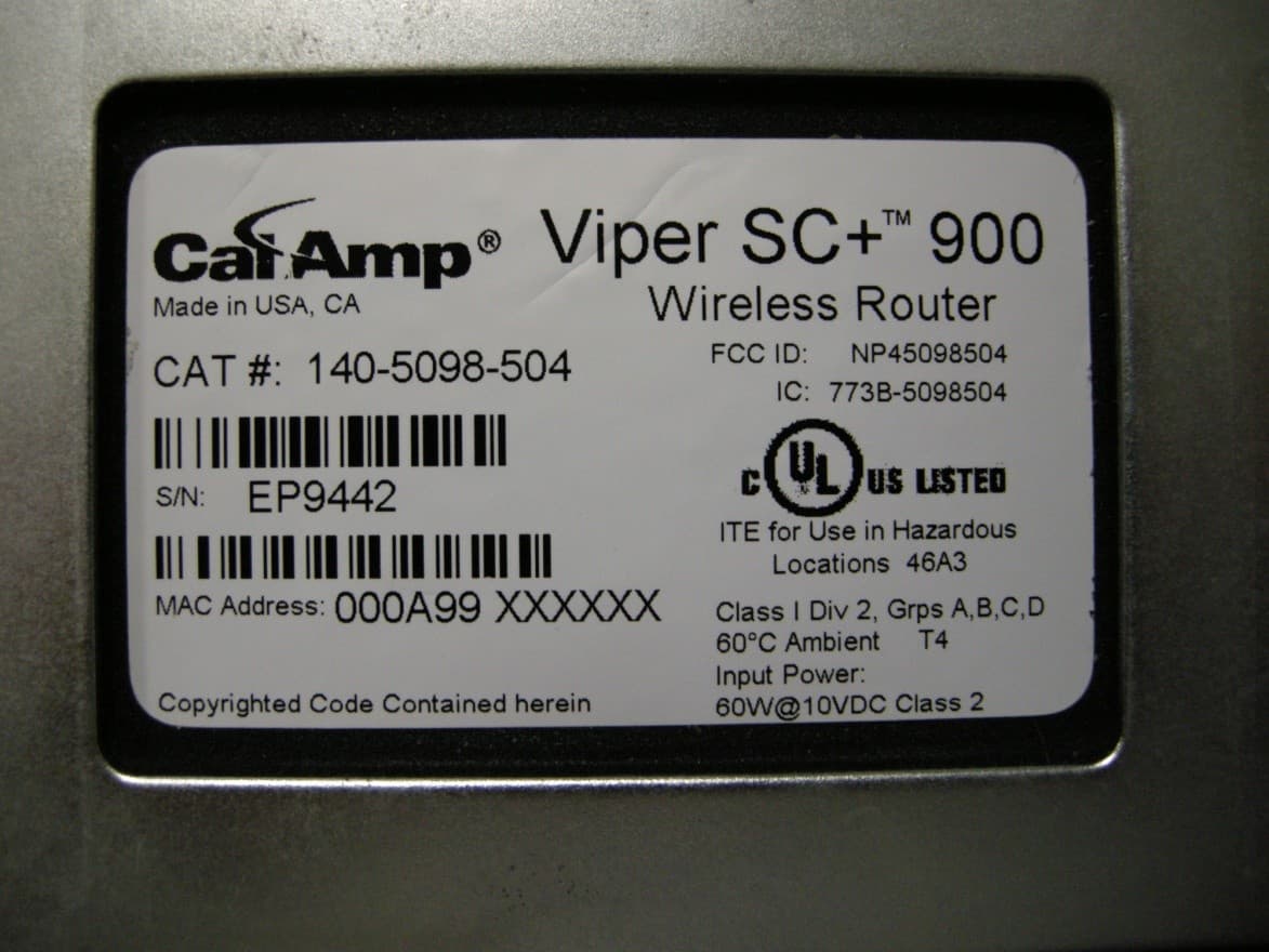
NP45098504
Sep 10, 2013Viper SC+ 928-960 MHz
Equipment Class
PCB - PCS Licensed Transmitter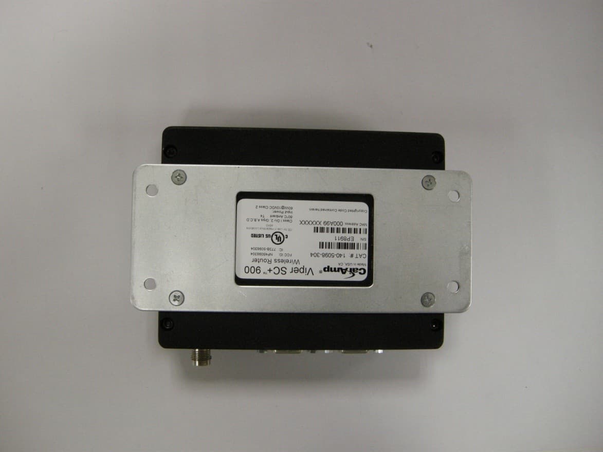
NP45098304
Aug 29, 2013VIPER SC+ 900 VHF 880-902 MHZ
Equipment Class
PCB - PCS Licensed Transmitter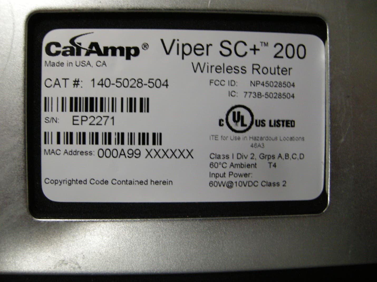
NP45028504
Aug 22, 2013VIPER SC+ 200 VHF 215-240MHZ
Equipment Class
TNB - Licensed Non-Broadcast Station Transmitter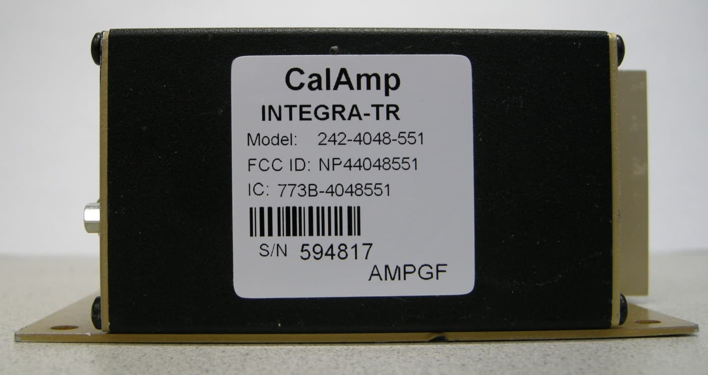
NP44048551
May 09, 2013UHF Wireless Radio Modem
Equipment Class
TNB - Licensed Non-Broadcast Station Transmitter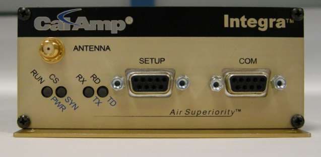
NP44048351
Apr 25, 2013UHF Wireless Radio Modem
Equipment Class
TNB - Licensed Non-Broadcast Station Transmitter