NP4MCUA5Q
CalAmp Wireless Networks Corporation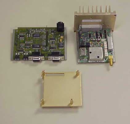
Click to zoom
Application Details
- Equipment Class
- TNB - Licensed Non-Broadcast Station Transmitter
- Date of Grant
- Aug 06, 2001
- Application Purpose
- Original Equipment
- Date of Application
- Jun 10, 2001
- Frequency Range
- 132.00000000 - 174.00000000
- Country
- United States
Documents & Files
Document Text
Text extracted from the exhibit documents filed with the FCC. Open a document above to read the original.
Users Manual
Integra T e c h n i c a l M a n u a l Version: Integra-TR S e r v i c e INTEGRA-TR WIRELESS MODEM Part No. 242-40V8-XYZ Copyright 1999 by Dataradio Inc. Part Number: 001-4008-101/102 Revision 5 June 2001 Dataradio COR Ltd. designs and manufactures radios and wireless modems to serve a wide variety of data communication needs. Dataradio produces equipment for the fixed data market including SCADA systems for utilities, petrochemical, waste and fresh water management markets and RF boards for OEM applications in the Radio Frequency Data Capture market. PRODUCT WARRANTY The manufacturer's warranty statement for this product is available from Dataradio COR, Ltd. 299 Johnson Avenue, Box 1733, Waseca, MN 56093-0833. Phone (507) 833-8819. The information in this document is subject to change without notice. is a trademark of DATARADIO, Inc. SECTION 1 PRODUCT OVERVIEW 1-1 001-4008-101/102 1.1 SCOPE OF MANUAL This document provides the information required for the operation and preventive maintenance of the D ATARADIO Integra-TR wireless modem. This manual is intended for system designers, installers and maintenance technicians 1.2 GENERAL DESCRIPTION Integra-TR is a high-speed transparent wireless modem. It is FCC refarming compliant and designed specifically to fit the needs of SCADA, telemetry and control applications. Integra-TR provides the communication links to data equipment for installations where wired communication is impractical. Integra-TR works with most makes and models of remote terminal units (RTU) and programmable logic controllers (PLC) and their protocols. Configuration settings allow tailoring for a variety of applications. Integra-TR supports: 1. Point to point Master-Remote or Peer-to-Peer configurations in simplex or half-duplex modes. 2. Point to multipoint Master-Remote configuration in simplex or half-duplex modes and offers full-duplex in dual-unit configuration. Settings and connections for these configurations are given later in this manual 1.2.1 CHARACTERISTICS Integra-TR has the following characteristics: z Selectable network speeds of 4800 and 9600 b/s for half channel units as well as 4800, 9600 and 19.200 b/s for full channel units. 2400 or 4800 b/s for quarter channel units z Backward compatible with the Integra-T for bit rate of 4800 and 9600 b/s (full channel units only) z One COM port for connection to DTE. Speed of 300 - 19200 bauds z One Setup port, for configuration and diagnostics (speed fixed to 9600 baud, 8 bit, no parity, 1 stop bit) z Built-in 5-watt transceiver, operating in the VHF, UHF or 900 MHz communications bands. Half-duplex or simplex operation z Fully transparent operation with error-free data delivery z Allows transmission of “break” characters z DOX (Data Operated Transmit) or RTS mode z Stations may be set as “master” or “remote” to prevent remote stations from hearing each other in a simplex RF configuration z Full local and remote diagnostics z Two 8-bit analog inputs (0 - 10V) z Low power consumption modes: “sleep” and “suspend” modes (< 20 mA). z “12 VDC, negative ground” device. 1-2 Part No. 001-4008-101/102 1.2.2 ACCESSORIES AND OPTIONS * For extended-transmit applications, the “TX Time out” timer must be turned off (set to “disable”) via the Field Programming Software. For information on accessories and options, contact your sales representative. In the United States phone 1- 800-992-7774. For international sales, phone 1-952-882-5529 or 1-305-829-4030. 1.2.3 FACTORY MUTUAL NI KIT The Integra-TR with the Factory Mutual NI Kit (DRL part number 023-1000-200) is approved as nonincendive for Class I, Groups ABCD, Division 2, hazardous locations by Factory Mutual Research Corporation. This option includes approval for International Electrotechnical Commission (IEC) Class I, Zone 2. Approved models are labeled with this rating. Only units with the Factory Mutual approved label carry the nonincendive rating. Installation, service, and repair of the FM approved units must be in accordance with the instructions found in this manual and the National Electrical Code (ANSI-NFPA 70) Division 2: Hazardous (classified) Location Incendive Wiring Techniques. Mount the unit in an enclosure or assembly. Route all interconnecting cables (DC power and coaxial) through conduit as specified in the National Electrical Code document referenced above. For further guidance on installation, see ANSI\ISA-RPI2.6: Installation of Intrinsically Safe Systems for Hazardous (Classified) locations. Figure 1-1 FM Approved External Connections AccessoryDRL Part Number Integra-TR Field Programming Kit (includes software and technical manual on CD ROM, and programming cable - DRL part number 697-4008-408) 250-4008-001 SMA Male - BNC Female adapter cable023-3410-098 *Cooling fan - factory option (For extended duty-cycle transmit applications) Catalog number plus “F” suffix. Power cable697-4008-001 Factory Mutual NI Kit023-1000-200 *Full-duplex base station - Y-cable optionContact Technical Service User Interface Cable Data Port Programming Port To Antenna System (SMA Connection) 1-3 Part No. 001-4008-101/102 Figure 1-2 Installation Dimensions 1-4 Part No. 001-4008-101/102 1.2.4 INTEGRA-TR CE Important Notice/Warning on restrictive use in all EU and EFTA member states: This device is a VHF/UHF Radio data transmitter intended for indoor and outdoor use. Operation of this device is subject to end-user licence. The end user is strongly advised to contact the local frequency management authorities to obtain such an end-user licence according to local legislations and frequency allocations. The manufacturer takes no responsibility for any unauthorized use of this device. Avis important/Avertissement au sujet de restrictions d’utilisation applicables à l’intérieur d’un pays membre de l’UE ou de l’AELE : Cet appareil est un émetteur radio opérant en VHF/UHF, d’usage intérieur ou extérieur, utilisé pour la transmission de données. L’opération de cet appareil est assujettie aux te…
Text truncated - open the document above for the full version.
External Photos
Integra-TR DL3422 Engineering Report – Annex C Page 1 of 4 06/11/01 ID Label 1. Label identification and place: right side, closest to power connector. Integra-TR DL3422 Engineering Report – Annex C Page 2 of 4 06/11/01 External Photos 1. Overview: showing left, rear, and top 2. Front view 3. Back View Integra-TR DL3422 Engineering Report – Annex C Page 3 of 4 06/11/01 Internal Photos 1. Top assembly, showing bottom of RF Board and top of Modem. 2. Bottom assembly, showing top of RF Board and bottom of Modem. Integra-TR DL3422 Engineering Report – Annex C Page 4 of 4 06/11/01 3. Exploded view: showing top of modem, top of RF Board, and separating plate.
External Photos
Integra-TR DL3422Engineering Report – Annex CPage 1 of 1 06/22/01 External Photos 1. Overview: showing left, rear, and top 2. Front view 3. Back View
ID Label/Location Info
Integra-TR DL3422Engineering Report – Annex CPage 1 of 1 06/22/01 ID Label 1. Label identification and place: right side, closest to power connector.
Internal Photos
Integra-TR DL3422Engineering Report – Annex CPage 1 of 2 06/22/01 Internal Photos 1. Top assembly, showing bottom of RF Board and top of Modem. 2. Bottom assembly, showing top of RF Board and bottom of Modem. Integra-TR DL3422Engineering Report – Annex CPage 2 of 2 06/22/01 3. Exploded view: showing top of modem, top of RF Board, and separating plate.
Internal Photos
Integra-TR DL3422Engineering Report – Annex CPage 1 of 2 08/02/01 Internal Photos 1. Bottom of RF Board without shields. Integra-TR DL3422Engineering Report – Annex CPage 2 of 2 08/02/01 2. Top of RF Board without shields.
Operational Description
SECTION 6 CIRCUIT DESCRIPTION 6-1 001-4008-101/102 6.1 OVERVIEW Section 6 describes the circuit operation of the logic board. This section is intended for use by engineering and service personnel. 6.2 CIRCUIT DESCRIPTION Refer to Figure 6-1 for the block diagram of the Integra-TR Logic Board. 6.2.1 MICROPROCESSOR CIRCUIT The microprocessor contains two Z84015 CMOS low power Intelligent Peripheral Controllers (IPC). Each IPC is an 8-bit microprocessor integrated with CTC, SIO, PIO Clock Generator Controller and Watch Dog Timer. One of the Z84015s (U17) is used in the normal mode. The other Z84015 (U21) is used in the evaluation mode and only the CTC, SIO and PIO sections are used. The CPU section is disabled. The first Z84015 Clock Generator uses a 19.6608 MHz crystal that provides a CPU clock rate of 9.8304 MHz for both Z84015s. The 9.8304 MHz clock is further divided by 2 to feed all 8 CTC (4 in each Z84015). The 64K-memory space of the Z84015 is divided into two blocks of 32k each. The lower 32K are used for the firmware program and the upper 32K by the CMOS RAM (U18). The memory IC used for the program is a CMOS FLASH (U22) with 1024 sectors of 128 bytes each. The dual Z84015 circuit provides up to 8 Counter Timer Channels (CTC), 4 Serial Input/Output (SIO) and 32 Parallel In-put/Output (PIO) lines. The CPU also provides the clock for the CPLD modem. 6.2.2 RS232 The RS232 IC (U15) is used to interface the application DE-9 connector to the SIO_B section of U17, and the set-up DE-9 connector to the SIO_A section of U21. Two receivers remain enabled in sleep mode to ensure fast wakeup. 6.2.3 MODEM The modem section is used to interface the serial digital data to the transceiver. The CPLD modem IC (U16) with a programmable Raise-Cosine filter (U10) operates in DRCMSK mode at 2400, 4800, 9600, and 19200 bits/sec. It incorporates a 7-bit hardware scrambler and uses Differential (NRZI) encoding in DRCMSK mode to minimize data pattern-sensitivity. An electronic potentiometer U5B 6-2 Part No. 001-4008-101/102 (E-Pot), controlled by CPU U17, is used to set the transmitter deviation by amplitude adjustment of the baseband signal. Electronic potentiometer U5C is also provided to fine adjust the RF carrier frequency. 6.2.4 TRANSMIT & RECEIVE DATA Transmit Data from the RS-232 port is level-shifted to TTL by U15 and passed through the CPU for further processing and conversion from asynchronous to synchronous format. The CPLD modem, U16, takes the digital data stream from SIO-A of the CPU and synthesizes to the constant-amplitude analog baseband signal. The synthesized data stream is filtered by U10, buffered by U9B, and applied to radio module TXA at P1-6. Received signals are applied to the RXA pin on P1-13 and amplified by U3A. U3A gain is set by the electronic potentiometer, U5D, and filtered by U10. The same filter circuit is used for transmission and reception. Two analog multiplexer/demultiplexer gates (U8A and B) controlled by TX_EN line are used for sharing. The filter U10 cut-off frequency is programmable by the CPLD, based on the data rate. The analog signal is buffered by U1D and fed to Peak Detectors U3C, U3D, and U3B, and to slicer circuit U1C via U1B. The raw data is passed to the CPLD modem (U16) for de-scrambling and receive clock recovery. The resulting synchronous bit stream is fed to CPU SIO-A for further processing and conversion to asynchronous format before delivery to the RS-232 driver and to the user port. 6.2.5 INTEGRA-TR A/D AND DIGIPOT An 8 channel, 8-bit successive approximation A/D converter, type ADC0838 (U4), is interfaced to CPU (U17) and Peripheral (U21). CH0 and CH1 are connected to the positive and negative peak detector of the modem section. The software can read the positive or negative value of an RX signal, or using the differential mode, the actual peak-to- peak RX signal value. CH3 is used to measure the radio RSSI signal which was amplified by U7A. CH4 is connected to the radio diagnostic signal (P3-14). This pin is used to output an analog signal corresponding to the power output and the reflected signal. CH5 is connected to U6 (LM50), a temperature sensor with a -40 to +125°C range. CH6 is used to read the SWB+ voltage after proper scaling into the 0-5 V range. CH7 and CH8 are connected to EXT SIGNAL 1 and 2. A 2:1 divider and protection circuit is inserted between both external signals and the A/D. The External Signal (pins 1 and 2) is also connected to U21 at PB6 and PB7 through transistors Q3 and Q4 and can be used for Analog Input or Digital Output. EXT_SIGNAL 2 is also connected to the Rx test point RX-TP through U8A (74HC4066). Under software control, the RX-TP (scaled down by 2) is available on the power connector for trouble-shooting purposes. A 4-channel digital potentiometer type (U5) is used to adjust the RX Signal, TX Modulation, Carrier Frequency and Carrier Detect Threshold. 6-3 Part No. 001-4008-101/102 An 8 channel, 8-bit successive approximation A/D converter, type AD0838 (U9), is interfaced to CPU (U18) and Peripheral (U20). U19 generates a power-on reset for the CPU and U6 is a temperature sensor used by the firmware to compensate for variations in RSSI. The RSSI signal from the transceiver is amplified and filtered by U7A. The signal is compared to a threshold value set by digital potentiometer (U5A). The output of the comparator (U7B) is used to change the hold time of both peak detectors at the beginning of the receive packet. 6.2.6 WAKE-UP CIRCUIT The wake-up circuit for the Integra-TR consists of a 50 ms monostable circuit that is triggered by the rising edge of a Sleep signal from CPU (U17). The falling edge of this 50 ms pulse (end of pulse) is connected to the NMI of the CPU and will wake up the CPU from Sleep mode after 50 ms. When exiting SLEEP mode on a \NMI, the CPU firmware will increment a counter, then return to Sleep until it reaches a limit set by a software parameter. When the programmed count is reached the CPU will w…
Text truncated - open the document above for the full version.
Operational Description
SECTION 4 4-1 Part No. 001-3422-201/202 CIRCUIT DESCRIPTION 4.1 GENERAL 4.1.1 INTRODUCTION The main subassemblies of this transceiver are the RF board, PA module, and TCXO. A block diagram of the transceiver is located in Figure 4-1. The 3422 is available with a reference oscillator stability of ±2.5 PPM. The TCXO (Temperature Compensated Crystal Oscillator) is soldered directly to the RF board. The TCXO is not field serviceable. 4.1.2 SYNTHESIZER The VCO (voltage-controlled oscillator) output signal is the receiver first injection frequency in the Receive mode and the transmit frequency in the Transmit mode. The first injection frequency is 21.45 MHz above the receive frequency. The frequency of this oscillator is controlled by a DC voltage produced by the phase detector in synthesizer chip U811. Channels are selected by programming counters in U811 to divide by a certain number. This programming is performed over a serial bus formed by the Synth Clock, Synth Enable, and Synth Data pins of J201. This programming is performed by user supplied hardware and software (see Section 3). The frequency stability of the synthesizer in both the receive and transmit modes is established by the stability of the reference oscillator described in the preceding section. These oscillators are stable over a temperature range of -30° to +60° C (-22° to +140° F). 4.1.3 RECEIVER The receiver is a double-conversion type with intermediate frequencies of 21.45 MHz / 450 kHz. Varactor tuned LC bandpass filters reject the image, half IF, injection, and other unwanted frequencies. A four-pole crystal filter enhances receiver selectivity. 4.1.4 TRANSMITTER The transmitter produces a nominal RF power output of 5W at 13.3V DC, adjustable down to 1W. Frequency modulation of the transmit signal occurs in the synthesizer. Transmit audio processing circuitry is contained in customer-supplied equipment. Table 4-1 Reference Frequency BandFrequency Band 414.85 MHz Band 617.5 MHz Band 717.5 MHz CIRCUIT DESCRIPTION 4-2 Part No. 001-3422-201/202 4.2 SYNTHESIZER/ VCO The synthesizer output signal (produced by a VCO) is controlled by a DC voltage produced by the phase detector in U811. The phase detector senses the phase and frequency of the two input signals and causes the VCO control voltage to increase or decrease (if they are not the same). The VCO is then “locked” on frequency. Synthesizer programming provides the data necessary for the internal prescaler and counters. One input signal is the reference frequency. This frequency is produced by the 14.85 MHz reference oscillator (TCXO). The other input signal is the VCO frequency. Figure 4-1 U811 Synthesizer Block Diagram CLOCK DATA STROBE Vss RF IN RF IN 64/65/72 PRESCALER MAIN DIVIDERS EM FB 22128 PRNM1NM3 NM2 FRACTIONAL ACCUMULATOR PRESCALER MODULUS CONTROL 3 FMOD NF FB SERIAL INPUT + PROGRAM LATCHESV DD TEST IN REF EM+EA REFERENCE DIVIDER+2+2+2 MAIN MAIN PHASE DETECTOR REFERENCE SELECT 2 SM EM REFERENCE SELECT 2 SA SECONDARY PHASE DETECTOR EA AUXILIARY IN EA AUX 12 NR 12 NAPA AUXILIARY DIVIDER PRESCALER 1/4 NORMAL OUTPUT CHARGE PUMP OUTPUT CHARGE PUMP SPEED-UP OUTPUT CHARGE PUMP INTEGRAL OUTPUT CHARGE PUMP AUXILIARY CN 8 CL 2 CK 4 2 V SSA V DDA LOCK PHA RA PHI PHP RN RF CIRCUIT DESCRIPTION 4-3 Part No. 001-3422-201/202 Figure 4-2 Transceiver Block Diagram 4.2.1 VOLTAGE-CONTROLLED OSCILLATOR The VCO is formed by Q872, several capacitors and varactor diodes, and air wound coil L872. It oscillates at the transmit frequency in transmit mode and first injection frequency in the receive mode (132-174 MHz in transmit and 153.45-195.45 MHz in receive). RF AMP MIXER CRYSTAL FILTER PREDRIVER ANTENNA SWITCH RX AUDIO VCO T/R PS SYNTHESIZER VCO RSSI LOW-PASS FILTER RF OUT RF BPF RF BPF IF / 450 kHz FILTER 1st LO AMP CLV BUFFER/AMPLIFIER RSSI RX OUT TX INY801 TCXO MOD INPUT MOD ADJUST SYNTH OUT RF IN U241 TRANSMITTER RECEIVER +13.6V +4.6V U581A U581B PWR SET DIAG DIAG EN MOD ADJ DIAG DIAG EN TX EN +9V TX RX EN +13.6V SWITCHED CLOCK DATA ENABLE LOCK Q122 Q121 Q801 TEST -2.0V Q501 Q123 +5V DC SHUTDOWN Q511 Q531/U111C CR561/562 V FWD V REV U913C U911 U912 Q131/U131 U141 +9.6V +5.5V Q201/Q202 U531 Q301/Q302 Q231/Q232 21.45 MHz Z231/Z232 Q251 Q101/Q102 U111A/B/D Q124 Q871/Q872Q881/Q882 Q171, Q172, Q173 Q173, Q841 Q842, Q901 AUX IN U811 Q701 CR281/CR282CR281/CR282 CR251 U801 CLOCK DATA U913A U831BU913B 13.6V SWITCHED Q901 REG REG PHP PHA CIRCUIT DESCRIPTION 4-4 Part No. 001-3422-201/202 Biasing of Q872 is provided by R873, R874 and R876. The LC Tank Circuit is formed by C872, C874, C875, L872, and C873 which starts and maintains oscillation. The VCO frequency is controlled in part by DC voltage across varactor diodes CR852, CR853 and CR854. As voltage across a reverse-biased varactor diode increases, its capacitance decreases. Therefore, VCO frequency increases as the control voltage increases. CR852/CR853 and CR854 are paralleled varactors to divide the capacitance and improve linearity. The varactors CR852/CR853 are biased at -2.0V so the control line voltage can operate closer to ground. CR854 is pin shifted in when transmitting to increase the VCO gain in transmit. The control line is isolated from tank circuit RF by choke L852/L853. The amount of frequency change produced by CR852/CR853/CR854 is controlled by series capacitor C854. The -2.0V applied to the VCO is derived from the TCXO frequency that is amplified by Q902, rectified by CR902 and filtered by C912, C917, C918 and C920 and loaded by resistor R919. 4.2.2 VCO AND REFERENCE OSCILLATOR MODULATION Both the VCO and reference oscillator (TCXO) are modulated in order to achieve the required frequency response. The TCXO responds to the lower modulating frequencies approximately 0-200 Hz. The VCO responds to the higher modulating frequencies (200 Hz and above). Potentiometers R825 and R827 set the VCO modulation sensitivity so that it is equal to the reference oscillator modulation sensitivity. The VCO frequency is modulated using a …
Text truncated - open the document above for the full version.
Parts List/Tune Up Info
DL-3422 TUNE-UP PROCEDURE Ref: FCC Part 2 paragraph 2. 1033(c)(9) 1. Connect the transceiver to be aligned to a DC power source. A DC current meter capable of measuring at least 2.5 Amps should be connect in line with the DC source. Connect the output of the transceiver through a watt meter and into a 50 ohm dummy load. 2. Load the synthesizer with the center channel frequency. 3. Key the transmitter and make certain that the supply voltage at the RF board is 13.3 VDC. (Do not transmit for extended periods of time. ) 4. Adjust R535 clockwise for 5.0 Watts of output power. 5. Check the power levels on the low and the high frequencies for 5.0 Watts +/- 1 Watt. DL-3422 ACTIVE CIRCUITS DESCRIPTION Designator Function JEDEC or Vendor Type CR561 Antenna switch MMBV3401 CR562 Antenna switch MMBV3401 CR591 Directional coupler MMBD701LT CR592 Directional coupler MMBD701LT CR851 Pin shift diode MMBV3401 CR852 Rectifier MMBV609 CR853 Rectifier MMBV609 CR861 Varactor BB535E7908 CR862 Varactor BB535E7908 CR901 Varactor BB535E7908 CR902 Rectifier BAV99LT1 Q101 Tx enable MUN5213T1 Q102 Tx enable MUN2114T1 Q121 Rx enable MUN5213T1 Q122 Rx enable MUN5213T1 Q123 Rx enable MUN2114T1 Q124 Soft key up control PZT2222AT1 Q131 5 volt shutdown MUN5213T1 Q171 Pin shift MUN5213T1 Q172 Pin shift MUN2114T1 Q501 RF buffer MSA-2111 Q511 RF driver NE85633 Q531 Power control PZT2222AT1 Q801 Constant voltage source MSD1819A-RT1 Q841 Pin shift MUN5213T1 Q842 Pin shift MUN2114T1 Q871 VCO buffer NE85619-T1 Q872 Oscillator NE85619-T1 Q881 Bias regulator MSB1218A-AT1 Q882 Amplifier NE85633 Q901 Capacitance multiplier MSD1819A-RT1 Q902 Amplifier MMBT918LT1 U111A Soft key up control LMC660AMI U111B Soft key up control LMC660AMI U111C Power control LMC660AMI U111D Soft key up control LMC660AMI U131 Voltage regulator TK11900MTL U141 Voltage regulator TK11900MTL U531 RF power module M57732 U581A V-fwd amp MC33172DT U581B V-rev amp MC33172DT U811 Synthesizer SA7025DK-T Y801 TCXO 14.85 / 17.5 MHz INTEGRA R 210-3315-XXX ACTIVE CIRCUITS DESCRIPTION Designator function Type D1 DIODE, HOT CARRIER, SOT-23 MMBD301LT1 D2 DIODE, HOT CARRIER, SOT-23 MMBD301LT1 D3 DIODE, SOT-23 BAV99LT1 D4 DIODE, SOT-23 BAV99LT1 D5 DIODE, SOT-23 BAV99LT1 D6 DIODE,RECTF,1A/100V 1N4001 DS1 LED,3MM,BICOLOR,RED/GREEN SMT 591-3001-102 DS2 LED,3MM,BICOLOR,RED/GREEN SMT 591-3001-102 DS3 LED,3MM,BICOLOR,RED/GREEN SMT 591-3001-102 DS4 LED,3MM,BICOLOR,RED/GREEN SMT 591-3001-102 Q1 TRANSISTOR, GENERAL PURPOSE,SOT-23 MMBT3904LT1 Q2 TRANSISTOR, GENERAL PURPOSE,SOT-23 MMBT3904LT1 Q3 TRANSISTOR, GENERAL PURPOSE,SOT-23 MMBT3904LT1 Q4 TRANSISTOR, GENERAL PURPOSE,SOT-23 MMBT3904LT1 U1 QUAD, OP-AMP , -40/+85 SO-14 TLC2274ID U2 HEX INVERTER CMOS 74HC04AD U3 QUAD OP-AMP LMC6484AIM U4 8 BIT A/D,-40/+85C SO-20W ADC0838CIWM U5 POTENTIOMETER 4 DIGITAL AD8403AR50 U6 TEMPERATURE SENSOR,SOT-23 LM50CIM3 U7 DUAL OP-AMP,-40/+85 S0-8 TLC2272ID U8 ANALOG MULTIPLEXERS/DEMULTIPLEXERS SOIC16 MC74HC4053D U9 QUAD, OP-AMP , -40/+85 SO-14 TLC2274ID U10 FILTER, LINEAR PHASE LOW PASS S0-8 LTC1069-7 U11 REGULATOR,MICROPOWER VOLTAGE ,S0-8 LP2951CD U12 REGULATOR,LOW DROPOUT,Q PACKAGE LT1129IQ-5 U13 DUAL MONOSTABLE, SOIC 74HC4538AD U14 QUAD NAND GATE 74HC00AD U15 CONVERTER RS-232 ADM223AR U16 ( TO BE PROGRAMMED) CPLD 64 MACROCELL PZ5064-I12A44 U17 MICROPROCESSOR ,10MHz Z8401510FEC U18 RAM,CMOS,32K x 8, -40/=85, SOP-28 TC55257DFI-85L or TC55257DFL-85L (SCREENED -40 +85) U19 RESET CIRCUIT, -40+85 ,S0-8 MC33064D-5 U20 HEX OR GATE,CMOS 74VHC32AD U21 MICROPROCESSOR ,10MHz Z84C1510FEC/Z8401510FEC U22 (TO BE PROGRAMMED) EPROM, FLASH 1 MEGABIT, -40/+85 PLCC AT29C010A-90J1 X1 XTAL, FPX SERIES 19.6608 MHz FPX196-20PF
Schematics
11 22 33 44 55 66 77 88 A A B B C C D D R103 33R R93 33R R120R108 R142 100K U21 Z84C1510FEC A0 6 A1 5 A2 4 A3 3 A4 2 A5 1 A6 100 A7 99 A8 98 A9 97 A10 96 A11 95 A12 94 A13 93 A14 92 A15 91 D0 89 D1 88 D2 87 D3 86 D4 85 D5 84 D6 83 D7 82 PA0 29 PA1 28 PA2 27 PA3 26 PA4 25 PA5 24 PA6 23 PA7 22 PB0 53 PB1 54 PB2 55 PB3 56 PB4 57 PB5 58 PB6 59 PB7 60 W/RDYA 30 SYNA 31 RXDA 32 RXCA 33 TXCA 34 TXDA 35 DTRA 36 RTSA 37 CTSA 38 DCDA 39 W/RDYB 52 SYNCB 51 RXDB 50 RXCB 49 TXCB 48 TXDB 47 DTRB 46 RTSB 45 CTSB 44 DCDB 43 WDOUT 73 A7RF 70 CSO 40 CSI 42 RFSH 7 M1 8 RST 9 BSREQ 10 WAIT 11 BUSACK 12 WR 13 RD 14 IORQ 15 MREQ 17 HALT 18 INT 19 NMI 63 EV 67 XTAL1 65 XTAL2 66 CKOUT 68 CKIN 69 ARDY 20 ASTB 21 BRDY 62 BSTB 61 CK0 81 CK1 80 CK2 79 CK3 78 TO0 74 TO1 75 TO2 76 TO3 77 IEO 71 IEI 72 5V 41 5V 90 GND 16 GND 64 R121 R73 100K R110R122 R136 33R P7 SFM-120-01-D-A (MATE WITH TFM-120-31-D-A) 13579111315171921232527293133353739 40383634323028262422201816141210 8642 R123R111 P6 TSW-106-07-G-S 123456 R106 33R R132 33R C560.1uF R137 33R P1 HEADER 8 Pin OPTION 12345678 U2B 74VHC04D 3 4 R112 X1 19.6608Mhz OUT 3 E/D 1 VDD 4 GND 2 R133 33R R124 R78 10K C620.01uF R77 10K R134 33R R146100K C590.1uF R138 33R R113R125 R105 33R U22AT29C010A-90JI A0 12 A1 11 A2 10 A3 9 A4 8 A5 7 A6 6 A7 5 A8 27 A9 26 A10 23 A11 25 A12 4 A13 28 A14 29 CE 22 OE 24 O0 13 O1 14 O2 15 O3 17 O4 18 O5 19 O6 20 O7 21 - 1 A16 2 VCC 32 A15 3 WE 31 - 30 GND 16 R9110K R9010K R75 47K R8910K R126R114 R135 33R U19 MC33064D-5 RST 1 IN 2 GND 4 R147 100K R8810K R104 33R R107 R81 100K R127 R80 100K R115 R79 100K R141 100K R128R116 R102 33R R145 100K R144 100K R76 47K R117R129 U23MC74HCT244ADT A1 2 A2 4 A3 6 A4 8 B1 11 B2 13 B3 15 B4 17 ENABLEA 1 ENABLEB 19 GND 10 YA1 18 YA2 16 YA3 14 YA4 12 YB1 9 YB2 7 YB3 5 YB4 3 VCC 20 R143 100K R140100K R118 U17Z84C1510FEC A0 6 A1 5 A2 4 A3 3 A4 2 A5 1 A6 100 A7 99 A8 98 A9 97 A10 96 A11 95 A12 94 A13 93 A14 92 A15 91 D0 89 D1 88 D2 87 D3 86 D4 85 D5 84 D6 83 D7 82 PA0 29 PA1 28 PA2 27 PA3 26 PA4 25 PA5 24 PA6 23 PA7 22 PB0 53 PB1 54 PB2 55 PB3 56 PB4 57 PB5 58 PB6 59 PB7 60 W/RDYA 30 SYNA 31 RXDA 32 RXCA 33 TXCA 34 TXDA 35 DTRA 36 RTSA 37 CTSA 38 DCDA 39 W/RDYB 52 SYNCB 51 RXDB 50 RXCB 49 TXCB 48 TXDB 47 DTRB 46 RTSB 45 CTSB 44 DCDB 43 WDOUT 73 A7RF 70 ICT 40 ICT 42 RFSH 7 M1 8 RST 9 BSREQ 10 WAIT 11 BUSACK 12 WR 13 RD 14 IORQ 15 MREQ 17 HALT 18 INT 19 NMI 63 EV 67 XTAL1 65 XTAL2 66 CKOUT 68 CKIN 69 ARDY 20 ASTB 21 BRDY 62 BSTB 61 CK0 81 CK1 80 CK2 79 CK3 78 TO0 74 TO1 75 TO2 76 TO3 77 IEO 71 IEI 72 5V 41 5V 90 GND 16 GND 64 R130 33R R92 33R U18 TC55257D A0 10 A1 9 A2 8 A3 7 A4 6 A5 5 A6 4 A7 3 A8 25 A9 24 A10 21 A11 23 A12 2 A13 26 A14 1 CE 20 OE 22 WE 27 O0 11 O1 12 O2 13 O3 15 O4 16 O5 17 O6 18 O7 19 VCC 28 GND 14 R131 33R R119 R74 470K U16XCR3064XL-10VQ44I RXD 20 RXC 19 TXC 18 TXD 15 SCRAM_EN 14 RX_EN 13 A15 21 RST 12 RXS 8 PLL_LOCK 31 A 25 TDO 32 B 23 TDI 1 TXA 3 WRFLASHEN 35 WE_FLASH 34 CK0 2 FILTER_CK 6 CK 40 OE 33 SLICER 5 MREQ 10 RD 11 VDD 9 VDD 17 VDD 29 VDD 41 GND 4 GND 16 GND 24 GND 36 PREAMB 28 INV 27 C 30 TCK 26 WE_RAM 44 CE_RAM 43 CE_FLASH 42 NC 39 NC 38 NC 37 WR 22 TMS 7 R109 A13 A11 A14 A9 PA0 A12 A7 A10 A8 A11 A9 A15 A7 A8 A12 A10 A9 A13 A8 A13A12 A14 A14 A7A11 A7 A10 A1 D4 A4 D0 D0 A5 D7 A6 A0 A0D3D5D7 D3 A5 A5 A3 A1 D4 D7 \A7 A6 D4 D6 A6 A6 A5A4 A4 D5 A2A4 D0 A3 D6 A1A0 D3 A3 A2 D5 D6 D7 A2 A0 D4 D5 D3 A3 A2 D0 A1 D6 A12A14D3D6D2D0\INT\HALT\IORQ\WR\RFSHA0A2A4A6A8A10 A11A13A15D4D5D7\NMID1\MREQ\CE_FLASHPA0\M1A1A3A5A7A9 \RFSH \HALT \RD \CE_FLASH D2 D1 D2 D1D2 D2D1 D1 \WE_FLASH PA1 PA1\RST +5V +5V +5V +5V +5V +5V +5V +5V +5V +5V +5V 3.3V +5V +5V +5V 3.3V +5V +5V 3.3V +5V +5V +5V 3.3V 3.3V 3.3V 3.3V 3.3V +5V +5V LOCK LED-1LED-2LED-3LED-4LED-5LED-6LED-7LED-8 RXD-2 TXD-2 DCD-2 OUT1OUT2 A/D-OUTPUT A/D-SELECTFAST_PEAK_DETECT TXD-1DTR-1 RX-CNT CD DCD-1 \NMI \SLEEP CLOCK SYNTH_ENABLE RADIO-CLOCKTP-CNT RXD-1 DATA RTS-1 CTS-1 RS232-CNTDIGIPOT_SELECT RX_EN1 TX_EN1DIAG_ENABLERADIO-DATA RXS FILTER_CKSLICERTXA_MOD \M1 \RST \IORQ CKIN \INT PREAMB \M1 \RST \IORQ \INT CKINCK0 IEO \MREQ \MREQ INV A CKIN B IEO PREAMBINVAB CK0 PLL_LOCK PLL_LOCK C C \RD \WR \RD\WR CK0 \BUSAK \CE_FLASH \OE \WE_FLASH \CE_RAM \OE \WE_RAM A11A13A15 D5D4D7D1 \NMI \MREQ \RD \CE_FLASH PA0 \M1 A1A3A5A7A9 A12A14D3D6D2D0\INT\HALT\IORQ\WRPA1\RST\RFSHA0A2A4A6A8A10\WE_FLASH \WR \WR_FLASH_EN\MREQ\RD\RSTA15 \INT \OE\RST \WR_FLASH_EN \OE\WE_FLASH \CE_RAM \WE_RAM REV DESCRIPTION DATE DATARADIO INC. DraftDesignDesign P/N SIZE B SHEET CheckDOC/N REV DATE LEVEL C.LAMBERT,S. BELIVEAUD.LAFRANCE 1/4 INTEGRA - RLOGIC BOARD (3) (2) (4) (4)(4) (4) (4) (2,4)(3)(4) (3) (2) (3)(3)(3)(3)(3)(3)(3)(3) (3) (3) (3) (2,4)(2,4)(4) (3) (3)(3)(3) (3)(3) CTS-3+5V RXD-3 RTS-3 TXD-3DCD-3 GND (4) (4) (4)(4) (4)(4) (2) (2) (2)(2) 10A ECO 276: PROTO 1 (REF 215-03315 -005) 010214 332-91012-202 24X 101 010425 ECO 287: FIRST RELASE 215-03315-101 010425 Copyright c 2001, Dataradio Inc COMPANY CONFIDENTIAL: THIS INFORMATION IS THE PROPERTY OF DATARADIO INC. NO REPRODUCTION OR DISTRIBUTION WITHOUT PERMI SSION. 11 22 33 44 55 66 77 88 A A B B C C D D R7100K U24B MC74HC4053D Y0 2 Y1 1 B 10 Y 15 C66 1500pF C9 220pF U24C MC74HC4053D Z0 5 Z1 3 C 9 Z 4 VCC 16 EN 6 VEE 7 GND 8 U9A TLC2274ID 23 1 U24A MC74HC4053D X0 12 X1 13 A 11 X 14 R18 10K U2F 74VHC04D 13 12 R28 100K Q2 MMBT3904LT1 3 1 2 R83 3.3K D1 MMBD301LT1 13 R15222KR15322K U1B TLC2274ID 65 7 U1C TLC2274ID 9 10 8 U5CAD8403AR50 20 18 19 B3 A3 W3 U3A LMC6484AIM 23 1 411 + - U1D TLC2274ID 1312 14 C34 0.22uF 35V_A + U3B LMC6484AIM 65 7 + - U3C LMC6484AIM 9 10 8 + - U3D LMC6484AIM 1312 14 + - R154 100K C23 470pF R155 10K R27 100K R17 10K R54 1K R8 470K C840.1uF U5BAD8403AR50 3 4 2 B2 W2 A2 R10220K C5 0.22uF 35V_A+ Q1MMBT3906LT1 1 23 R9 220K R61 100K R58 100K R82 100R U9B TLC2274ID 65 7 U8B MC74HC4053D Y0 2 Y1 1 B 10 Y 15 R33 220K C25 1000pF C1 0.22uF 35V_A+ R148470K R48 10K U9D TLC2274ID 1312 14 R24 6.8K C8 0.22uF 35V_A + D2 MMBD301LT1 13 R49 10K TP1 C28 1000pF R14 68K Q5 MMBT3906LT1 1 23 U8A MC74HC4053D X0 12 X1 13 A 11 X 14 C29 0.1uF R32 220…
Text truncated - open the document above for the full version.
Test Report
Engineering Report in Support of Certification FCC Form 731 for Integra-TR DL3422 radiomodem Subject: Compliance of Radio Modem with Respect to FCC Rules & Regulations Parts 2 and 90 Certification FCC Form 731 Equipment: VHF Radio Modem FCC Id: NP4MCUA5Q Applicant: Dataradio COR Ltd. 299 Johnson Ave. PO Box 1733 Waseca, MN 56093-0833 June 4, 2001 Dataradio Inc Integra-TR DL3422 ENGINEERING REPORT-body Page 2 of 41 Dataradio FCC submission Dataradio COR Ltd. Waseca, Minnesota ENGINEERING STATEMENT OF CHRIS LUDEWIG The application consisting of the attached engineering exhibit and associated FCC form 731, has been prepared in support of certification for the Dataradio COR Ltd. (DRL) DL-3422, 132-174 MHz Transceiver with the Dataradio 3315 (Integra) Modem. The Transceiver mated with the Integra Mod…
Text truncated - open the document above for the full version.
Contact Information
Applicant
Russell Cook(Director of Engineering)
Technical Contact
Dataradio COR Ltd.Chris J Ludewig
[email protected]507-833-6717
299 Johnson Ave. · Waseca, Minnesota · United States
Test Firm
E. F. Johnson Co.John Oblak
Technical Specifications
| # | Rule Parts | Frequency Range | Power Output | Emission | Tolerance |
|---|---|---|---|---|---|
| 1 | 90.210(e) | 132 MHz - 174 MHz | 5 W | 6K00F1D | 1.0000000000 ppm |
Other Applications from CalAmp Wireless Networks Corporation
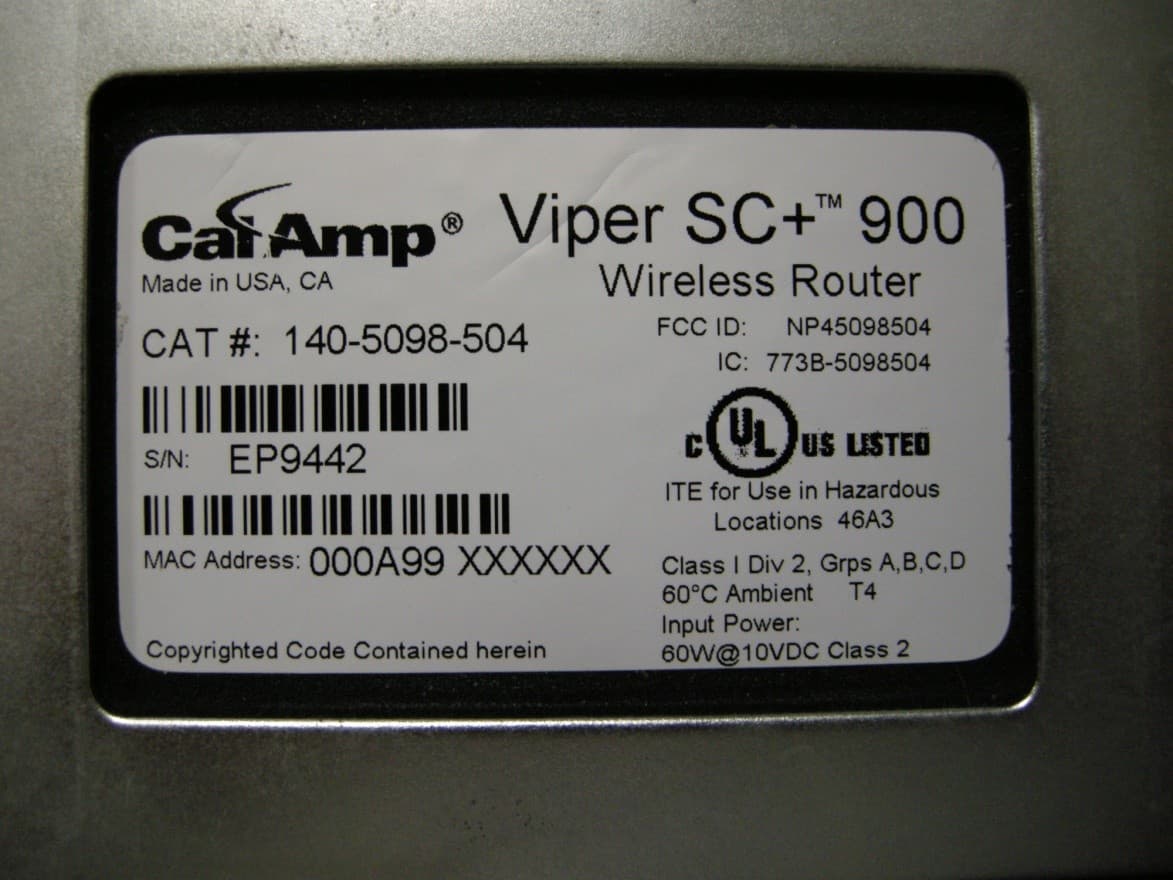
NP45098504
Sep 10, 2013Viper SC+ 928-960 MHz
Equipment Class
PCB - PCS Licensed Transmitter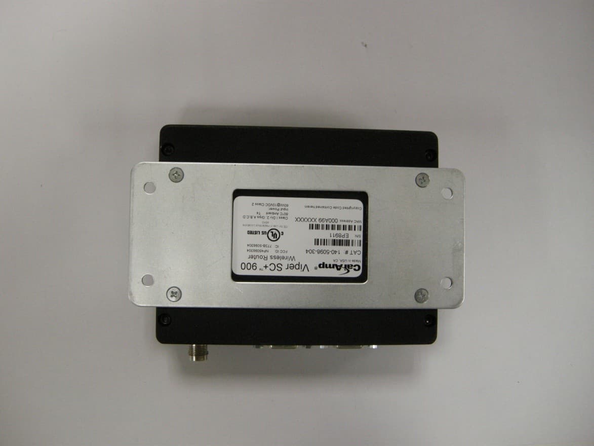
NP45098304
Aug 29, 2013VIPER SC+ 900 VHF 880-902 MHZ
Equipment Class
PCB - PCS Licensed Transmitter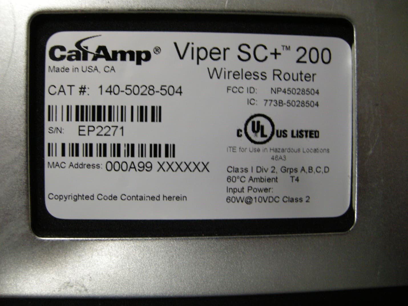
NP45028504
Aug 22, 2013VIPER SC+ 200 VHF 215-240MHZ
Equipment Class
TNB - Licensed Non-Broadcast Station Transmitter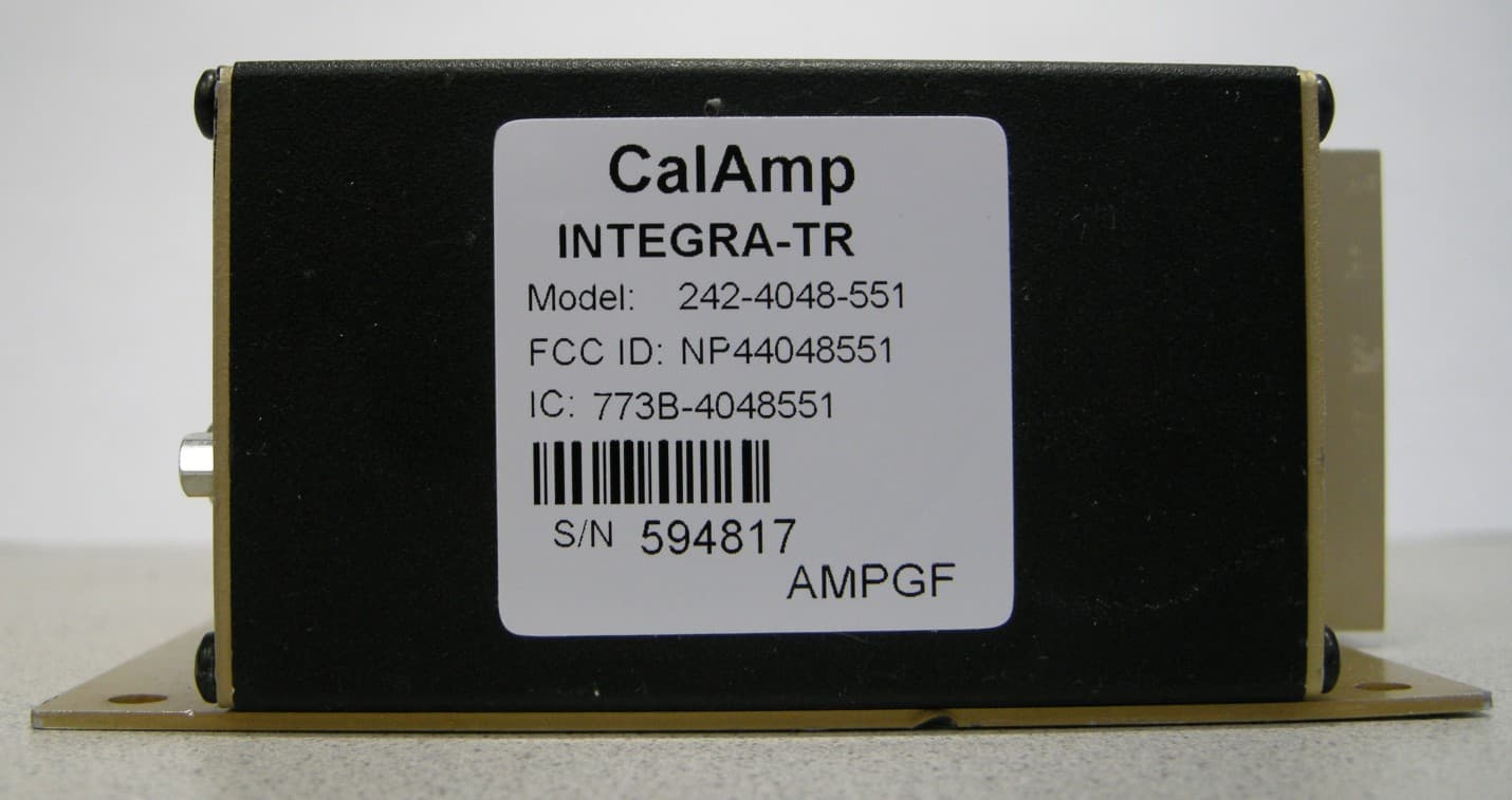
NP44048551
May 09, 2013UHF Wireless Radio Modem
Equipment Class
TNB - Licensed Non-Broadcast Station Transmitter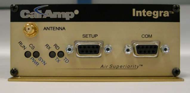
NP44048351
Apr 25, 2013UHF Wireless Radio Modem
Equipment Class
TNB - Licensed Non-Broadcast Station Transmitter