O632225LD02FRS/GMRS
Lionda Technology Co Ltd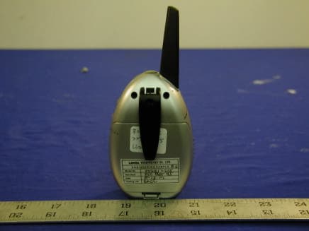
Click to zoom
Application Details
- Equipment Class
- FRF - Part 95 Family Radio Face Held Transmitter
- Date of Grant
- Dec 18, 2002
- Application Purpose
- Original Equipment
- Date of Application
- Dec 17, 2002
- Equipment Note
- FRS/GMRS
- Frequency Range
- 462.56000000 - 467.71000000
- Company
- Lionda Technology Co Ltd
- Country
- China
Documents & Files
Document Text
Text extracted from the exhibit documents filed with the FCC. Open a document above to read the original.
Users Manual
3 5 7 Congratulations on your selection of a quality BeliSouth Product. With proper care and adherence to the sel-up and user instructions in this Owner's Manual, this unit will provide you with years of Irouble-free service BeliSouth is committed to providing qua lily products that fit your needs. We would like to have any comments or suggestions you might have on this product You may mail your comments to: 8 8 8 8 8 10 11 11 11 11 11 12 12 12 13 14 14 15 15 15 SPECIAL FEATURES ,. CARE AND SAFETY FCC NOTICE , GETTING STARTED Removing the Bell Clip Installing the 8eltC~p ConMcting tile Adepter AccessoryConnecl~n 8e1lery1~ LCD Screen Turning \118 UMON "'...""""""."".""." TurnWlg tile Un~ OfF Adjusting Speaker Volume Receiving a S,nal Transmtting a Signal OPERATION Changing CHANNElS MONITDR MENUILOCK Button (FUNCTION EDITIHG) Changing IIhe CTCSS SUa.CHAHNELS VOXSeilcllon ,.. CHANNEL SCAN Blllery ChIIg8 Le¥8k\.ow 8*'Y Indic8Ion To Chatvethe FRSIGMRS Sending CIII TOI* , 16 18 19 22 SPECIFICATIONS TROUBLESHOOTING WARRANTY"" LICENSING " US Electronics 105 Madison Avenue New York, NY 10016 PRODUCT DESCRIPTION The FRS/GMRS COMMUNICATOR is - ~ in peISOI'I8l two-way ccwnmunk:8lklna. The FRS/GMRS CO.uJNK:ATOR _188 in a M:8n-.fr8e r8Iio bend on FRS dWIn8 8 -14 (no FCC li:an&e is naeded tor its oparaIion), 81d on d FRS/GMRS dIaMeIa 1 .7, -' ~ dIann* 15 - 22 ( - pege 22 ~ k8I8Ig ifQmaIk)n) Tha FR~RS is a Iigh'-iglll. ccwnpaa two-way ~tion de.a .., be uaad .. ccwn-1Wc* with I8IIIy or friands aI ~. ~ mala, ~ -. ~ . 8Iy ~ or .,...,... ~ The FRSlGMRS is compatible wIUI oItIer bt8nds utiiziflg the frequency bend (operating in tile fraquency rang- from 482.5625MHz .. 487.7125 MhZ). The FRS/GMRS has 22-CHANNELS, feetulklg - _IIi-functional LCD Sa-. (whidl di8plwys"" current ch_nneland various s_s icons). or.. - id* 0NK)Ff' VOUAoE CONTRa. 81d BATTERY ~ ~UITRY. ~ reed .. o-.I's - ~ .. get - COlt 01 your FRS ~ ~TOR. NOTe: ,.. ~i " ~Inl.. -,.. 00/// ""}' *,.NI.. .. -- oW t ~- wIll N I. 01'"" jWw.. "*1/#,...,. is w _.j I.I/Ji.,.", Is'Z' ,-,.,., TI* ri nI8Y not ensure rwt-;y 01 ~. 2 ~ f~t E.T Q.I'(\.OCATED (Jj TIE fEAR) (1'9.8) BELT CLIP ANTENNA LCD (liquid Crystal Display) Screen - Displays current channej selection and other radio stalus symbols POWER @ button - Press and hold tIll POWER button to turn yourunitON/OFF ~ /lOCK button. Press to shM iIIo FUNCOON EDITING mcxIe Press and h~ for 5 ~s to LOCK'" butkMIS ~ button - Used to activate/deactivate CHANNEL SCAN ~ button. Press 10 transmit CALL Tones TX (Transmission) LED indicator -Illuminates red when Il1nsmilling SPEAKER EAR/MIC/CHARGER JACK. When the earphone is connecied inlo this jack the voice of Ihe speaker will shifllo the earphone. MONITOR 00 button - Press k) wne II and ~ cwm week ~. PUSH TO TALK @ button - Press to transmit. UP Ci) IDOWN C!) buttons - Press to change channels and select FUNCTION in FUNCTION EDITING mode. MIC -MICROPHONE BATTERY COMPARTMENT -Housesw(4)'AAA' eIA.ineorNl-MH rechargeable batteries (batteries not included) M~~ (Ux:ATB> ~ 1tE REAR) (PII. 4. 8. t) 3 Carl and s.flt~ To clean the unit, wipe with e lOft ciolh dampened willi w8l8r. Don't UM cleaners or ool.ents on Ihe unil; they can hum ~ ca.e end iNk iMide, causing permanent damage, eal18ry con18cts ",y be wiped willi a dry, IInI- free ciaI/!. If the unit gets wel, lurn il OFF end remove ~ batlefiH immadi8lely. Dry ,... BATTERY COMPARTMENT wilh a 80ft cIoIIlo minimize poI8ft1i81 weier damage. Laa.. COYer off ~ BATTERY COMPARTMENT oyernigill Of until COrnp1818ly dry Do not... ~ u..1 unlll compl8t8jy dry. E.,..urelo Redlo FreqvertCy Energy The de.~ 01 your FRS/GMRS, which gen- radio frequency (RF)-.- magnetic energy (EME), complies with the ~ natiOll8l8nd in ional s"ndards end guidelin.. Tht Rel..ant Gul4ellnee and 'lan." Are: . FCC Reporlend Order FCC 96-328 (Augusl, 1996) . American Netiona' Slanderdslnstilule (CtS-I-I982) . Natione' CouncW Radielion Prolaclion and Ueasurem..ts (NCRP-1966) .In.m8tklna1 CommiIIion on Non-4onRing Radi8IkIn PIoI8cticII (1CNIRP.I896) TO eneure optimel unit performance end 10 eneure that e._ure to RF energy Is within the guide""es in the above elanderds. the 101l0wlog opere'ing procedures should be ob.e.." For ~ r-. FRM8I . WI-.. ~ ... . F~RS. 1"*1 lie FRSAOMRS ~ . W8tI:8 poI8IxI'" b MK:R~ 1 -. 2 idIM (2.5 -. 5.0 an) ~ ,... ~ K8P .. ANTENNA 81 ~ 2 iIdI (5 an)"""" ~ and body. . If you _r . FRS/GMRS on your body, lilt lie ANTENNA it all.-l Iwo iICh (5 cm) 6om your body - -~. E' ac :.* : Nearty ~ ~ d8YioI. '.-p1b18 kI ~... ~ (all) i ~ 1hiIkIed, d88ign8d. Of oII8rw-. ~ kif ;8fo¥.,.", ~ . T um yoo. unM OFF .. any ~ -'- POII8d -1.-ucI you k) do~. ~ Of - C8f8 ~ mey be ~ 118111 -- kI utemalRF-sJ . T... yoo. uni OFF - on b'*II an ~ ~ kI do~. Any- 0I1he 1111 be .. --- ... -- Of aw i'*Ia-. A CAUTION D dANTENNA I» - - .., ~ ... ... . d8IIIg8d ~ . . ~ AN19IM - iI- .. ... ... . "*I« bIIn ..."", Batt.rIea AI b8I8ri8I ceo ceu.. properly d.m8g8 .nd/Of bodiy qury - .. bumll ~ _I such.. jewelry, keys, Of b88d8d.N ~ PPOl8d The Ift8t8ri8I ...y comp"" .0 1teclrie81~. (1IIaIt dfcuI) 8Id ~ quMe hot, e- cere io 118ndlilU "y dI8II8d ~, ~ pled.. . insid. . pocket. pu..., Of ollie, COftt8Ifter - -, ~. ... WARNING For V.hlcl.. with .n Air e.. I» - ~ jOIK FR~WRS II .,. .roe 0YIr 1ft .. beg Of " tho .. beg ~ _. M b8g1..a. d1 gf88IlOIte. If. FR~ . pIoC8d " 0- ar beg ~.roe 800"" beg ~. lie FR~ mey be ~ ... ...,. 81M! COUll I~ k> lie ~ d .,. vella Pot.nU.lly Explosive Atmosph.r.. Twn~~~F_"..,_MI1'~~~, . . . IW'8 ~ ~ tK IUdI ... (b F-*Iy III*-' ~SI8b" 1UdI- ~ ~"~Of"~" ~a -~ B.tt.ri.s I» -181'18» Of d.-VI be- 10 a ~gy axpiolNe 81ftX1O11h1l8 ConIIct .-ou mey ~ whio -818 Of -"8 -- 800 CO'" 8ft ..~ BI.sUn. Ceps .nd Ar..s To ~ ~ "*"-a .. ~ - jOIK FRSKJMRS OFF - ~ ~ cepe Of i1 . ~ -" « .. 1OIoI8d: "Twn ~ '-.ey -" Q)ey 8If ~ and - NOTE: A wilt poI""'!" ,xploxi., .""'pI."'" ... of ",. bo, .., ./w'.., C'-l, ...It.. r..." i,.,luJ. f.,li,S .re.. x..,. ox b,lo.. uck.. boatx: f..lo.. iN/"US/".,.…
Text truncated - open the document above for the full version.
Block Diagram
2225BD.sch-1 - Wed Nov 06 08:50:50 2002
Cover Letter(s)
Block 2 Laodong 2 nd Industrial Area, Xixian, Baoan, Shenzhen, China Tel.: +86-755-7917824 Fax: +86-755-7917944 November 6, 2002 Federal Communications Commission 7435 Oakland Mills Road Columbia, Maryland, 21046 Sir/Madam, Reg: FCC grand for 2225 (FCC ID. O632225LD02) This letter is an authorization to accept Bay Area Compliance Lab. Corporation as an agent for Lionda Technology Company Limited located at Block 2 Laodong 2 nd Industrial Area, Xixian, Baoan, Shenzhen, China, to sign applications before the Commission on our behalf, to make representations to you on our behalf, and to receive and exchange data between our company and the commission in connection with certification of the following Lionda Technology Company Limited product. This device transmits in both the FRS (Family Radio Service) and GMRS (General Mobile Radio Service) 22 Channel 2-Way Radio With CTCSS security. ERP = 0.5W. Model: 2225 Pursuant to Part 95, FCC rules and regulations. Sincerely, Signature : Printed Name : Dan Coronia Title : Senior Engineer
External Photos
EUT EXTERNAL PHOTOGRAPHS Chassis - Front View Chassis – Rear View Chassis - Top View Chassis – Left Side View Chassis – Right Side View
ID Label/Location Info
APPENDIX A - FCC ID LABELING AND LOCATION Proposed FCC ID Labeling Proposed FCC ID Location Rear Side of EUT / Proposed Label Location FCC ID: O632225LD02 FCC ID: O632225LD02
Internal Photos
EUT INTERNAL PHOTOGRAPHS EUT - Component View EUT – Component View with Antenna EUT - Solder View EUT – Solder View with Antenna
Operational Description
LIONDA TECHNOLOGY COMPANY LIMITED Lionda Research and Development Center 2225seriesdesc Page 1 11/21/02 CIRCUIT DESCRIPTION Model: 2225/2215 a. Receiver Section Radio Frequency signal received by the antenna (ANT1), passing through the Low Pass Filter (L2-L3, C30-C31). The RF signal is then amplified by Low Noise Amplifier Q2 and passes through a Band Pass Filter FL1 (465MHz). The filtered signal within the range of 462 MHz – 467 MHz is then mixed with the first local oscillator signal from the Voltage Controlled Oscillator (VCO) circuit (Q19-Q21, D8, L17) through Q11, a portion of VCO signal is then feedback to the PLL IC (IC5) for phase comparison generating a stable RX Frequency, the output signal is filtered by FL2 (21.7 MHz) which is the first Intermediate Frequency (IF) and is then amplified by Q14. The IF signal is fed to the discriminator IC (IC2) pin 16 which is then mixed with the second local oscillator supplied by crystal X2 (21.25 MHz) to produced and reduced second IF signal. Demodulated signal is recovered through correct adjustment of IF coil (L13) and the internal discriminator circuit of IC2. The recovered Audio signal is outputted at pin 9 of IC2 and then processed through filtering done by U3-D circuit, the fully recovered audio signal is then further amplified by Power Amplifier U3-A. An audible sound is therefore produce by the speaker SPK1, which can be varied from minimum to maximum through the key function (up/down) and process by the CPU IC6. b. Transmitter Section PTT switch when pushed triggers the Transmitter Circuit “ON”, the voice signal generates by the surrounding noise passes through the Microphone MIC1 where mechanical to electrical transformation occurs, the electrical transformed signal is then filtered by a Band Pass Filter U3-A, D, and C. The output signal is Modulated by a modulator circuit with a varactor diode D8 and L17. The external components from Q19-Q21 form a VCO Circuit, which generates the required oscillating frequency for transmission; a portion of this signal is feedback to the PLL IC5 pin 14 for phase comparison in order to produce a stabilized TX frequency. The modulated signal is then amplified by a Cascaded Amplifier Circuit Q17 and Q18 and again amplified by Q24 to produce a sufficient Radio Frequency signal emitted by the Antenna (ANT1). c. Call Transmission By pushing the CALL key, a signal is detected by the CPU (IC6), a CALL data is then produced by the CPU. This data passes through the Band Pass Filter U1-C and modulated by the varactor diode D2 and L8. The signal follows it’s conventional transmission section path through the antenna. d. Continuous Tone Coded Squelch Signal Protocol Once the unit is set to the corresponding Channel and CTCSS code at TX mode a tone is continuously generated from CPU through R96 and R103 and then passes through U1C for filtering and amplification. Then the Coded Tone signal follows its conventional transmission section path. During receiving mode once the Coded Tone signal matched with the set Code the CPU acknowledges and RX mute will disabled and RX will be active. LIONDA TECHNOLOGY COMPANY LIMITED Lionda Research and Development Center 2225seriesdesc Page 2 11/21/02 e. Battery Low Detection Battery Low Detection is controlled by the IC6 as detected on the LCD1, however a voltage divider circuit R50 and R51 serve as the stabilize reference voltage for the IC6 to process its detection. f. Squelch Detection Supported by the linear IC circuit (IC2), a variable resistor VR1 sets the level of detection and Diode D11 acts as a comparator circuit interface with the CPU IC6. g. Power Supply Supply voltage of 6 Volts dc is needed to power “ON” the whole circuitry, by four (4) batteries “AAA” size. LIONDA TECHNOLOGY COMPANY LIMITED Lionda Research and Development Center 2225seriesdesc Page 3 11/21/02 FREQUENCY CHART CHANNEL DISPLAY CHANNEL TYPE FREQ (MHz) POWER (Watts) CHANNEL DISPLAY CHANNEL TYPE FREQ (MHz) POWER (Watts) 1 GMRS/FRS 462.5625 213.8mW 12 FRS 467.6625 162.18mW 2 GMRS/FRS 462.5875 213.8mW 13 FRS 467.6875 162.18mW 3 GMRS/FRS 462.6125 213.8mW 14 FRS 467.7125 162.18mW 4 GMRS/FRS 462.6375 213.8mW 15 GMRS 462.5750 213.8mW 5 GMRS/FRS 462.6625 213.8mW 16 GMRS 462.6250 213.8mW 6 GMRS/FRS 462.6875 213.8mW 17 GMRS 462.6750 213.8mW 7 GMRS/FRS 462.7125 213.8mW 18 GMRS 462.5500 213.8mW 8 FRS 467.5625 162.18mW 19 GMRS 462.6000 213.8mW 9 FRS 467.5875 162.18mW 20 GMRS 462.6500 213.8mW 10 FRS 467.6125 162.18mW 21 GMRS 462.7000 213.8mW 11 FRS 467.6375 162.18mW 22 GMRS 462.7250 213.8mW CTCSS CODE FREQUENCY CHART CODE FREQUENCY (Hz) CODE FREQUENCY (Hz) 1 67.0 20 131.8 2 71.9 21 136.5 3 74.4 22 141.3 4 77.0 23 146.2 5 79.7 24 151.4 6 82.5 25 156.7 7 85.4 26 162.2 8 88.5 27 167.9 9 91.5 28 173.8 10 94.8 29 179.9 11 97.4 30 186.2 12 100.0 31 192.8 13 103.5 32 203.5 14 107.2 33 210.7 15 110.9 34 218.1 16 114.8 35 225.7 17 118.8 36 233.6 18 123.0 37 241.8 19 127.3 38 250.3
Parts List/Tune Up Info
TUNE-UP PROCEDURE Model2225 Page 1 12/6/02 2225 1. TRANSMITTING 1.1 TX VCO ADJUSTMENT a) Connect the DC voltmeter to the test point 1 (TP1). b) Press the PTT Button. c) Adjust L18. d) Specification: 0.9Vdc +/- 0.3 V @ CH 1 1.2 FREQUENCY ADJUSTMENT a) Connect the frequency counter to ANT point. b) Adjust CV1. c) Specification: Tx Frequency +/- 200Hz 1.3 TX POWER CHECK a) Connect the RF level meter to the ANT point (RF impedance: 50Ω) b) Press the PTT button. c) Check the TX Power d) Specification: FRS: < 0.5W GMRS: < 1 W 1.4 MAX. DEVIATION ADJUSTMENT a) Connect the deviation meter to the ANT point. b) Apply the audio signal 1KHz, 4mVrms to the test point 7 (TP7 - MIC input) c) Observe the clipped signal on the scope. d) Adjust SVR1. e) Specification: 2.5KHz Dev +/- 0.15KHz 1.5 MODULATION SENSITIVITY ADJUSTMENT a) Connect the deviation meter to the ANT point. b) Apply the audio signal 1KHz, 8mVrms to the test point (TP7 - MIC input). c) Adjust SVR1. d) Specification: 0.9-1.0KHz Dev 1.6 CALL DATA MODULATION SENSITIVITY CHECK a) Press the Call Button and observe the deviation meter to check the deviation. b) Specification: 1.8KHz +/- 0.5KHz 2. RECEIVING 2.1 RX VCO CHECK a) Connect the DC voltmeter to test point 1 (TP1). b) Check the DC voltage. c) Specification: 0.9Vdc +/- 0.6V @ CH 1 TUNE-UP PROCEDURE Model2225 Page 2 12/6/02 2225 2.2 QUAD COIL ADJUSTMENT a) Connect the DC voltmeter to the test point 3 (TP3). b) Adjust the IFT1. c) Specification: 1.5Vdc +/- 0.2V 2.3 SENSITIVITY CHECK a) Connect the Sinnader meter to test point 5 (TP5). b) Reduce the RF output level of signal generator to get the 12dB of Sinnader. c) Specification: <-116dBm 2.4 SQUELCH THRESHOLD POINT ADJUSTMENT a) Connect the DC voltmeter to test point 16. b) Same setup as the Sensitivity Check. c) Adjust the SVR1 to get the DC changing point. d) Specification: 7dB +/- 1dB 2.5 SPEAKER OUTPUT LEVEL CHECK a) Connect the Audio level meter to test point 5 (TP5). b) Connect the 8Ω load to test point 5 (TP5). c) Press the volume button till its maximum level. d) Adjust the modulation deviation of RF signal generator. e) Check the clipping start deviation & level. f) Specification: Clipping start deviation = >0.6KHz Level = -2 +/- 4 dBm NOTE: 1. Press PTT button continuously when checking TRANSMITTING parameters. 2. Press the Monitor button to disable the RX power saving when the RX is not stable. 3. OTHER PARAMETER CHECKING 3.1 LOW BATTERY DETECT VOLTAGE CHECK a) Change the voltage until the Battery icon is flashing on the LCD. b) Check the voltage. c) Specification: 4.2Vdc +/- 0.3V
Schematics
2225.sch-2 - Wed Nov 06 08:49:47 2002
Schematics
2225.sch-1 - Wed Nov 06 08:48:17 2002
Test Report
Note: This test report is specially limited to the above client company and product model. It may not be duplicated without prior written consent of Bay Area Compliance Laboratory Corporation. This report must not be used by the client to claim product endorsement by NVLAP or any agency of the U.S. Government. . FCC PART 95 EMI MEASUREMENT AND TEST REPORT For Lionda Technology Company Limited Block 2 Laodong 2 nd Industrial Area, Xixian, Baoan, Shenzhen, Guangdong, China 518102 FCC ID: O632225LD02 December 5, 2002 This Report Concerns: Original Report Equipment Type: FRS & GMRS Test Engineer: Jeff Lee Report Number: R0210252 Test Date: November 13, 2002 Reviewed By: Hans Mellberg Prepared By: Bay Area Compliance Laboratory Corporation 230 Commercial Street Sunnyvale, CA 94085 Tel: (408) 732-9162 Fax: (408) 732 9164 Lionda Technology Co. Ltd. FCC ID: O632225LD02 Report # R0210252Rpt.doc FCC Part 95 Test Report Page 2 of 23 TABLE OF CONTENTS 1 - GENERAL INFORMATION.................................................................................................................................................4 1.1 PRODUCT DESCRIPTION FOR EQUIPMENT UNDER TEST (EUT)........................................................................................4 1.2 OBJECTIVE................................................................................................................................................................................4 1.3 RELATED GRANT/SUBMISSION..............................................................................................................................................4 1.4 TEST METHODOLOGY..............................................................................................................................................................4 1.5 TEST FACILITY.........................................................................................................................................................................5 1.6 TEST EQUIPMENT LIST............................................................................................................................................................5 2 - SYSTEM TEST CONFIGURATION..................................................................................................................................6 2.1 JUSTIFICATION..........................................................................................................................................................................6 2.2 EUT TEST CONFIGURATION..................................................................................................................................................6 2.3 SPECIAL ACCESSORIES............................................................................................................................................................6 2.4 SCHEMATICS / BLOCK DIAGRAM...........................................................................................................................................6 2.5 EQUIPMENT MODIFICATIONS.................................................................................................................................................6 2.6 CONFIGURATION OF TEST SYSTEM.......................................................................................................................................7 2.7 TEST SETUP BLOCK DIAGRAM...............................................................................................................................................7 3 - REQUIREMENTS OF PROVISIONS................................................................................................................................8 3.1 REQUIREMENTS AND TEST SUMMARY..................................................................................................................................8 3.2 LABELING REQUIREMENT.......................................................................................................................................................8 4 - EFFECTIVE RADIATED POWER.....................................................................................................................................9 4.1 PROVISION APPLICABLE.........................................................................................................................................................9 4.2 TEST PROCEDURE....................................................................................................................................................................9 4.3 TEST EQUIPMENT....................................................................................................................................................................10 4.4 TEST RESULTS........................................................................................................................................................................10 5 - MODULATION CHARACTERISTICS...........................................................................................................................11 5.1 PROVISION APPLICABLE.......................................................................................................................................................11 5.2 TEST PROCEDURE..................................................................................................................................................................11 5.3 TEST EQUIPMENT...................................................................................................................................................................11 5.4 TEST RESULTS........................................................................................................................................................................11 6 - OCCUPIED BANDWIDTH OF EMISSION..........................................................................................................…
Text truncated - open the document above for the full version.
Test Setup Photos
APPENDIX B - TEST SETUP PHOTOGRAPHS Radiated Emission - Front View Radiated Emission - Rear View
Contact Information
Applicant
Dan Coronia(Senior Engineer)
Test Firm
Bay Area Compliance LaboratoryJohn Chan
Technical Specifications
| # | Rule Parts | Frequency Range | Power Output | Emission | Tolerance |
|---|---|---|---|---|---|
| 2 | 95B | 462.56 MHz - 467.71 MHz | 162.18 mW | 11K0F3E | 2.5 ppm |
Other Applications from Lionda Technology Co Ltd
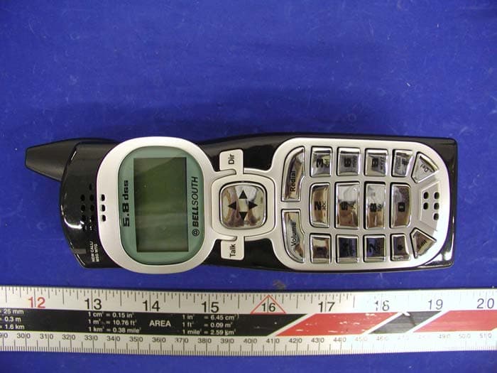
O63GH5850HDLD03
May 23, 2004Digital Cordless Phone � Handset Unit
Equipment Class
DTS - Digital Transmission System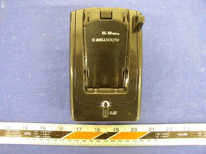
O63GH5815BALD04
Apr 15, 2004Analog Cordless Phone
Equipment Class
DXX - Part 15 Low Power Communication Device Transmitter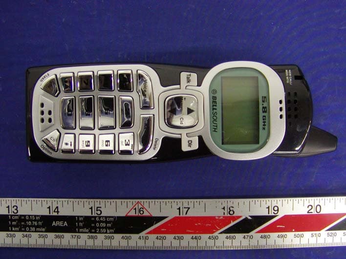
O63GH5815HALD04
Apr 15, 2004Analog Cordless Phone
Equipment Class
DXX - Part 15 Low Power Communication Device Transmitter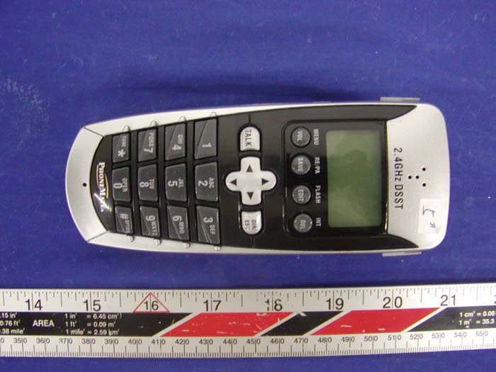
O63PM3320DLD04
Apr 05, 20042.4GHz Digital Spread-Spectrum Cordless Phone
Equipment Class
DTS - Digital Transmission System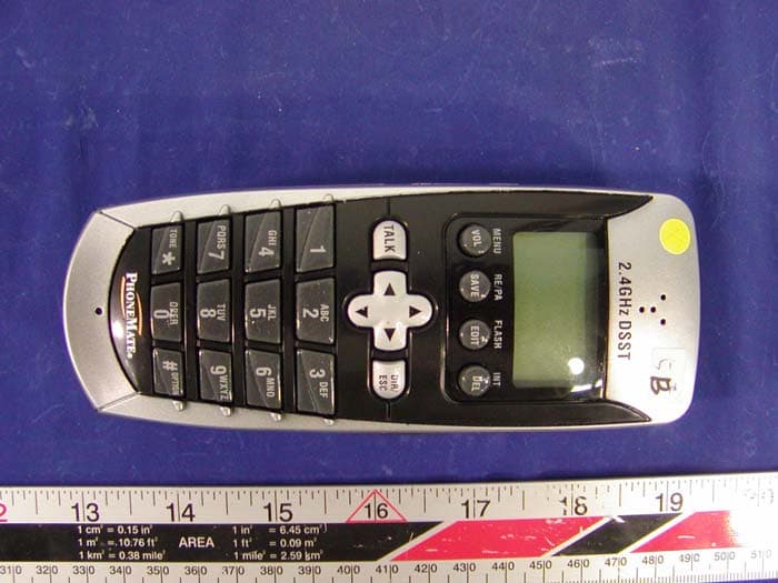
O63PM3375DLD04
Mar 29, 20042.4GHz Digital Spread-Spectrum Cordless Phone
Equipment Class
DTS - Digital Transmission System