O632232LD02FRS / GMRS Transceiver
Lionda Technology Co Ltd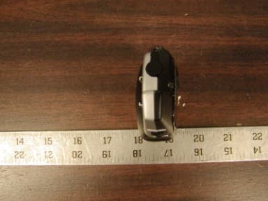
Click to zoom
Application Details
- Equipment Class
- FRF - Part 95 Family Radio Face Held Transmitter
- Date of Grant
- Aug 25, 2002
- Application Purpose
- Original Equipment
- Date of Application
- Aug 25, 2002
- Equipment Note
- FRS / GMRS Transceiver
- Frequency Range
- 462.56000000 - 467.72000000
- Company
- Lionda Technology Co Ltd
- Country
- China
Documents & Files
Document Text
Text extracted from the exhibit documents filed with the FCC. Open a document above to read the original.
Users Manual
2 Changing CHANNELS MONITOR MODE/LOCK Battery Sending Call Tones ..........................................................12 ................................................... ...................... 12 ............................. 12 .............................................................15 Button (FUNCTION EDITING) TRANSMIT POWER SELECTION Mode CHANNEL SCAN Charge Level/Low Battery Indication To Charge the FRS/GMRS ................................... 13 ................................................................. 14 .............................. 14 ...................................................... 15 SPECIFICATIONS CHANNEL TABLE ...................................................................15 .................................................................... 16 .......................................................................21 TROUBLESHOOTING WARRANTY LICENSING .............................................................. 17 ............................................................................18 ..... Removing the Belt Clip Installing the Belt Clip Connecting the Adapter Accessory Connection ........................................................8 .........................................................8 ......................................................8 ........................................................8 Battery Installation LCD Screen Turning the Unit ON Turning the Unit OFF Adjusting Speaker Volume Receiving a Signal Transmitting a Signal .............................................................9 .................................................................... 10 ............................................................ 11 .......................................................... 11 .................................................... 11 ........................................................... 11 .......................................................... 11 OPERATION SPECIAL FEATURES CARE AND SAFETY FCC NOTICE ...................................................3 .....................................................5 ...............................................................7 GETTING STARTED Contents 4 Special FeaturesSpecial Features 1 around buildings or large structures. NOTE:The maximum transmission range will vary depending on terrain and environment. Range will be greater in open fields, while range is shorter within and PRODUCT DESCRIPTION The FRS/GMRS COMMUNICATOR is the newest generation in personal two-way communications. The FRS/GRMS COMMUNICATOR operates in a licensed-free radio band on the FRS channels 8 -14 (no FCC license is needed for its operation), and on licensed FRS/GMRS channels 1 - 7, and GMRS channels 15 - 22 ( see page 22 regarding licensing information). The FRS/GMRS is a lightweight, compact two-way communication device that can be used to communicate with family or friends at parks, shopping malls, sporting events, concerts - any indoor or outdoor activity! The FRS/GMRS is compatible with other brands utilizing the same frequency band (operating in the frequency range from 462.5625MHz The FRS/GMRS has 22-CHANNELS, featuring a multi-functional LCD Screen (which displays the current channel and various status icons). This unit may not ensure privacy of communication. Please read this Owner's Manual carefully to get the most out of your FRS/ GMRS.COMMUNICATOR BellSouthis committed to providing quality products that fit your needs. We would like to have any comments or suggestions you might have on this product. You may mail U.S. Electronics 105 Madison Avenue New York, NY 10016 your comments to: you with years of trouble-free service. to 462.7250 MHz). Congratulations on your selection of a quality . With proper care and adherence to the set-up and user instructions in this Owner's Manual, this unit will provide BellSouth Product BELT CLIP MONITOR button- Press to tune in and hold onto weak signals. UP / DN (DOWN) buttons- Used for changing channels, codes, and setting the receive volume. TALK (PUSH TO TALK) button- Used for making a call. CALL button- Press to transmit a CALL Tones. MIC - Microphone ANTENNA LCD (Liquid Crystal Display) Screen- Displays current channel selection and other radio status symbols. BATTERY COMPARTMENT COVER LATCH(Located on the rear) - Secures BATTERY COMPARTMENT cover. EAR/MIC jack- This jack is used to connect a 3.5 mm stereo headset/mic. POWER ON/OFF buttonPOWER- Press and hold thebutton to turn the unit ON or OFF. MODE /LOCK button- Press to shift into FUNCTION editing mode. Press and hold for 5 seconds to lock the buttons. SPEAKER BATTERY COMPARTMENT- Houses four(4)alkaline or Ni-MH rechargeable batteries (not (Located on the rear) included with the package). SCAN button- Used to activate and deactivate channel scanning. TX LED indicator- Illuminates red when transmitting. CALL BELT CLIP(LOCATED ON THE REAR) (Pg. 8) EAR/MIC/CHARGER JACK (Pgs. 8, 14) ANTENNA (Pgs. 5-7) UP BUTTON (VOLUME/CHANNEL) (Pgs. 4, 11-14, 17) DOWN BUTTON (VOLUME/CHANNEL) (Pgs. 4, 11-14, 17) BATTERY COMPARTMENT (LOCATED INSIDE) (Pgs. 4, 6, 9) TX LED INDICATOR (Pg. 4, 11, 14) CALL BUTTON (Pg. 4, 12, 14) SCAN BUTTON (Pg. 4, 13, 14) SPEAKER (Pg. 11) LCD SCREEN (Pgs. 4, 10-14, 17) PTT BUTTON (PUSH TO TALK) (Pgs.4, 7, 11-14) 2252 MODE BUTTON (Pgs. 4, 10, 12, 13, 17) POWER ON/OFF BUTTON (Pgs. 4, 9, 11, 14) MONITOR BUTTON (Pgs. 4, 11, 12, 17) VX SC Figure 1 Figure 2 Getting Started 8 Removing the BELT CLIP Installing the BELT CLIP Connecting the Adapter 1. Pull the BELT CLIP LATCH away from the unit. 2. While pulling the BELT CLIP LATCH, push up on the BELT CLIP to remove it from the unit, as shown in Figure 1. 1. Slide the BELT CLIP into the BELT CLIP SLOT as shown in Figure 2. package.) Care and SafetyCare and Safety NOTE:Areas with potentially explosive atmospheres are often, but not always, clearly marked. They include fueling areas such as below deck on boats; fuel or chemical transfer…
Text truncated - open the document above for the full version.
Cover Letter(s)
Block 2 Laodong 2 nd Industrial Area, Xixian, Baoan, Shenzhen, China Tel.: +86-755-7917824 Fax: +86-755-7917944 August 09, 2002 Federal Communications Commission 7435 Oakland Mills Road Columbia, Maryland, 21046 Sir/Madam, Reg: FCC grand for 2252/2232 (FCC ID. O632232LD02) This letter is an authorization to accept Bay Area Compliance Lab. Corporation as an agent for Lionda Technology Company Limited located at Block 2 Laodong 2 nd Industrial Area, Xixian, Baoan, Shenzhen, China, to sign applications before the Commission on our behalf, to make representations to you on our behalf, and to receive and exchange data between our company and the commission in connection with certification of the following Lionda Technology Company Limited product. This device transmits in both the FRS (Family Radio Service) and GMRS (General Mobile Radio Service) 22 Channel 2-Way Radio With CTCSS security. ERP = 0.104W. Model: 2252/2232 Pursuant to Part 95, FCC rules and regulations. Sincerely, Signature: Printed Name :Dan Coronia Title:Senior Engineer
Cover Letter(s)
American Telecommunications Certification Body Inc. 6731 Whittier Ave, McLean, VA 22101 August 18, 2002 RE: FCC ID: O632232LDO2 Attention: John Chan / Jennifer Song I have a few comments on this Application. 1 Section 5.2.2 of the report says that you set The audio signal generator frequency was set between 1000 MHz and the upper low pass filter limit. Please correct the report to state the proper frequencies. xx 2 Your frequency stability data states ppm and %. Please select one or the other as a deviation reference and please correct the appropriate data to show this selection. Please note that since both FRS and GMRS specify tolerance in %, this would probably be the best reference to use for frequency stability. 3 Section 7 of your reports states that Radiated Spurious emissions data passed. Please note that a designation of low, middle and high is not sufficient for showing compliance. Please specify what these frequencies are and please provide objective evidence in plot or tabular data that Radiated Spurious emissions is compliant. xx 4 Section 8 of your report states that Spurious emissions passed, and then it states that plots of the data were attached. Please note no plots of spurious emissions data was contained in the report. Please provide these plots to support your claim of spurious emissions compliance. xx 5 Your 731 says the emissions designator is 10k0F3E while the calculation in the report states, 11k0F3E. Please specify provide corrected documentation as to what the actual emissions designator is. xx 6 You occupied bandwidth plot shows what appears to be an unmodulated signal as well as the modulated signal. The unmodulated signal appears to be 20dBm. This plot also appears to be an antenna conducted plot. This level appears to be the same as that of the EIRP value reported in the report. It is unusual for conducted power and EIRP to be the same. Please explain. 7 While the device appears under the low threshold where SAR would be required, you have provided an RF exposure statement. However, the statement information you have provided is not complete. Please provide complete the information as contained in the manual. Dennis Ward mailto:[email protected] The items indicated above must be submitted before processing can continue on the above referenced application. Failure to provide the requested information may result in application termination. Correspondence should be considered part of the permanent submission and may be viewed from the Internet after a Grant of Equipment Authorization is issued. Please do not respond to this correspondence using the email reply button. In order for your response to be processed expeditiously, you must submit your documents through the AmericanTCB.com website. Also, please note that partial responses increase processing time and should not be submitted. Any questions about the content of this correspondence should be directed to the sender.
Cover Letter(s)
American Telecommunications Certification Body Inc. 6731 Whittier Ave, McLean, VA 22101 August 26, 2002 RE: FCC ID: O632232LDO2 Attention: John Chan / Jennifer Song I have a few comments on this Application. 1Your spurious emissions data is higher than your listed FCC limits. Please note this shows failure, not compliance. Please show the proper limits and the proper derivation of spurious emissions and the FCC limits used. Dennis Ward mailto:[email protected] The items indicated above must be submitted before processing can continue on the above referenced application. Failure to provide the requested information may result in application termination. Correspondence should be considered part of the permanent submission and may be viewed from the Internet after a Grant of Equipment Authorization is issued. Please do not respond to this correspondence using the email reply button. In order for your response to be processed expeditiously, you must submit your documents through the AmericanTCB.com website. Also, please note that partial responses increase processing time and should not be submitted. Any questions about the content of this correspondence should be directed to the sender.
Cover Letter(s)
Subject: Re: request for information on O632232LD02 Date: Fri, 23 Aug 2002 16:09:26 -0700 From: "Jennifer Song" <[email protected]> Organization: BACL To: <[email protected]>, "dennis" <[email protected]>, "William Graff" <[email protected]> CC: "Pin Wen" <[email protected]> Hi, Dennis and Bill, I have just updated our test report for O632232LD02 to your website, with the file "new test report2.pdf". Please check it out. According to your request, we changed following places in the report: 1. Page 8: Sec.3.1 2. Page 10: Sec.4.4 3. Page 16: Sec.7.2 and Sec.7.4 Thank you! Best Regards, Jennifer Song BACL, Documentation Personnel Email: [email protected] Tel: 408-732-9162 * 39 Fax: 408-732-9164
External Photos
Shenzhen Bao An Hantong Electronics Factory FCC ID: O632232LD02 Report # R0207088FCC Part 95 Test Report EUT External Photographs EUT - Top View EUT - Front View Shenzhen Bao An Hantong Electronics Factory FCC ID: O632232LD02 Report # R0207088FCC Part 95 Test Report EUT - Rear View EUT – Port Side View
ID Label/Location Info
Shenzhen Bao An Hantong Electronics Factory FCC ID: O632232LD02 Report # R0207088FCC Part 95 Test Report FCC ID Labeling and Location Proposed FCC ID Labeling Proposed FCC ID Location Rear Side of EUT FCC ID: O632232LD02 Proposed FCC ID Location label here
Internal Photos
Shenzhen Bao An Hantong Electronics Factory FCC ID: O632232LD02 Report # R0207088FCC Part 95 Test Report EUT Internal Photographs EUT – Component View EUT – Component Cover off View Shenzhen Bao An Hantong Electronics Factory FCC ID: O632232LD02 Report # R0207088FCC Part 95 Test Report EUT – Solder View EUT – Antenna View
Operational Description
LIONDA TECHNOLOGY COMPANY LIMITED Lionda Research and Development Center 2252seriesdescPage 18/27/02 CIRCUIT DESCRIPTION Model: FRS/GMRS 2252 (0.5watt~1watt) a. Receiver Section Radio Frequency signal received by the antenna (ANT1), passing through the Low Pass Filter (L2-L3, C30-C31). The RF signal is then amplified by Low Noise Amplifier Q2 and passes through a Band Pass Filter FL1 (465MHz). The filtered signal within the range of 462 MHz – 467 MHz is then mixed with the first local oscillator signal from the Voltage Controlled Oscillator (VCO) circuit (Q19-Q21, D5, L17) through Q11, a portion of VCO signal is then feedback to the PLL IC (IC5) for phase comparison generating a stable RX Frequency, the output signal is filtered by FL2 (21.7 MHz) which is the first Intermediate Frequency (IF) and is then amplified by Q14. The IF signal is fed to the discriminator IC (IC2) pin 16 which is then mixed with the second local oscillator supplied by crystal X2 (21.65 MHz) to produced and reduced second IF signal. Demodulated signal is recovered through correct adjustment of IF coil (L13) and the internal discriminator circuit of IC2. The recovered Audio signal is outputted at pin 9 of IC2 and then processed through filtering done by U3-D circuit, the fully recovered audio signal is then further amplified by Power Amplifier U3-A. An audible sound is therefore produce by the speaker SPK1, which can be varied from minimum to maximum through the key function (up/down) and process by the CPU IC6. b. Transmitter Section PTT switch when pushed triggers the Transmitter Circuit “ON”, the voice signal generates by the surrounding noise passes through the Microphone MIC1 where mechanical to electrical transformation occurs, the electrical transformed signal is then filtered by a Band Pass Filter U3-A, D, and C. The output signal is Modulated by a modulator circuit with a varactor diode D8 and L17. The external components from Q19-Q21 form a VCO Circuit, which generates the required oscillating frequency for transmission; a portion of this signal is feedback to the PLL IC5 pin 14 for phase comparison in order to produce a stabilized TX frequency. The modulated signal is then amplified by a Cascaded Amplifier Circuit Q17 and Q18 and again amplified by Q24 to produce a sufficient Radio Frequency signal emitted by the Antenna (ANT1). c. Call Transmission By pushing the CALL key, a signal is detected by the CPU (IC6), a CALL data is then produced by the CPU. This data passes through the Band Pass Filter U1-C and modulated by the varactor diode D2 and L8. The signal follows it’s conventional transmission section path through the antenna. d. Continuous Tone Coded Squelch Signal Protocol Once the unit is set to the corresponding Channel and CTCSS code at TX mode a tone is continuously generated from CPU through R96 and R103 and then passes through U1C for filtering and amplification. Then the Coded Tone signal follows its conventional transmission section path. During receiving mode once the Coded Tone signal matched with the set Code the CPU acknowledges and RX mute will disabled and RX will be active. LIONDA TECHNOLOGY COMPANY LIMITED Lionda Research and Development Center 2252seriesdescPage 28/27/02 e. Battery Low Detection Battery Low Detection is controlled by the IC6 as detected on the LCD1, however a voltage divider circuit R50 and R51 serve as the stabilize reference voltage for the IC6 to process its detection. f. Squelch Detection Supported by the linear IC circuit (IC2), a variable resistor VR1 sets the level of detection and Diode D11 acts as a comparator circuit interface with the CPU IC6. g. Power Supply Supply voltage of 6 Volts dc is needed to power “ON” the whole circuitry, by four (4) batteries “AAA” size. FREQUENCY CHART CHANNEL DISPLAY CHANNEL TYPE FREQ (MHz) POWER (Watts) CHANNEL DISPLAY CHANNEL TYPE FREQ (MHz) POWER (Watts) 1GMRS/FRS 462.56251 12FRS467.66250.5 2GMRS/FRS 462.58751 13FRS467.68750.5 3GMRS/FRS 462.61251 14FRS467.71250.5 4GMRS/FRS 462.6375115GMRS 462.55001 5GMRS/FRS 462.6625116GMRS 462.57501 6GMRS/FRS 462.6875117GMRS 462.60001 7GMRS/FRS 462.7125118GMRS 462.62501 8FRS467.56250.5 19GMRS 462.65001 9FRS467.58750.5 20GMRS 462.67501 10FRS467.61250.5 21GMRS 462.70001 11FRS467.63750.5 22GMRS 462.72501 CTCSS CODE FREQUENCY CHART CODEFREQUENCY (Hz)CODEFREQUENCY (Hz) 167.020131.8 271.921136.5 374.422141.3 477.023146.2 579.724151.4 682.525156.7 785.426162.2 888.527167.9 991.528173.8 1094.829179.9 1197.430186.2 12100.031192.8 13103.532203.5 14107.233210.7 15110.934218.1 16114.835225.7 17118.836233.6 18123.037241.8 19127.338250.3
Parts List/Tune Up Info
slc_npart descrip rev Qty. reference smt 12D-1420-004A CRYSTAL FILTERS 21.3MHz(ft21.3)3dB BANDWIDTH +/-3.75KHz P0 2 FL2,FL3 111-6103-002A IC_MEM 24LC02 (SOIC-8) P0 1 IC3 Y 112-2213-001B TR_RF POWER BFQ540(SOT-89) P0 1 Q16 Y 128-1213-090A CAP_C_CHIP 9PF/D(CH)(0603) A:COG150L P0 1 C154 Y 128-22A9-104A CAP_C_C.H.D. F0.1uF/Z(0603) Y:YF153L P0 30 C1,C4,C5,C13,C16,C22,C25,C26,C36,C41,C44,C51,C54,C69,C81 Y 128-22A9-104A CAP_C_C.H.D. F0.1uF/Z(0603) Y:YF153L P0 0 C64,C65,C71,C78,C80,C86,C96,C99,C106,C125,C126,C135,C150 Y 128-1216-101A CAP_C_CHIP 100PF/J(CH)(0603) A:COG150L P0 4 C28,C107,C127,C130 Y 128-2297-103A CAP_C_C.H.D. B0.01uF/K(0603) X:X7R282L P0 17 C2,C21,C46,C70,C74,C82,C89,C91,C98,C103,C104,C110 Y 128-2297-103A CAP_C_C.H.D. B0.01uF/K(0603) X:X7R282L P0 0 R103,C113,C141,C151,C161 Y 128-1213-100A CAP_C CHIP 10PF/D/(CH)/(0603) A:COG150L P0 4 C48,C49,C84,C143 Y 128-1216-120A CAP_C_CHIP 12PF/J(CH)(0603) A:COG150L P0 2 C31,C114 Y 128-2297-102A CAP_C_C.H.D. B0.001uF/K(0603) X:X7R282L P0 10 C24,C33,C53,C62,C102,C119,C140,C145,C147,C148 Y 128-1211-010A CAP_C CHIP 1PF/B/(CH)/(0603) A:COG150L P0 2 C123,C161 Y 128-23A9-105A CAP_C_C.H.D. F 1uF/Z(0805) Y:YF153L P0 10 C6,C9,C14,C23,C27,C90,C136,C138,C146,C165 Y 128-2297-222A CAP_C_C.H.D. B0.0022uF/K(0603) X:X7R282L P0 1 C12 Y 128-1211-2R2A CAP_C CHIP 2.2PF/B/(CH)/(0603) A:COG150L P0 1 C139 Y 128-1216-200A CAP_C_CHIP 20PF/J(CH)(0603) A:COG150L P0 3 C83,C95,C131 Y 128-23A9-224A CAP_C_C.H.D.F0.22uF/Z(0805) Y:YF153L P0 2 C37,C152 Y 128-1216-221A CAP_C_CHIP 220PF/J(CH)(0603) A:COG150L P0 8 C8,C10,C58,C60,C85,C129,C134,C137 Y 128-2297-223A CAP_C_C.H.D. B0.022uF/K(0603) X:X7R282L P0 9 C45,C47,C50,C52,C55,C61,C63,C68,C105 Y 128-1216-220A CAP_C_CHIP 22PF/J(CH)(0603) A:COG150L P0 1 C117 Y 128-1211-020A CAP_C CHIP 2PF/B(+/-0.15PF)/(CH)/(0603) A:COG150L P0 3 C87,C168,R236 Y 128-1211-3R3A CAP_C CHIP 3.3PF/B/(CH)/(0603) A:COG150L P0 3 C118,C120,C122 Y 128-1216-300A CAP_C_CHIP 30PF/J(CH)(0603) A:COG150L P0 2 C38,C39 Y 128-1216-331A CAP_C_CHIP 330PF/J(CH)(0603) A:COG150L P0 2 C72,C73 Y 128-23A9-474A CAP_C_C.H.D.F0.47uF/Z(0805) Y:YF153L P0 3 C18,C20,C35 Y 128-1216-471A CAP_C_CHIP 470PF/J(CH)(0603) A:COG150L P0 3 C19,C88,C144 Y 128-22A8-473A CAP_C_C.H.D. F0.047uF/M(0603) Y:YF153L P0 5 C40,C66,C75,C76,C79 Y 128-1216-561A CAP_C_CHIP 560PF/J(CH )(0603) A:COG150L P0 3 C3,C7,C43 Y 128-1213-050A CAP_C_CHIP 5PF/D(CH)(0603) A:COG150L P0 3 C30,C93,C124 Y 128-1213-060A CAP_C_CHIP 6PF/D(CH)(0603) A:COG150L P0 2 C109,C155 Y 128-1213-070A CAP_C_CHIP 7PF/D(CH)(0603) A:COG150L P0 2 C115,C158 Y 128-1216-820A CAP_C_CHIP 82PF/J(CH)(0603) A:COG150L P0 2 C128,C133 Y 128-1213-080A CAP_C_CHIP 8PF/D(CH)(0603) A:COG150L P0 2 C92,C121 Y 125-0255-003A CHIP SPRING COIL D1.2X0.32X3T P0 2 L3,L8 Y 125-0122-S12A CHIP COIL SQUARE 12nH/J(0603) P0 3 L5,L10,L12 Y 125-0133-2R2A CHIP COIL SQUARE 2.2uH/K(0805) P0 1 L7 Y 114-1207-001A DIODE_SW LL4148/MM4148 MELF P0 3 D4,D13,D14 Y 114-1109-001A DIODE_SW KDS114(URP) P0 4 D2,D3,D5,R39 Y 125-0255-004A CHIP SPRING COIL D1.2X0.32X4T P0 4 L2,L4,L9,L17 Y 111-2103-008A IC_LI KA386/LM386(SOP) P0 1 IC1 Y 114-4008-001A DIODE_VAR KDV154B(SOT-23) P0 1 D8 Y 111-2103-005A IC_LI KA324/KIA324/LM324(SOP) P0 3 U1,U2,U3 Y 112-1306-001C TR_SS MMBT3904LT1(SOT-23) P0 6 Q3,Q4,Q9,Q15,Q21,Q23 Y 112-2306-001A TR_RF KTC3880Y SOT23 P0 1 Q14 Y 112-2306-003A TR_RF 2SC4901 (SOT-23) HFE:120-250 P0 6 Q2,Q11,Q17,Q18,Q19,Q20 Y 112-1106-001A TR_SS KST2907TF/KTN2907S/AS /MMBT2907LT1(SOT-23) P0 6 Q1,Q5,Q6,Q7,Q12,Q13 Y 122-0224-122A RES_(0603)-10 1.2 KOHM P0 1 R81 Y 122-0224-182A RES_(0603)-10 1.8 KOHM P0 1 R71 Y 122-0224-100A RES_(0603)-10 10 OHM P0 10 R10,R18,R22,R53,R69,R89,R94,R126,R151,R152 Y 122-0224-101A RES_(0603)-10 100 OHM P0 3 R38,R43,R135 Y 122-0224-104A RES_(0603)-10 100 KOHM P0 18 R11,R21,R52,R56,R62,R68,R73,R84,R85,R86,R97,R144 Y 122-0224-104A RES_(0603)-10 100 KOHM P0 0 R61,R204,R205,R231,R232,R233 Y 122-0224-103A RES_(0603)-10 10 KOHM P0 9 R13,R20,R54,R83,R101,R134,R139,R145,R230 Y 122-0224-124A RES_(0603)-10 120 KOHM P0 3 R3,R5,R67 Y 122-0224-154A RES_(0603)-10 150 KOHM P0 2 R58,R66 Y 122-0224-153A RES_(0603)-10 15 KOHM P0 2 R4,R9 Y 122-0224-183A RES_(0603)-10 18 KOHM P0 3 R26,R200,R203 Y 122-0224-222A RES_(0603)-10 2.2 KOHM P0 7 R42,R76,R116,R117,R122,R131,R153 Y 122-0224-272A RES_(0603)-10 2.7 KOHM P0 3 R29,R65,R93 Y 122-0224-224A RES_(0603)-10 220 KOHM P0 10 R209,R210,R211,R212,R213,R214,R215,R216,R217,R218 Y 122-0224-223A RES_(0603)-10 22 KOHM P0 15 R23,R30,R40,R44,R46,R47,R48,R49,R50,R51,R115,R127,R150 Y 122-0224-273A RES_(0603)-10 27 KOHM P0 1 R206 Y 122-0224-392A RES_(0603)-10 3.9 KOHM P0 1 R57 Y 122-0224-330A RES_(0603)-10 33 OHM P0 5 R77,R80,R123,R136,R143 Y 122-0224-331A RES_(0603)-10 330 OHM P0 2 R79,R91 Y 122-0224-334A RES_(0603)-10 330 KOHM P0 3 R1,R95,C178 Y 122-0224-333A RES_(0603)-10 33 KOHM P0 3 R24,R41,R82 Y 122-0224-393A RES_(0603)-10 39 KOHM P0 1 R25 Y 122-0224-4R7A RES_(0603)-10 4.7 OHM P0 1 R15 Y 122-0224-472A RES_(0603)-10 4.7 KOHM P0 11 R33,R34,R35,R45,R92,R114,R120,R121,R124,R125,R148 Y 122-0224-474A RES_(0603)-10 470 KOHM P0 4 R6,R55,R59,R229 Y 122-0224-473A RES_(0603)-10 47 KOHM P0 8 R8,R16,R17,R31,R32,R36,R113,R119 Y 122-0224-562A RES_(0603)-10 5.6 KOHM P0 4 R28,R60,R70,R72 Y 122-0224-513A RES_(0603)-10 51 KOHM P0 1 R207 Y 122-0224-560A RES_(0603)-10 56 OHM P0 2 R129,R146 Y 122-0224-682A RES_(0603)-10 6.8 KOHM P0 3 R130,R133,R202 Y 122-0224-683A RES_(0603)-10 68 KOHM P0 3 R64,R90,R100 Y 122-0224-822A RES_(0603)-10 8.2 KOHM P0 4 R74,R78,R99,R118 Y 122-0224-820A RES_(0603)-10 82 OHM P0 1 R132 Y 122-0224-823A RES_(0603)-10 82 KOHM P0 1 R106 Y 127-7500-060A CAP_C_TRIMMER 6PF (SMT) P0 1 C132 Y 123-3224-503A CHIP SVR 50 KOHM P0 2 VR1,VR3 Y 111-3103-007A IC_COM TA31180FN (SSOP-24) P0 1 IC2 Y 12C-1420-004A XTAL_21.250MHz (18PF) HC-49S(3.6mm) +/-3PPM(-10~+65¶È) P0 1 X2 111-2103-006A IC_LI TB31202FN(SOP) P0 1 IC5 Y 12C-1170-001A XTAL_32.768KHz D3X8 P0 1 X1 128-1211-0R5A CAP_C CHIP 0.5PF/B/(CH)/(0603) A:COG150L P0 1 C101 Y 128-1216-150A CAP_C_CHIP 15PF/J(CH)(0603…
Text truncated - open the document above for the full version.
RF Exposure Info
Exposure to Radio Frequency Energy The design of your FRS/GMRS, which generates radio frequency (RF) electromagnetic energy (EME), complies with the following national and international standards and guidelines. The Relevant Guidelines and Standards Are FCC Report and Order FCC 96-326 (August, 1996) American National Standards Institute (C95-1-1992) National Council Radiation Protection and Measurements (NCRP-1986) International Commission on Non-Ionizing Radiation Protection (ICNIRP-1998) To ensure optimal unit performance and to ensure that exposure to RF energy is within the guidelines in the above standards, the following operating procedures should be observed: For Portable Two-Way FRS GMRS When transmitting with a FRS/GMRS, hold the FRS/GMRS in a vertical position with its MICROPHONE 1 to 2 inches (2.5 to 5.0 cm) away from your mouth. Keep the ANTENNA at least 2 inch (5 cm) from your head and body. If you wear a FRS/GMRS on your body, ensure that the ANTENNA is at least two inch (5 cm) from your body when transmitting. Antenna requirements The EUT’s antenna is an integral part of the transmitter, it is a spring coil antenna, and permanently attached on the PCB of the transmitter, no user can replace it. This antenna has no gain, and is vertically polarized. This antenna is a compliant one under FCC Part 15.203 and Part 95.647.
Schematics
2252.sch-1 - Fri Jul 19 09:24:52 2002 2252.sch-2 - Fri Jul 19 09:26:14 2002 2252.sch-2 - Fri Jul 19 09:26:14 2002 2252.sch-1 - Fri Jul 19 09:24:52 2002
Test Report
Note: This test report is specially limited to the above client company and product model. It may not be duplicated without prior written consent of Bay Area Compliance Laboratory Corporation. This report must not be used by the client to claim product endorsement by NVLAP or any agency of the U.S. Government. FCC PART 95 EMI MEASUREMENT AND TEST REPORT For Shenzhen Bao An Hantong Electronics Factory Block 11 & 12, Jinbi Industrial Area, Hwang Tian, Baoan, Shenzhen, Guangdong, China 518102 FCC ID: O632232LD02 August 9, 2002 This Report Concerns: Original Report Equipment Type: FRS / GMRS Test Engineer:Benjamin Jin Report Number:R0207088 Test Date:July 24, 2002 Reviewed By:Jeff Lee Prepared By:Bay Area Compliance Laboratory Corporation 230 Commercial Street Sunnyvale, CA 94085 Tel: (408) 732-9162 Fax: (408) 732 9164 Shenzhen Bao An Hantong Electronics Factory FCC ID: O632232LD02 Report # R0207088FCC Part 95 Test ReportPage 2 of 28 TABLE OF CONTENTS 1 - GENERAL INFORMATION.................................................................................................................................................4 1.1 PRODUCT DESCRIPTION FOR EQUIPMENT UNDER TEST (EUT).........................................................................................4 1.2 OBJECTIVE................................................................................................................................................................................4 1.3 TEST METHODOLOGY.............................................................................................................................................................4 1.4 TEST FACILITY.........................................................................................................................................................................4 1.5 TEST EQUIPMENT LIST............................................................................................................................................................5 2 - SYSTEM TEST CONFIGURATION..................................................................................................................................6 2.1 JUSTIFICATION.........................................................................................................................................................................6 2.2 EUT EXERCISE SOFTWARE....................................................................................................................................................6 2.3 SPECIAL ACCESSORIES............................................................................................................................................................6 2.4 SCHEMATICS / BLOCK DIAGRAM..........................................................................................................................................6 2.5 EQUIPMENT MODIFICATIONS.................................................................................................................................................6 2.6 CONFIGURATION OF TEST SYSTEM.......................................................................................................................................7 2.7 TEST SETUP BLOCK DIAGRAM..............................................................................................................................................7 3 - REQUIREMENTS OF PROVISIONS................................................................................................................................8 3.1 REQUIREMENTS AND TEST SUMMARY.................................................................................................................................8 3.2 LABELING REQUIREMENT......................................................................................................................................................8 4 - EFFECTIVE RADIATED POWER.....................................................................................................................................9 4.1 PROVISION APPLICABLE.........................................................................................................................................................9 4.2 TEST PROCEDURE....................................................................................................................................................................9 4.3 TEST EQUIPMENT...................................................................................................................................................................10 4.4 TEST RESULTS........................................................................................................................................................................10 5 - MODULATION CHARACTERISTICS...........................................................................................................................11 5.1 PROVISION APPLICABLE..................................................................................................…
Text truncated - open the document above for the full version.
Contact Information
Applicant
Dan Coronia(Senior Engineer)
Technical Contact
Bay Area Compliance Lab. Corpohn Chan
[email protected](408) 732 9162
230 Commercial Street · Sunnyvale, California · United States
Non-Technical Contact
Bay Area Compliance Lab. CorpJennifer Song
[email protected](408) 732 9162
Test Firm
Bay Area Compliance LaboratoryJohn Chan
Technical Specifications
| # | Rule Parts | Frequency Range | Power Output | Emission | Tolerance |
|---|---|---|---|---|---|
| 2 | 95A | 462.56 MHz - 467.72 MHz | 118.00 mW | 11K0F3E | 0.00025 % |
Other Applications from Lionda Technology Co Ltd
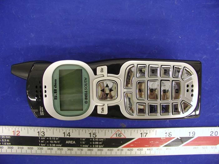
O63GH5850HDLD03
May 23, 2004Digital Cordless Phone � Handset Unit
Equipment Class
DTS - Digital Transmission System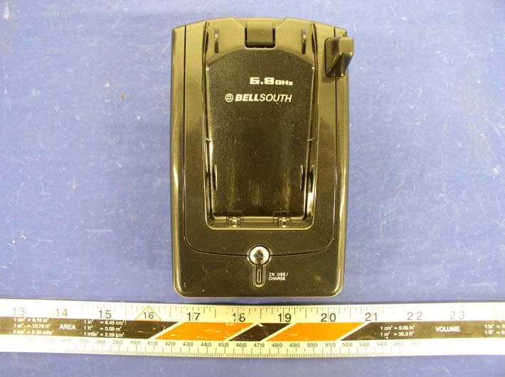
O63GH5815BALD04
Apr 15, 2004Analog Cordless Phone
Equipment Class
DXX - Part 15 Low Power Communication Device Transmitter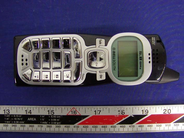
O63GH5815HALD04
Apr 15, 2004Analog Cordless Phone
Equipment Class
DXX - Part 15 Low Power Communication Device Transmitter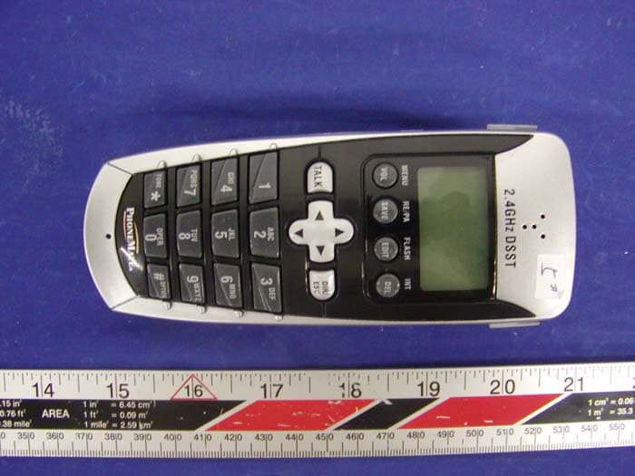
O63PM3320DLD04
Apr 05, 20042.4GHz Digital Spread-Spectrum Cordless Phone
Equipment Class
DTS - Digital Transmission System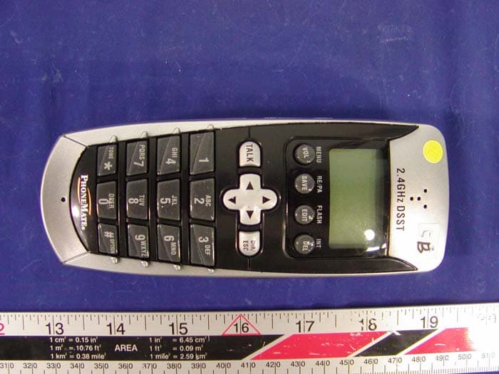
O63PM3375DLD04
Mar 29, 20042.4GHz Digital Spread-Spectrum Cordless Phone
Equipment Class
DTS - Digital Transmission System