O63F29002GMRS Portable Transceiver
Lionda Technology Co Ltd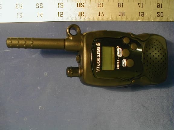
Click to zoom
Application Details
- Equipment Class
- TNF - Licensed Non-Broadcast Transmitter Held to Face
- Date of Grant
- Oct 07, 2001
- Application Purpose
- Original Equipment
- Date of Application
- Oct 07, 2001
- Equipment Note
- GMRS Portable Transceiver
- Frequency Range
- 462.55000000 - 462.72500000
- Company
- Lionda Technology Co Ltd
- Country
- China
Documents & Files
Document Text
Text extracted from the exhibit documents filed with the FCC. Open a document above to read the original.
Users Manual
60mW
Block Diagram
F29002.sch-1 - Thu Aug 23 17:06:06 2001
Cover Letter(s)
September 11, 2001 American TCB: The following information is for our submission on behalf of Lionda Technology Co., Ltd. for its product: FCC ID: O63F29002. Frequency Range (MHz):462.56 – 462.72 Rated RF Output (Watt): 60mW Frequency Tolerance (PPM): 2.3 Emission Designator: 11K0F3E If you have any question, please let me know as soon as possible. Yours truly, John Chan Engi neeri ng Mana ger 230 Commercial St. Ste. Sunnyvale, CA 94085 Tel: (408)732-9162 Fax: (408)732-9164 http://www.baclcorp.com
Cover Letter(s)
American Telecommunications Certification Body Inc. 6731 Whittier Ave, McLean, VA 22101 September 13, 2001 RE: Lionda Technology Co., Ltd. FCC ID: O63F29002 Please review the following comments on this Application. 1.) The test setup for the equipment is in question. This is not a piece of Information Technology equipment; therefore test procedures in ANSI C63.4 are not completely adaptable. For hand held equipment, it is recommended that the equipment be set on the 80 cm table in its vertical position at the table center with microphone cable stretched 1 meter above the tabletop. If this was how it was tested please supply a Test Setup photo. 2.) No RF Exposure information was supplied with this Application. Please submit. 3.) Radiated RF Power Output and Tx Radiated Spurious should exclusively be performed using the substitution method of TIA/EIA 603. 4.) Please provide conducted RF Power Output data in addition to the radiated RF Power Output. This is necessary to assess RF exposure requirements. 5.) Please provide modulated Occupied Bandwidth plots. The graphical presentations shown are without question, not modulated. 6.) Modulation Limiting must be run to at minimum +16dB above reference level used for 1000Hz. 7.) Please provide justification according to Part 2 for your 12K5F3E emission designator. 8.) Please provide signed Form 731. 9.) Form 731 indicates Pout is .057W. Manual supplied indicates two settings: 1.8W high/ .5W low. It is difficult to believe this equipment has a -10dBi negative gain antenna. Please explain. William H. Graff Examining Engineer President and Director of Engineering mailto:[email protected] The items indicated above must be submitted before processing can continue on the above referenced application. Failure to provide the requested information may result in application termination. Correspondence should be considered part of the permanent submission and may be viewed from the Internet after a Grant of Equipment Authorization is issued. Please do not respond to this correspondence using the email reply button. In order for your response to be processed expeditiously, you must submit your documents through the AmericanTCB.com website. Also, please note that partial responses increase processing time and should not be submitted. Any questions about the content of this correspondence should be directed to the sender.
Cover Letter(s)
American Telecommunications Certification Body Inc. 6731 Whittier Ave, McLean, VA 22101 September 24, 2001 RE: Lionda Technology Co., Ltd. FCC ID: O63F29002 There are still a few things missing from this Application. Please address the following deficiencies. 1.) Please provide RF Exposure information. Use Supplement C to OET Bulletin 65 for guidance in evaluating this device for MPE considerations. 2.) Please provide a conducted RF power measurement into a caloric RF power meter or equivalent. This is needed for proper evaluation of RF Exposure report. 3.) Please provide details on antenna type and gain. 4.) Please provide current and voltage measurements through the final amplifier as required under Part 2.1033(c)(8) of the Rules. 5.) Please provide a true updated copy of manual directly from manufacturer. The revised copy sent appears to be cut-and-pasted and is not satisfactory. 6.) The schematic supplied shows this equipment is switchable in power. Further analysis seems to indicate it is very capable of exceeding the requested Pout. Although not required in the documentation list, it would be prudent to submit a copy of the parts list for my evaluation. 7.) Tune up procedure indicates Pout of both 0.5 and 2.0 watts. This is much higher than that requested on Form 731. Please explain. 8.) Modulation limiting plots must show response to excessive audio input on three input frequencies to +20dB above reference obtained at 1000Hz. Please resubmit revised test information. 9.) Test Procedure for ERP in section 4 of report is incorrect. Please review TIA/EIA 603 for proper procedure and review test data. 10.) The Occupied Bandwidth test procedure listed in tour report in Section 6.2 has not been followed. Pleas resubmit Occupied Bandwidth plots. 11.) Please add appropriate masks to all Occupied Bandwidth plots. 12.) The Field Strength of Emissions Section 7 has not been performed in accordance with TIA/EIA 603. Please resubmit. 13.) The Spurious Emission test of Section 8 does not make sense. The references to Intentional and Unintentional Radiators under Part 15 are not appropriate for any Licensed Services. It is unclear what you are trying to demonstrate. William H. Graff Examining Engineer President and Director of Engineering mailto:[email protected] The items indicated above must be submitted before processing can continue on the above referenced application. Failure to provide the requested information may result in application termination. Correspondence should be considered part of the permanent submission and may be viewed from the Internet after a Grant of Equipment Authorization is issued. Please do not respond to this correspondence using the email reply button. In order for your response to be processed expeditiously, you must submit your documents through the AmericanTCB.com website. Also, please note that partial responses increase processing time and should not be submitted. Any questions about the content of this correspondence should be directed to the sender.
External Photos
EUT – Top View EUT – Bottom View
ID Label/Location Info
Proposed FCC ID Labeling Proposed FCC ID Location Back Side of EUT Labeling Requirement Each equipment for which a type acceptance applications is filed on or after May 1, 1981, shall bear an identification plate or label pursuant to §2.295 (Identification of Equipment) and §2.926 (FCC identifier) FCC ID: O63F29002 Proposed FCC ID Location FCC ID: O63F29002
Internal Photos
EUT – Main board Component View EUT – Main Board Solder View
Operational Description
LIONDA TECHNOLOGY COMPANY LIMITED Lionda Research and Development Center F29002 desc Page 1 8/23/01 CIRCUIT DESCRIPTION Model: F29002 a. Receiver Section Radio Frequency signal received by the antenna (ANT1), passing through the Low Pass Filter (L2-L3, C30-C31). The RF signal is then amplified by Low Noise Amplifier Q2 and passes through a Band Pass Filter FL1 (465MHz). The filtered signal within the range of 462 MHz – 467 MHz is then mixed with the first local oscillator signal from the Voltage Controlled Oscillator (VCO) circuit (Q19-Q21, D8, L17) through Q11, a portion of VCO signal is then feedback to the PLL IC (IC5) for phase comparison generating a stable RX Frequency, the output signal is filtered by FL2 (21.7 MHz) which is the first Intermediate Frequency (IF) and is then amplified by Q14. The IF signal is fed to the discriminator IC (IC2) pin 16 which is then mixed with the second local oscillator supplied by crystal X2 (21.25 MHz) to produced and reduced second IF signal. Demodulated signal is recovered through correct adjustment of IF coil (L13) and the internal discriminator circuit of IC2. The recovered Audio signal is outputted at pin 9 of IC2 and then processed through filtering done by U3-D circuit, the fully recovered audio signal is then further amplified by Power Amplifier U3-A. An audible sound is therefore produce by the speaker SPK1, which can be varied from minimum to maximum through the key function (up/down) and process by the CPU IC6. b. Transmitter Section PTT switch when pushed triggers the Transmitter Circuit “ON”, the voice signal generates by the surrounding noise passes through the Microphone MIC1 where mechanical to electrical transformation occurs, the electrical transformed signal is then filtered by a Band Pass Filter U3-A, D, and C. The output signal is Modulated by a modulator circuit with a varactor diode D8 and L17. The external components from Q19-Q21 form a VCO Circuit, which generates the required oscillating frequency for transmission; a portion of this signal is feedback to the PLL IC5 pin 14 for phase comparison in order to produce a stabilized TX frequency. The modulated signal is then amplified by a Cascaded Amplifier Circuit Q17 and Q18 and again amplified by Q24 to produce a sufficient Radio Frequency signal emitted by the Antenna (ANT1). c. Call Transmission By pushing the CALL key, a signal is detected by the CPU (IC6), a CALL data is then produced by the CPU. This data passes through the Band Pass Filter U1-C and modulated by the varactor diode D2 and L8. The signal follows it’s conventional transmission section path through the antenna. d. Continuous Tone Coded Squelch Signal Protocol Once the unit is set to the corresponding Channel and CTCSS code at TX mode a tone is continuously generated from CPU through R96 and R103 and then passes through U1C for filtering and amplification. Then the Coded Tone signal follows its conventional transmission section path. During receiving mode once the Coded Tone signal matched with the set Code the CPU acknowledges and RX mute will disabled and RX will be active LIONDA TECHNOLOGY COMPANY LIMITED Lionda Research and Development Center F29002 desc Page 2 8/23/01 e. Battery Low Detection Battery Low Detection is controlled by the IC6 as detected on the LCD1, however a voltage divider circuit R50 and R51 serve as the stabilize reference voltage for the IC6 to process its detection. f. Squelch Detection Supported by the linear IC circuit (IC2), a variable resistor VR1 sets the level of detection and Diode D11 acts as a comparator circuit interface with the CPU IC6. g. Power Supply Supply voltage of 6 Volts dc is needed to power “ON” the whole circuitry, by four (4) batteries “AAA” size. FREQUENCY CHART CHANNEL NO. FREQUENCY CHANNEL NO. FREQUENCY 1 462.5625 9 462.6250 2 462.5875 10 462.6750 3 462.6125 11 462.5500 4 462.6375 12 462.6000 5 462.6625 13 462.6500 6 462.6875 14 462.7000 7 462.7125 15 462.7250 8 462.5750 CTCSS CODE FREQUENCY CHART CODE FREQUENCY CODE FREQUENCY 1 67.0 20 131.8 2 71.9 21 136.5 3 74.4 22 141.3 4 77.0 23 146.2 5 79.7 24 151.4 6 82.5 25 156.7 7 85.4 26 162.2 8 88.5 27 167.9 9 91.5 28 173.8 10 94.8 29 179.9 11 97.4 30 186.2 12 100.0 31 192.8 13 103.5 32 203.5 14 107.2 33 210.7 15 110.9 34 218.1 16 114.8 35 225.7 17 118.8 36 233.6 18 123.0 37 241.8 19 127.3 38 250.3
Parts List/Tune Up Info
SLC_NPARTGD_NPARTDESCRIPREVQUANTITY 111-1210-016AIC_uP (EMC)78567-LD003H-CIADH DICE FOR FRS1029P01.0000 111-2103-001ASIC-212-0021IC_LI KA3361/MC3361D/SIT336101-S0B0 (SOP)P01.0000 111-2103-005ASIC-212-0067IC_LI KA324/KIA324/LM324(SOP)P03.0000 111-2103-006ASIC-212-0070IC_LI TB31202FN(SOP)P01.0000 111-2103-008ASIC-212-0072IC_LI KA386/LM386(SOP)P01.0000 111-4111-001AIC_MOS VOLTAGE REGULATOR XC62FP4002PR(SOT-89)P01.0000 111-6103-002AIC_MEM 24LC02 (SOIC-8)P01.0000 112-1106-001ASTR-115-0003TR_SS KST2907TF/KTN2907S/AS /MMBT2907LT1(SOT-23)P06.0000 112-1306-001ASTR-125-0008TR_SS KSC1623Y(SOT-23)P06.0000 112-2213-001BTR_RF POWER BFQ540(SOT-89)P01.0000 112-2306-001ASTR-225-0005TR_RF KTC3880Y SOT23P01.0000 112-2306-003BTR_RF 2SC4784 (SOT-23)P05.0000 112-5114-001ATR_MOSFET 2SK3079A (2-5NIA)P01.0000 113-3025-002ASLD-442-H002LED CHIP GREEN ELT-0805GCP01.0000 113-4000-007ALCD XKS2109-TO FOR GMRS F29002P01.0000 114-1109-001ASDD-119-H002DIODE_SW KDS114(URP)P04.0000 114-1207-001ASDD-127-0005DIODE_SW LL4148/MM4148 MELFP04.0000 114-4008-001BSDD-319-H001DIODE_VAR KDV154C(USC)P01.0000 115-0207-8R2ADIODE_ZEN. TZMC8V2 (8.2V/0.5W) MELFP01.0000 122-0224-000AERS-611-0000RES_(0603)-10 0 OHMP08.0000 122-0224-100AERS-611-0100RES_(0603)-10 10 OHMP0###### 122-0224-101AERS-611-0101RES_(0603)-10 100 OHMP03.0000 122-0224-102AERS-611-0102RES_(0603)-10 1 KOHMP0###### 122-0224-103AERS-611-0103RES_(0603)-10 10 KOHMP0###### 122-0224-104AERS-611-0104RES_(0603)-10 100 KOHMP01.0000 122-0224-104AERS-611-0104RES_(0603)-10 100 KOHMP06.0000 122-0224-105AERS-611-0105RES_(0603)-10 1 MOHMP02.0000 122-0224-122AERS-611-0122RES_(0603)-10 1.2 KOHMP02.0000 122-0224-123AERS-611-0123RES_(0603)-10 12 KOHMP02.0000 122-0224-124AERS-611-0124RES_(0603)-10 120 KOHMP02.0000 122-0224-152AERS-611-0152RES_(0603)-10 1.5 KOHMP01.0000 122-0224-153AERS-611-0153RES_(0603)-10 15 KOHMP03.0000 122-0224-182AERS-611-0182RES_(0603)-10 1.8 KOHMP01.0000 122-0224-183AERS-611-0183RES_(0603)-10 18 KOHMP02.0000 122-0224-184AERS-611-0184RES_(0603)-10 180 KOHMP01.0000 122-0224-202ARES_(0603)-10 2 KOHMP01.0000 122-0224-222AERS-611-0222RES_(0603)-10 2.2 KOHMP08.0000 122-0224-223AERS-611-0223RES_(0603)-10 22 KOHMP0###### 122-0224-223AERS-611-0223RES_(0603)-10 22 KOHMP00.0000 122-0224-224AERS-611-0224RES_(0603)-10 220 KOHMP0###### 122-0224-224AERS-611-0224RES_(0603)-10 220 KOHMP00.0000 122-0224-273AERS-611-0273RES_(0603)-10 27 KOHMP05.0000 122-0224-330AERS-611-0330RES_(0603)-10 33 OHMP06.0000 122-0224-331AERS-611-0331RES_(0603)-10 330 OHMP02.0000 122-0224-332AERS-611-0332RES_(0603)-10 3.3 KOHMP01.0000 122-0224-333AERS-611-0333RES_(0603)-10 33 KOHMP05.0000 122-0224-334AERS-611-0334RES_(0603)-10 330 KOHMP05.0000 122-0224-393AERS-611-0393RES_(0603)-10 39 KOHMP02.0000 122-0224-471AERS-611-0471RES_(0603)-10 470 OHMP01.0000 122-0224-472AERS-611-0472RES_(0603)-10 4.7 KOHMP0###### 122-0224-473AERS-611-0473RES_(0603)-10 47 KOHMP08.0000 122-0224-474AERS-611-0474RES_(0603)-10 470 KOHMP04.0000 122-0224-513AERS-611-0513RES_(0603)-10 51 KOHMP01.0000 122-0224-560AERS-611-0560RES_(0603)-10 56 OHMP02.0000 122-0224-561AERS-611-0561RES_(0603)-10 560 OHMP01.0000 122-0224-562AERS-611-0562RES_(0603)-10 5.6 KOHMP04.0000 122-0224-563AERS-611-0563RES_(0603)-10 56 KOHMP01.0000 122-0224-564AERS-611-0564RES_(0603)-10 560 KOHMP01.0000 122-0224-682AERS-611-0682RES_(0603)-10 6.8 KOHMP06.0000 122-0224-683AERS-611-0683RES_(0603)-10 68 KOHMP03.0000 122-0224-684AERS-611-0684RES_(0603)-10 680 KOHMP01.0000 122-0224-820AERS-611-0820RES_(0603)-10 82 OHMP01.0000 122-0224-822AERS-611-0822RES_(0603)-10 8.2 KOHMP02.0000 122-0224-823AERS-611-0823RES_(0603)-10 82 KOHMP03.0000 123-3224-503AERV-263-0503CHIP SVR 50 KOHMP02.0000 123-4713-103AROTARY SVR. 15KC-B 10 KOHMP01.0000 124-3140-003AEHS-300-H001CHIP SPRING COIL D1.2X0.32X3TP05.0000 124-3140-004AEHS-300-H002CHIP SPRING COIL D1.2X0.32X4TP05.0000 124-3140-005AEHS-300-H003CHIP SPRING COIL D1.2X0.32X5TP03.0000 124-3352-S22AEHS-123-0220CHIP COIL SQUARE 22nH/K(0603)P02.0000 124-3362-2R2AEHS-134-0222CHIP COIL SQUARE 2.2uH/K(0805)P01.0000 126-0102-001AIFT COIL 224-005SP01.0000 127-6300-070ACAP_C_TRIMMER 7PF JTC06A07P01.0000 128-1211-010AECS-310-0010CAP_C CHIP 1PF/B/(CH)/(0603) A:COG150LP01.0000 128-1212-020AECS-311-0020CAP_C CHIP 2PF/C/(CH)/(0603) A:COG150LP02.0000 128-1213-040AECS-312-0040CAP_C_CHIP 4PF/D(CH)(0603) A:COG150LP01.0000 128-1213-050AECS-312-0050CAP_C_CHIP 5PF/D(CH)(0603) A:COG150LP03.0000 128-1213-070AECS-312-0070CAP_C_CHIP 7PF/D(CH)(0603) A:COG150LP03.0000 128-1213-080AECS-312-0080CAP_C_CHIP 8PF/D(CH)(0603) A:COG150LP02.0000 128-1213-100AECS-312-0100CAP_C CHIP 10PF/D/(CH)/(0603) A:COG150LP05.0000 128-1213-2R5ACAP_C_CHIP 2.5PF/D(CH)(0603) A:COG150LP01.0000 128-1213-3R3ACAP_C_CHIP 3.3PF/D(CH)(0603) A:COG150LP03.0000 128-1216-101AECS-314-0101CAP_C_CHIP 100PF/J(CH)(0603) A:COG150LP0###### 128-1216-120AECS-314-0120CAP_C_CHIP 12PF/J(CH)(0603) A:COG150LP01.0000 128-1216-150AECS-314-0150CAP_C_CHIP 15PF/J(CH)(0603) A:COG150LP02.0000 128-1216-200AECS-314-0200CAP_C_CHIP 20PF/J(CH)(0603) A:COG150LP03.0000 128-1216-220AECS-314-0220CAP_C_CHIP 22PF/J(CH)(0603) A:COG150LP01.0000 128-1216-221AECS-314-0221CAP_C_CHIP 220PF/J(CH)(0603) A:COG150LP09.0000 128-1216-300AECS-314-0300CAP_C_CHIP 30PF/J(CH)(0603) A:COG150LP02.0000 128-1216-471AECS-314-0471CAP_C_CHIP 470PF/J(CH)(0603) A:COG150LP02.0000 128-1216-561AECS-314-0561CAP_C_CHIP 560PF/J(CH)(0603) A:COG150LP03.0000 128-1216-681ACAP_C_CHIP 680PF/J(CH)(0603) A:COG150LP01.0000 128-1216-820AECS-314-0820CAP_C_CHIP 82PF/J(CH)(0603) A:COG150LP01.0000 128-2297-102AECS-555-0102CAP_C_C.H.D. B0.001uF/K(0603) X:X7R282LP08.0000 128-2297-103AECS-555-0103CAP_C_C.H.D. B0.01uF/K(0603) X:X7R282LP0###### 128-2297-153AECS-555-0153CAP_C_C.H.D. B0.015uF/K(0603) X:X7R282LP01.0000 128-2297-222AECS-555-0222CAP_C_C.H.D. B0.0022uF/K(0603) X:X7R282LP01.0000 128-2297-223AECS-555-0223CAP_C_C.H.D. B0.022uF/K(0603) X:X7R282LP04.0000 128-2297-332AECS-555-0332CAP_C_C.H.D. B0.0033uF/K(0603) X:X7R282LP01.0000 128-2297-472AECS-555-0472CAP_C_C.H.D. B0.0047uF/K(0603) X:X7R…
Text truncated - open the document above for the full version.
RF Exposure Info
1. antenna type and gain ELECTRICAL CHARACTERISTICS - resonate frequency : 462 MHz +/-10MHz - impedance : 50 ohms nominal - radiation pattern : omni directional - polariztion : Vertical - s. w. r. : 2.0 or less - gain : 1.64 - storage temp. : -30°C to 70°C - operating temp. : -20°C to 60° - dielectric strength : AC 1500V for one minute - Insulation resistance : 100Mohms at DC 500V - humidity resistance : satisfy the electrical and mechanical characteristics after 6 hours in 95% RH at 40°C and one hour dying. - vibration resistance : satisfy the electrical and mechanical characteristics after two hours in each 3 dimension with 10-55 hz amplitude 105mm and interval one minute. - shock resistance : satisfy the electrical and mechanical characteristics after drop down with 100g upon rubber block.
Schematics
F2009.SCH-2 - Thu Aug 23 18:04:06 2001 F29002SCH.sch-1 - Thu Aug 23 11:18:49 2001
Schematics
F2009.SCH-2 - Thu Aug 23 18:04:06 2001 F29002SCH.sch-1 - Thu Aug 23 11:18:49 2001
Test Report
2. reading for rf final amplifier. - DC voltage : 6V - DC current : 800mA
Test Report
Note: This report may not be duplicated without prior written consent of Bay Area Compliance Laboratory Corporation. This report must not be used by the client to claim product endorsement by NVLAP or any agency of the U.S. Government. FCC PART 95 EMI MEASUREMENT AND TEST REPORT For Lionda Technology Co., Ltd. Block 2 Laodong 2 nd Industrial Area, Xixiang, Baoan, Shenzhen, Guangdong, P.R.China FCC ID: O63F29002 September 6, 2001 This Report Concerns: Original Report Equipment Type: Family Radio Transmitter, Personal Radio Service Test Engineer: Jeff Lee Test Date: August 21, 2001 Reviewed By: John Y. Chan – Engineering Manager Prepared By: Bay Area Compliance Laboratory Corporation 230 Commercial Street, Suite 2 Sunnyvale, CA 94085 Tel: (408) 732-9162 Fax: (408) 732 9164 Lionda Technology Co., Ltd. FCC ID: O63F29002 Report # R0108215 FCC Part 95 Test Report Page 2 of 33 TABLE OF CONTENTS 1 - GENERAL INFORMATION.................................................................................................................................................4 1.1 PRODUCT DESCRIPTION FOR EQUIPMENT UNDER TEST (EUT)........................................................................................4 1.2 OBJECTIVE................................................................................................................................................................................4 1.3 TEST METHODOLOGY..............................................................................................................................................................4 1.4 TEST FACILITY.........................................................................................................................................................................4 1.5 TEST EQUIPMENT LIST............................................................................................................................................................5 1.6 EQUIPMENT UNDER TEST (EUT)...........................................................................................................................................5 1.7 LOCAL SUPPORT EQUIPMENT LIST AND DETAILS...............................................................................................................5 1.8 EXTERNAL I/O CABLES LIST AND DETAILS.........................................................................................................................5 2 - SYSTEM TEST CONFIGURATION..................................................................................................................................6 2.1 JUSTIFICATION..........................................................................................................................................................................6 2.2 EUT EXERCISE SOFTWARE....................................................................................................................................................6 2.3 SPECIAL ACCESSORIES............................................................................................................................................................6 2.4 SCHEMATICS / BLOCK DIAGRAM...........................................................................................................................................6 2.5 EQUIPMENT MODIFICATIONS.................................................................................................................................................6 2.6 CONFIGURATION OF TEST SYSTEM.......................................................................................................................................7 2.7 TEST SETUP BLOCK DIAGRAM...............................................................................................................................................7 3 – REQUIREMENTS OF PROVISIONS...............................................................................................................................8 3.1 DEFINITION...............................................................................................................................................................................8 3.2 REQUIREMENTS AND TEST SUMMARY..................................................................................................................................8 3.3 LABELING REQUIREMENT.......................................................................................................................................................8 4 – EFFECTIVE RADIATED POWER....................................................................................................................................9 4.1 PROVISION APPLICABLE.........................................................................................................................................................9 4.2 TEST PROCEDURE....................................................................................................................................................................9 4.3 TEST EQUIPMENT......................................................................................................................................................................9 4.4 TEST RESULTS..........................................................................................................................................................................9 5 - MODULATION CHARACTERISTICS...........................................................................................................................13 5.1 PROVISION APPLICABLE.......................................................................................................................................................13 5.2 TEST PROCEDURE..................................................................................................................................................................13 5.3 TEST EQUIPMENT...................................…
Text truncated - open the document above for the full version.
Test Setup Photos
Radiated Emission Setup - Front View Radiated Emission Setup - Rear View
Contact Information
Applicant
Dan Coronia(Senior Engineer)
Technical Contact
Bay Area Compliance LaboratoryJohn Chan
[email protected]408 732 9162
230 Commercial St. Ste. 2 · Sunnyvale, California · United States
Non-Technical Contact
Bay Area Compliance LaboratoryRita Cai
[email protected]408 732 9162
Test Firm
Bay Area Compliance LaboratoryJohn Chan
Technical Specifications
| # | Rule Parts | Frequency Range | Power Output | Emission | Tolerance |
|---|---|---|---|---|---|
| 1 | 95A | 462.55 MHz - 462.725 MHz | 60.00 mW | 11K0F3E | 2.3000000000 ppm |
Other Applications from Lionda Technology Co Ltd
O63GH5850HDLD03
May 23, 2004Digital Cordless Phone � Handset Unit
Equipment Class
DTS - Digital Transmission System
O63GH5815BALD04
Apr 15, 2004Analog Cordless Phone
Equipment Class
DXX - Part 15 Low Power Communication Device Transmitter
O63GH5815HALD04
Apr 15, 2004Analog Cordless Phone
Equipment Class
DXX - Part 15 Low Power Communication Device Transmitter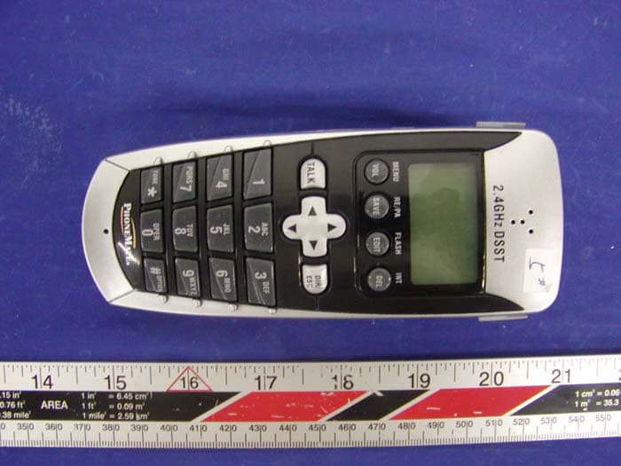
O63PM3320DLD04
Apr 05, 20042.4GHz Digital Spread-Spectrum Cordless Phone
Equipment Class
DTS - Digital Transmission System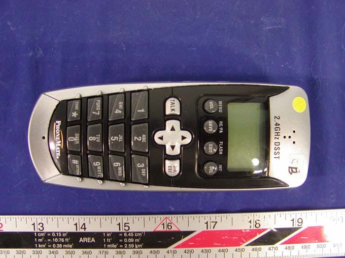
O63PM3375DLD04
Mar 29, 20042.4GHz Digital Spread-Spectrum Cordless Phone
Equipment Class
DTS - Digital Transmission System