O78SC280AVHF PORTABLE RADIO
Smart Communications Ltd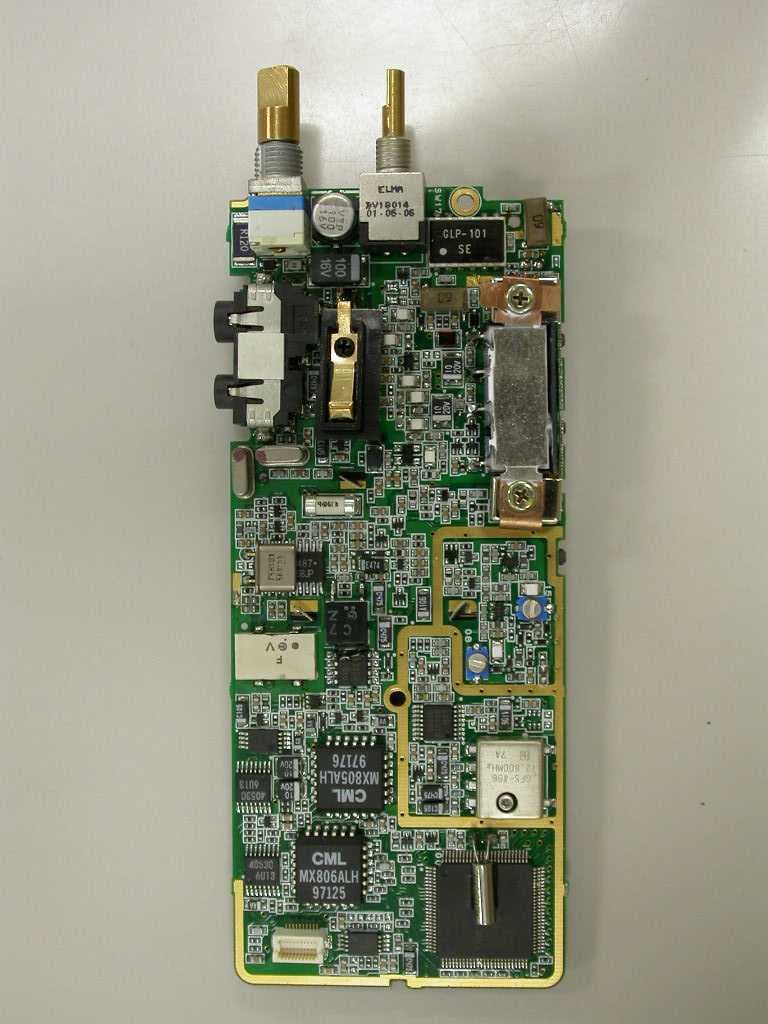
Click to zoom
Application Details
- Equipment Class
- TNF - Licensed Non-Broadcast Transmitter Held to Face
- Date of Grant
- Dec 27, 2007
- Application Purpose
- Original Equipment
- Date of Application
- Dec 23, 2007
- Equipment Note
- VHF PORTABLE RADIO
- Frequency Range
- 136.00000000 - 174.00000000
- Company
- Smart Communications Ltd
- Country
- Hong Kong
Documents & Files
Document Text
Text extracted from the exhibit documents filed with the FCC. Open a document above to read the original.
Users Manual
Page 1/11 INSTRUCTION MANUAL SC- 580, SC- 581 series UHF TRUNKING / CONVENTIONAL TRANSCEIVER SC- 280, SC- 281 series VHF TRUNKING / CONVENTIONAL TRANSCEIVER Page 2/11 - FCC NOTICE - SAFETY INFORMATION This radio is restricted to occupational use, work related operations only where the radio operator must have the knowledge to control its RF exposure conditions. When the Push-to-Talk (PTT) button is pushed, the transceiver sends out radio frequency (RF) signals. In August 1996, the Federal Communications Commission adopted RF exposure guidelines with safety levels for hand-held wireless devices. The device is authorized to operate at a duty factor not to exceed 50%. WARNING To maintain compliance with the FCC’s RF exposure guidelines, this transmitter and its Antenna must maintain a separation distance of at least 1 inch (2.5 centimeters) from your face and body.. Speak in a normal voice, with the antenna pointed up and away from the face at the required separation distance. NOTICE This equipment has been tested and found to comply with the limits for a Class B digital device, pursuant to Part 15 of the FCC Rules. These limits are designed to provide reasonable protection against harmful interference in a reasonable installation. This equipment generates, uses and can radiate radio frequency energy and, if not installed and used in accordance with the instructions, may cause harmful interference to radio communications. However, there is no guarantee that interference will not occur in a particular installation. If this equipment does cause harmful interference to radio or television reception, which can be determined by turning the equipment off and on, the user is encouraged to try to correct the interference by one or more of the following measures: - Increase the separation between the equipment and receiver. - Connect the equipment into an outlet on a circuit different from that to which the receiver is connected. - Consult the dealer or an experienced electronics technician for help. Page 3/11 CONTENTS GENERAL INFORMATION................................................................................4 SUPPLIED ACCESSORIES................................................................................................4 ACCESSORY ATTACHMENTS.........................................................................4 INSTALLING THE ANTENNA.........................................................................................4 INSTALLING / REMOVING THE BATTERY PACK........................................................5 INSTALLING THE BELT CLIP........................................................................................5 INSTALLING THE JACK COVER...................................................................................5 BATTERY SAFETY............................................................................................5 USING THE BATTERY PACK.............................................................................................6 INSTALLING / REMOVING THE BATTERY PACK............................................................6 BATTERY LIFE INDICATOR...............................................................................................6 CONTROL AND CONNECTIONS......................................................................7 POWER SWITCH / VOLUME CONTROL...........................................................................7 SYSTEM/GROUP CONTROL.............................................................................................7 TX/BUSY LED INDICATOR................................................................................................7 LCD (Liquid Crystal Display)............................................................................................7 H (HOME) KEY....................................................................................................................8 S (SCAN) KEY.....................................................................................................................8 F1 KEY.................................................................................................................................8 F2 KEY.................................................................................................................................8 10 KEY (SC- 580, SC-280 full key model only)................................................................8 PTT SWITCH.......................................................................................................................8 SHIFT (shift/key lock) KEY................................................................................................8 PROGRAMMABLE KEY FUNCTIONS...............................................................................9 ACCESSORY JACK............................................................................................................9 BATTERY PACK..................................................................................................................9 BATTERY LOCK.................................................................................................................9 ADJUST THE LCD CONTRAST.........................................................................................9 BASIC OPERATION........................................................................................10 LTR OPERATION..............................................................................................................10 CONVENTIONAL OPERATION........................................................................................10 EMERGENCY....................................................................................................................11 OPTION.............................................................................................................................11 Page 4/11 GENERAL INFORMATION The SC-580 series and SC-280 series transceiver is a combination conven…
Text truncated - open the document above for the full version.
Attestation Statements
December 21, 2007 Federal Communications Commission Re: FCC ID O78SC280A Applicant: Smart Communications LTD Subject: justification letter for expanded frequency range 136 - 174 MHz To Whom It May Concern: You have asked Smart Communications for justification to have the 136-174 MHz freq range appear on he face of the FCC Grant of Certification for a Part 90 Certification. This frequency range is regarded as usual & customary by United States Federal Government and its various departments, user organizations and the military to appear on the face of the equipment Grant of Certification. (1) Smart Communications Marketing Department plans to ensure that USA users, other than those specifically identified in this letter, not operate within bands 136-150 MHz, as controlled by the users’ FCC station license. (2) This device will not be marketed to USA users, other than those identified in the letter, namely the US Government and its various departments & military, for operation in 136-150 MHz frequency range. Sincerely, Sincerely, Walter “Bud” Simciak Chief Engineer, ADRad Communications, Inc. 5481 SAND LAKE DRIVE, MELBOURNE,FLORIDA • 32934 PHONE/FAX: 321-255-0329
Block Diagram
I. MICROPHONE MATCHING NETWORK Figure 1 MICROPHONE MATCHING NETWORK MIC INPUT GND PTT EXT PTT SWITCH 100uF/16V GND PTT MIC INPUT AUDIO GENERATOR
Cover Letter(s)
5481 SAND LAKE DRIVE, MELBOURNE,FLORIDA • 32934 PHONE/FAX: 321-255-0329 December 28, 2007 Federal Communications Commission Re: FCC ID O78SC280A Applicant: Smart Communications LTD To Whom It May Concern: Our client, Smart Communications LTD has requested that the following information is to be held confidential and on their behalf: Block Diagram Schematic Diagram Operational Description Parts List Tune Up Procedures . These exhibits were marked confidential at time of upload. Smart Communications deems this information to be a trade secret and proprietary. If made public, this information would damage their position in the market place. Sincerely, Walter “Bud” Simciak Chief Engineer, ADRad Communications, Inc.
External Photos
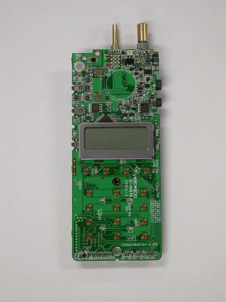
E. PHOTOGRAPHS-SC-280 A With Battery (SCB-2200) 1) Model view of SC-280 A – Front Three- Quarter View 1 2) Model view of SC-280 A – Front Three- Quarter View 2 3) Model view of SC-280 A – Back view 4) Model view of SC-280 A – Back view (Label Position) 5) Model view of SC-280 A – Top view 6) Model view of SC-280 A – Bottom view 7) Model view of SC-280 A – Belt clip 1 8) Model view of SC-280 A – Belt clip 2 9) MAIN PCB of SC-280 A (Component Side View) 10) MAIN PCB of SC-280 A (Solder Side View) 1) Model view of SC-280 A – Front Three- Quarter View 1 2) Model view of SC-280 A – Front Three- Quarter View 2 3) Model view of SC-280 A – Back view 4) Model view of SC-280 A – Back view (Label Position) 5) Model view of SC-280 A – Top view 6) Model view of SC-280 A – Bottom view 7) Model view of SC-280 A – Belt clip 1 8) Model view of SC-280 A – Belt clip 2 9) MAIN PCB of SC-280 A (Component Side View) 10) MAIN PCB of SC-280 A (Solder Side View) E. PHOTOGRAPHS-SC-280 A With Battery (SCB-4000) 1) Model view of SC-280 A – Front Three- Quarter View 1 2) Model view of SC-280 A – Front Three- Quarter View 2 3) Model view of SC-280 A – Back view 4) Model view of SC-280 A – Top view 5) Model view of SC-280 A – Bottom view 6) Model view of SC-280 A – Belt clip 1 7) Model view of SC-280 A – Belt clip 2 1) Model view of SC-280 A – Front Three- Quarter View 1 2) Model view of SC-280 A – Front Three- Quarter View 2 3) Model view of SC-280 A – Back view 4) Model view of SC-280 A – Top view 5) Model view of SC-280 A – Bottom view 6) Model view of SC-280 A – Belt clip 1 7) Model view of SC-280 A – Belt clip 2
External Photos
E. PHOTOGRAPHS-SC-281 A With Battery (SCB-2200) 1) Model view of SC-281 A – Front Three- Quarter View 1 2) Model view of SC-281 A – Front Three- Quarter View 2 3) Model view of SC-281 A – Back view 4) Model view of SC-281 A – Back view (Label Position) 5) Model view of SC-281 A – Top view 6) Model view of SC-281 A – Bottom view 7) Model view of SC-281 A – Belt clip 1 8) Model view of SC-281 A – Belt clip 2 9) MAIN PCB of SC-281 A (Component Side View) 10) MAIN PCB of SC-281 A (Solder Side View) 1) Model view of SC-281 A – Front Three- Quarter View 1 2) Model view of SC-281 A – Front Three- Quarter View 2 3) Model view of SC-281 A – Back view 4) Model view of SC-281 A – Back view (Label Position) 5) Model view of SC-281 A – Top view 6) Model view of SC-281 A – Bottom view 7) Model view of SC-281 A – Belt clip 8) Model view of SC-281 A – Belt clip 2 9) MAIN PCB of SC-281 A (Component Side View) 10) MAIN PCB of SC-281 A (Solder Side View) E. PHOTOGRAPHS-SC-281 A With Battery (SCB-4000) 1) Model view of SC-281 A – Front Three- Quarter View 1 2) Model view of SC-281 A – Front Three- Quarter View 2 3) Model view of SC-281 A – Back view 4) Model view of SC-281 A – Top view 5) Model view of SC-281 A – Bottom view 6) Model view of SC-281 A – Belt clip 1 7) Model view of SC-281 A – Belt clip 2 1) Model view of SC-281A – Front Three- Quarter View 1 2) Model view of SC-281 A – Front Three- Quarter View 2 3) Model view of SC-281 A – Back view 4) Model view of SC-281 A – Top view 5) Model view of SC-281 A – Bottom view 6) Model view of SC-281 A – Belt clip 1 7) Model view of SC-281 A – Belt clip 2
ID Label/Location Info
MODEL LABEL DETAIL FCC Operational Requirement Radio intended for occupational Push to Talk service only. Required training is in the instruction manual which must be reviewed prior to operation. THIS DEVICE COMPLIES WITH PART 15 OF THE FCC RULES. OPERATION IS SUBJECT TO THE CONDITION THAT THIS DEVICE DOES NOT CAUSE HARMFUL INTERFERENCE. SC - 280A / SC - 281A MODEL LABEL POSITION Rear side panel Label
Internal Photos
E. PHOTOGRAPHS-SC-280 A With Battery (SCB-2200) 1) Model view of SC-280 A – Front Three- Quarter View 1 2) Model view of SC-280 A – Front Three- Quarter View 2 3) Model view of SC-280 A – Back view 4) Model view of SC-280 A – Back view (Label Position) 5) Model view of SC-280 A – Top view 6) Model view of SC-280 A – Bottom view 7) Model view of SC-280 A – Belt clip 1 8) Model view of SC-280 A – Belt clip 2 9) MAIN PCB of SC-280 A (Component Side View) 10) MAIN PCB of SC-280 A (Solder Side View) 1) Model view of SC-280 A – Front Three- Quarter View 1 2) Model view of SC-280 A – Front Three- Quarter View 2 3) Model view of SC-280 A – Back view 4) Model view of SC-280 A – Back view (Label Position) 5) Model view of SC-280 A – Top view 6) Model view of SC-280 A – Bottom view 7) Model view of SC-280 A – Belt clip 1 8) Model view of SC-280 A – Belt clip 2 9) MAIN PCB of SC-280 A (Component Side View) 10) MAIN PCB of SC-280 A (Solder Side View) E. PHOTOGRAPHS-SC-280 A With Battery (SCB-4000) 1) Model view of SC-280 A – Front Three- Quarter View 1 2) Model view of SC-280 A – Front Three- Quarter View 2 3) Model view of SC-280 A – Back view 4) Model view of SC-280 A – Top view 5) Model view of SC-280 A – Bottom view 6) Model view of SC-280 A – Belt clip 1 7) Model view of SC-280 A – Belt clip 2 1) Model view of SC-280 A – Front Three- Quarter View 1 2) Model view of SC-280 A – Front Three- Quarter View 2 3) Model view of SC-280 A – Back view 4) Model view of SC-280 A – Top view 5) Model view of SC-280 A – Bottom view 6) Model view of SC-280 A – Belt clip 1 7) Model view of SC-280 A – Belt clip 2
Internal Photos
E. PHOTOGRAPHS-SC-281 A With Battery (SCB-2200) 1) Model view of SC-281 A – Front Three- Quarter View 1 2) Model view of SC-281 A – Front Three- Quarter View 2 3) Model view of SC-281 A – Back view 4) Model view of SC-281 A – Back view (Label Position) 5) Model view of SC-281 A – Top view 6) Model view of SC-281 A – Bottom view 7) Model view of SC-281 A – Belt clip 1 8) Model view of SC-281 A – Belt clip 2 9) MAIN PCB of SC-281 A (Component Side View) 10) MAIN PCB of SC-281 A (Solder Side View) 1) Model view of SC-281 A – Front Three- Quarter View 1 2) Model view of SC-281 A – Front Three- Quarter View 2 3) Model view of SC-281 A – Back view 4) Model view of SC-281 A – Back view (Label Position) 5) Model view of SC-281 A – Top view 6) Model view of SC-281 A – Bottom view 7) Model view of SC-281 A – Belt clip 8) Model view of SC-281 A – Belt clip 2 9) MAIN PCB of SC-281 A (Component Side View) 10) MAIN PCB of SC-281 A (Solder Side View) E. PHOTOGRAPHS-SC-281 A With Battery (SCB-4000) 1) Model view of SC-281 A – Front Three- Quarter View 1 2) Model view of SC-281 A – Front Three- Quarter View 2 3) Model view of SC-281 A – Back view 4) Model view of SC-281 A – Top view 5) Model view of SC-281 A – Bottom view 6) Model view of SC-281 A – Belt clip 1 7) Model view of SC-281 A – Belt clip 2 1) Model view of SC-281A – Front Three- Quarter View 1 2) Model view of SC-281 A – Front Three- Quarter View 2 3) Model view of SC-281 A – Back view 4) Model view of SC-281 A – Top view 5) Model view of SC-281 A – Bottom view 6) Model view of SC-281 A – Belt clip 1 7) Model view of SC-281 A – Belt clip 2
Operational Description
Page 1/1 SPECIFICATIONS – SC- 280A, SC- 281 A Parameter Specification General Emission Designator : 11K0F3E / 16K0F3E Channel spacing : 12.5 kHz/ 25 kHz Power supply voltage : 7.2V +/-15% Current consumption (Standby) : 70mA (RX) : 300mA (at Maximum Audio output) (TX) : 1.9A (at High Power); 1.2A (at Low Power) Dimensions (inches) : 5.11”H x 2.41”W x 1.42”D Projectionnotincluded (130H x 61.25W x 36D mm) Weightw/oBattery : 0.44lb (200g) Operating Temperature :-30 to +60 degrees Celsius Transmitter Frequency range : 136.000 to 156.000MHz RF power output ([email protected]) : 5W ([email protected]) : 1W Conducted spurious emissions : >60dB AF distortion (@1kHz) : <5% Maximum deviation : +/-2.5 kHz / +/-5kHz Frequency stability : +/-2.5ppm FM noise : >40dB Microphone type : Condenser Microphone impedance : 2000 ohms Receiver Frequency range : 136.000 to 156.000MHz Circuit type : Double-conversion super heterodyne Intermediate Frequency (1st) : 44.95MHz (Upper) (2nd) : 455kHz (Lower) Reference sensitivity (12dB SINAD) : 0.28uV Adjacent channel selectivity : >60dB Inter modulation response : >60dB Spurious response rejection : >65dB Speaker Impedance (Rated) : 8 ohms Maximum AF output (@ 8ohm, 7.2V) : >500mW
Test Report
TECHNICAL REPORT FOR TYPE ACCEPTANCE OF SMART COMMUNICATIONS, LTD. MODEL : SC-280A, SC-281A FCC ID : O78SC280A EMI TEST REPORT Date of test : May 11, 2007 UL Japan, Inc. YAMAKITA EMC LAB. 907 Kawanishi, Yamakita-machi, Ashigarakami-gum, Kanagawa-ken, 258-0124 JAPAN TECHNICAL DATA – SC- 280 A, SC- 281 A Narrow band A. RF POWER OUTPUT 1. Power measured using test set-up Figure 1. Primary power 7.2 VDC at battery input connector. 2. Power Data for 136.0125MHz to 155.9875MHz @ 5W is presented in Paragraph 1. 3. Power Data for 136.0125MHz to 155.9875MHz @ 1W is presented in Paragraph 2. B. FREQUENCY STABILITY 1. a. Frequency stability with varying temperature. See Figure 1 for test set-up. b. Data is presented on Paragraph 3 for Standard Primary Input Voltage of 7.2 VDC maintained throughout entire test. 2. a. Frequency stability with Primary Input Voltage. See Figure 1 for test set-up. b. Data is presented on Paragraph 4 for Standard Temperature of 25 degrees Celsius maintained throughout entire test. C. OCCUPIED BANDWIDTH 1. a. A spectrum analyzer was used to determine the occupied bandwidth. See Figure 1 for test set-up. b. Data is presented on Paragraph 5 to Paragraph 8 for Standard primary Input Voltage of 7.2 VDC maintained throughout entire test. The carrier and all detectable sidebands were displayed on the spectrum analyzer and pertinent data concerning amplitude and frequency were read from the screen. c. un modulated : Data measured at 146.0125MHz. (see Paragraph 5) d. Input to transmitter audio circuits: 2500Hz sine wave at a level 16dB greater than that necessary to produce 50% modulation. Data measured at 146.0125MHz and is typical of all frequencies. (see Paragraph 6) e. Input to transmitter audio circuits: 2500Hz sine wave at a level 16dB greater than that necessary to produce 50% modulation with CTCSS(250.3Hz). Data measured at 146.0125MHz and is typical of all frequencies. (see Paragraph 7) f. Input to transmitter audio circuits: 2500Hz sine wave at a level 16dB greater than that necessary to produce 50% modulation with DCS(023). Data measured at 146.0125MHz and is typical of all frequencies. (see Paragraph 8) D. MODULATION CHARACTERISTICS 1. Modulation Deviation a. Measured using test set-up, see Figure 1. b. Primary Input Voltage of 7.2 VDC at battery input connector. c. Data (Positive peak) is presented in Paragraph 9 d. Data (Negative peak) is presented in Paragraph 10. e. Data (Positive peak) with CTCSS (250.3Hz) is presented in Paragraph 11. f. Data (Negative peak) with CTCSS (250.3Hz) is presented in Paragraph 12. g. Data (Positive peak) with DCS (023) is presented in Paragraph 13. h. Data (Negative peak) with DCS (023) is presented in Paragraph 14. 2. Transmitter Audio Frequency Response a. Measured using test set-up, see Figure 1. b. Primary Input Voltage of 7.2 VDC at battery input connector. Ref = 1 kHz tone response at +-1.5 kHz deviation. Curve was taken maintaining constant +- 1.5 kHz deviation. c. Data is presented in Paragraph 15. 3. Low-Pass Filter Response a. Measured using test set-up, see Figure 1. b. Primary Input Voltage of 7.2 VDC at battery input connector. Input 1 kHz tone at a level 20dB greater than that required for 3 kHz deviation The response at 1 kHz tone = 0dB. Curve was taken maintaining constant input at modulation sensitivity. Output of low-pass filter was monitored using Audio Analyzer c. Data is presented in Paragraph 16. E. CONDUCTED SPURIOUS EMISSION 1. Conducted spurious data was measured at 25 degrees Celsius, 7.2 VDC applied at battery input connector external power input and using external antenna jack. See Figure 1 for test set-up. 2. Data for 136.0125MHz @ 5W is presented in Paragraph 17. 3. Data for 146.0125MHz @ 5W is presented in Paragraph 18. 4. Data for 155.9875MHz @ 5W is presented in Paragraph 19. 5. Data for 136.0125MHz @ 1W is presented in Paragraph 20. 6. Data for 146.0125MHz @ 1W is presented in Paragraph 21. 7. Data for 155.9875MHz @ 1W is presented in Paragraph 22. 8. Data for 146.0125MHz @ Receiver is presented in Paragraph 23. F. TRANSIENT BEHAVIOR a. Measured using test set-up, see Figure 1. b. Primary Input Voltage of 7.2 VDC at battery input connector. c. Data is presented in Paragraph 24. G. RADIATED SPURIOUS EMISSION 1. Radiated spurious data was measured at 20degrees Celsius, 7.2 VDC applied at battery input and using external antenna jack into a 50 ohm non-radiating load. The substitution method found in TIA/EIA 603 procedure. 2. Data for 136.0125MHz @ 5W is presented in Paragraph 25. 3. Data for 146.0125MHz @ 5W is presented in Paragraph 26. 4. Data for 155.9875MHz @ 5W is presented in Paragraph 27. H. RADIATED SPURIOUS EMISSION (Receive) 1. Data for 136.0125MHz to 155.9875MHz @ Receiver is presented in Sheet 1. EMI TEST REPORT I. PARAGRAPHS 1. RF Power Output, 5W 2. RF Power Output, 1W 3. Frequency Stability vs. Temperature 4. Frequency Stability vs. Voltage 5. Occupied Bandwidth, un modulated 6. Occupied Bandwidth, 2500Hz Sine Wave 7. Occupied Bandwidth, 2500Hz Sine Wave with CTCSS (250.3Hz) 8. Occupied Bandwidth, 2500Hz Sine Wave with DCS (023) 9. Deviation vs. Audio input Level - Positive peak 10. Deviation vs. Audio input Level - Negative peak 11. Deviation vs. Audio input Level with CTCSS (250.3Hz) - Positive peak 12. Deviation vs. Audio input Level with CTCSS (250.3Hz) - Negative peak 13. Deviation vs. Audio input Level with DCS (023) - Positive peak 14. Deviation vs. Audio input Level with DCS (023) -Negative peak 15. Transmitter Audio Frequency Response 16. Audio Low-Pass Filter Response 17. Conducted Spurious Emissions, 136.0125MHz @ 5W 18. Conducted Spurious Emissions, 146.0125MHz @ 5W 19. Conducted Spurious Emissions, 155.9875MHz @ 5W 20. Conducted Spurious Emissions, 136.0125MHz @ 1W 21. Conducted Spurious Emissions, 146.0125MHz @ 1W 22. Conducted Spurious Emissions, 155.9875MHz @ 1W 23. Conducted Spurious Emissions, Receiver 24 Transient Behavior 25. Radiated Spurious Emissions, 136.0125MHz @ 5…
Text truncated - open the document above for the full version.
Contact Information
Applicant
George Kishikawa(CEO/President)
Test Firm
UL Japan IncOsamu Watatani
Technical Specifications
| # | Rule Parts | Frequency Range | Power Output | Emission | Tolerance |
|---|---|---|---|---|---|
| 4 | 90,90.21 | 136 MHz - 174 MHz | 1 W | 11K0F3E | 2.5 ppm |
Other Applications from Smart Communications Ltd
O78SC280
Jan 29, 2007VHF Portable Radio
Equipment Class
TNF - Licensed Non-Broadcast Transmitter Held to Face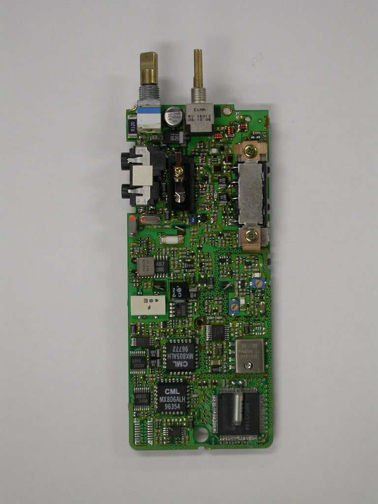
O78SC580
Jan 16, 2007UHF Portable Transceiver
Equipment Class
TNF - Licensed Non-Broadcast Transmitter Held to Face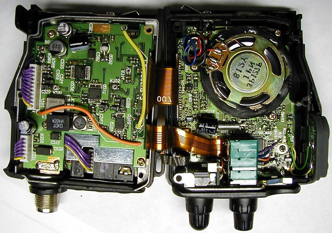
O78SCU99BL
Aug 02, 2001Hand Held Portable Transceiver
Equipment Class
TNF - Licensed Non-Broadcast Transmitter Held to Face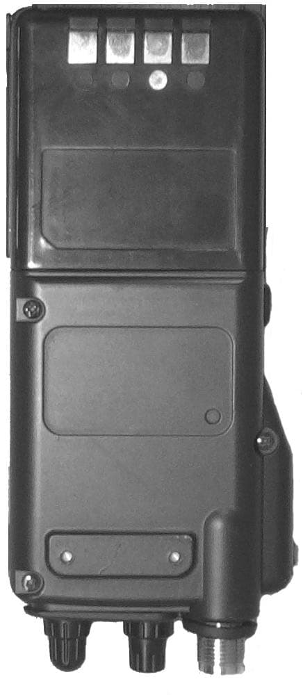
O78SCV99L
Jul 23, 2001VHF Portable Radio
Equipment Class
TNF - Licensed Non-Broadcast Transmitter Held to Face