O78SCV99LVHF Portable Radio
Smart Communications Ltd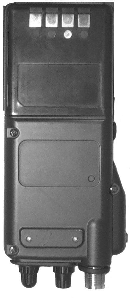
Click to zoom
Application Details
- Equipment Class
- TNF - Licensed Non-Broadcast Transmitter Held to Face
- Date of Grant
- Jul 23, 2001
- Application Purpose
- Original Equipment
- Date of Application
- Apr 28, 2001
- Equipment Note
- VHF Portable Radio
- Frequency Range
- 148.00000000 - 174.00000000
- Company
- Smart Communications Ltd
- Country
- Hong Kong
Documents & Files
Document Text
Text extracted from the exhibit documents filed with the FCC. Open a document above to read the original.
Users Manual
Smart Com Portable Transceiver SCV08 AND SCU08 INSTRUCTION MANUAL “think smart” 471 Ballard Drive Melbourne, FL 32935 Phone: 321-751-9047 Fax: 321-751-9074 www.smartcommusa.com Copyright 2001 Printed in China 2 SAFETY INFORMATION Your portable contains a low power transmitter. Then the Push-to-Talk button is pushed it sends out radio frequency signals. The device is authorized to operate at a duty factor not to exceed 50%. In august 1996, the Federal Communications Commission (FCC) adopted RF exposure guidelines with safety levels for hand-held devices USE only the supplied antenna. Unauthorized antennas, modifications, or attachments could damage the transceiver and may violate FCC regulations. CAUTION! NEVER hold the transceiver so that the antenna is very close to, or touching exposed parts of the body, especially the face or eyes, while transmitting. The transceiver will perform the best if the microphone is 2 to 4 in (5 to 10 cm) away from the lips and the transceiver is held in the vertical position. NEVER operate the transceiver with a headset or other audio accessories at high volume levels. NEVER short the battery terminals. NEVER press the PTT key unless transmitting. AVOID using or placing the transceiver in direct sunlight or in areas with temperatures below +14 F (-10 C) or above +122 F (+50 C). The basic operations, transmit, receive are guaranteed within the specified operating temperature range. DO NOT modify the transceiver for any reason SAFETY INFORMATION Your transceiver generates RF electromagnetic energy during transmit mode. This radio is designed for and classified as “Occupational Use Only” meaning it must be used during the course of employment by individuals aware of hazards, ant the techniques to minimize such hazards. This radio in NOT intended to be used by the General Public, and in an uncontrolled environment. This radio has been tested and complies with the FCC RF exposure limits for “Occupational Use Only”. The radio also complies with the following standards regarding to RF energy and electromagnetic energy levels and evaluation of such levels for exposure to humans: • FCC OET Bulletin 65 Edition 97-01 Supplement C, Evaluating Compliance with FCC Guidelines for Human Exposure to radio Frequency Electromagnetic Fields. • American national Standards Institute (C95.1-1992), IEEE Standard for Safety Levels with Respect to Human Exposure to radio Frequency Electromagnetic Fields, 3kHz to 3000 GHz. 3 • American National Standards Institute (C95.3-1992), IEEE Recommended Practice for the Measurement of Potentially Hazardous Electromagnetic Fields- RF and Microwave. TO ENSURE THAT YOUR EXPOSURE TO RF ELECTROMAGNETIC ENERGY IS WITHIN THE FCC ALLOWABLE LIMITS FOR OCCUPATIONAL USE, ALWAYS ADHERE TO THE FOLLOWING GUIDELINES: • Do not operate the radio without a proper antenna attached, as this may cause damage to the radio as well as cause the RF exposure to exceed the FCC limits. The proper antenn is supplied with the radio, do not use any other antenna not approved by the manufacturer. • Do not transmit more than 50% of the total radio use time. Transmitting more than the recommended 50% can cause FCC RF exposure requirements to be exceeded. The radio transmits when the PTT switch is pushed and the RED TX LED (indicator) is illuminated. • Always use SmartComm USA authorized accessories (antennas, batteries, speaker microphones, belt clips, etc). Use of any unauthorized accessories can cause the RF exposure to exceed the FCC limits. • Always keep the antenna at least 1cm (3/8 in) away from the body when transmitting to ensure that the FCC exposure limits are not exceeded. To ensure the best signal quality, hold the antenna at least 5 cm (2 in) from the mouth and slightly to one side. ELECTROMAGNETIC INTERFERENCE / COMPATIBILITY During transmissions the radio generates RF energy that can possibly cause interference with other systems or devices. To avoid such interference never operate the radio in RX or TX where signs are posted not to use transceivers. Do not use the radio in areas that are sensitive to electromagnetic radiation. Some examples of these locations are hospitals, blasting sites and airports. 4 INDEX Introduction........................................................................... Installation Battery Installation and Removal.................................... Antenna Installation and Removal................................... Transceiver Views................................................................... Transceiver Details.................................................................. Operation Turning Unit On........................................................ Channel Selection......................................... Mode Selection............................................ Tone Selection............................................. Busy Channel Lockout.................................... Transmitter Operation.................................................. Procedure................................................... High/Low Power Selection.............................. Time Out Timer............................................ Beep......................................................... Battery Information General Information.................................................... Maintenance........................................................................... Troubleshooting...................................................................... Specifications......................................................................... Warranty.............................................................................. PACKING LIST 1 – Transceiver Unit with Belt Clip 1 – Flexible, Helical-Wound Antenna 1 – 7.2V Rechargeable Ni-Cad Battery 1 – WCSC7 Battery Charger 1 – Instruction Manual IMPORTANT Please read all instructions thoroughly before operating the unit. 5 5 5 6 7 8 9 9 9 9 10 10 10 10 10 11 11 11 12 14 5 INTRODUCT…
Text truncated - open the document above for the full version.
Attestation Statements
June 18, 2001 Federal Communications Commission Reference: FCCID : O78SCV99L Reference 731 Confirmation Number: EA100798 Correspondence Reference Number:19536 Applicant:Smart Communications Ltd. Dear Sir or Madam: This equipment meets the requirements of FCC Rules as stated in Parts 90.203(e) and (g) as applicable. Programming of this product’s transmitter frequency can be ONLY accomplished by the manufacturer, a qualified service/maintenance personnel. This is controlled by controlling the distribution of the programming software and/or cloning cable hardware. The operator cannot program transmit or receive frequencies using the equipment’s external controls. Sincerely, Walter C Simciak Chief Engineer 5481 SAND LAKE DRIVE, MELBOURNE,FLORIDA • 32934 PHONE: 321-255-0329 • FAX: 321-255-0329
Cover Letter(s)
May 16, 2001 Federal Communications Commission Reference FCC ID:O78SCV99L For m 731 :EA100798 Dear Sir or Madam: In filling out the FCC Form 731, we inadvertently copied information from a wrong column concerning the power output of the above mentioned transceiver unit. (We were preparing both a UHF and a VHF unit at the time.) We are requesting that the application be modified to read 5 watts instead of 4 watts for the higher power output level. The unit frequency stability is +/- 2.5 ppm as tested, however, I had also copied the +/- 2.5 ppm as the FCC requirement from the UHF document. If this delays the application, please consider this a request to also change that to the required +/- 5.0 ppm. If this cannot be done, it is of little consequence as the radio will continue to be built to +/- 2,5 ppm stability. Sincerely, Walter C. Simciak Chief Engineer ADRad Communications, Inc. Melbourne, Florida 5481 SAND LAKE DRIVE, MELBOURNE,FLORIDA • 32934 PHONE: 321-255-0329 • FAX: 321-255-0329
External Photos
April 29, 2001 Federal Communications Commission Dear Sir or Madam: Contained within this document is are pictures of the exterior of the SCV32L transceiver. The unit will be sold under several model numbers, the SCV32L, The SCV99L, and the SCV08. The differences being in operating features such as number of channels stored in memory or front panel keypad/display or not. The unit tested was equipped with all features and keypad/display. This should represent the worst case situation for radiated performance. The FCC label is positioned as shown on the rear of the unit and the details are shown below. Where **** is replaced by SCV32L, SCV99L, or SCV08 dependent on the feature set in the microcontroller element. The radio is programmed either by cloning from another radio or by a PC. In the case of the PC programming, the application program required to talk to the radio is made available to only radio dealers or government agencies. 5481 SAND LAKE DRIVE, MELBOURNE,FLORIDA • 32934 PHONE: 321-255-0329 • FAX: 321-255-0329 FCC ID:SCV99L Canada: S/N Smart Communications, Limited Made in China (Possible Distributor Name) Model: **** UHF Transceiver – 2 –April 29, 2001 SCV32L/99L Top View SCV08 Top View Antenna Connector Programming Connector Ext. Microphone Connector Ext. Speaker Connector Tx Indicator Volume/Squelch Control Channel Selector – 3 –April 29, 2001 Push to Talk Keyboard FCC Label Area – 4 –April 29, 2001 SCV08 Front/Rear
ID Label/Location Info
April 29, 2001 Federal Communications Commission Dear Sir or Madam: Contained within this document is are pictures of the exterior of the SCV32L transceiver. The unit will be sold under several model numbers, the SCV32L, The SCV99L, and the SCV08. The differences being in operating features such as number of channels stored in memory or front panel keypad/display or not. The unit tested was equipped with all features and keypad/display. This should represent the worst case situation for radiated performance. The FCC label is positioned as shown on the rear of the unit and the details are shown below. Where **** is replaced by SCV32L, SCV99L, or SCV08 dependent on the feature set in the microcontroller element. The radio is programmed either by cloning from another radio or by a PC. In the case of the PC programming, the application program required to talk to the radio is made available to only radio dealers or government agencies. 5481 SAND LAKE DRIVE, MELBOURNE,FLORIDA • 32934 PHONE: 321-255-0329 • FAX: 321-255-0329 FCC ID:O78SCV99L Canada: S/N Smart Communications, Limited Made in China (Possible Distributor Name) Model: **** UHF Transceiver – 2 –April 29, 2001 SCV32L/99L Top View SCV08 Top View Antenna Connector Programming Connector Ext. Microphone Connector Ext. Speaker Connector Tx Indicator Volume/Squelch Control Channel Selector – 3 –April 29, 2001 Push to Talk Keyboard FCC Label Area – 4 –April 29, 2001 SCV08 Front/Rear
Internal Photos
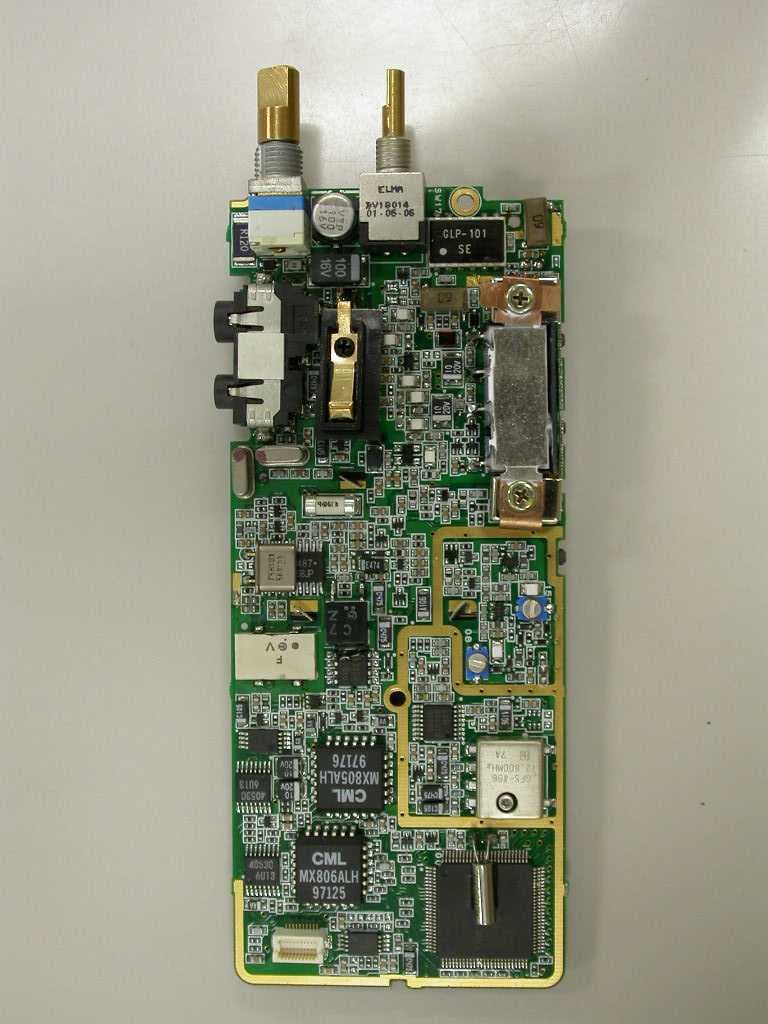
Sub-Board Top SideCPU Board FCC ID: O78SCV99L Interior Pictures Radio Front w/CPU BoardRear of Sub-Board RF Board with Shield in Place RF Board with Shield Removed
Operational Description
CIRCUIT DESCRIPTION GENERAL INFORMATION The SVC99L has three printed circuit boards; CPU board, Radio Frequency(RF)board, Audio Frequency (SUB)board. The CPU board contains the Microprocessor/Control section. The RF board contains the VCO/ Synthesizer section, Transmitter section and Receiver section. The SUB board contains the Transmitter Audio circuitry and the Receiver Audio circuitry. Circuitry is described in the following order: Microprocessor/Control Section, VCO/Synthesizer Section, Transmitter Section , Receiver Section and Battery Section. Refer to the Block Diagram and the Schematics. MICROPROCESSOR/CONTROL SECTION The microprocessor 0105 is constantly operating when the radio is turned ON. It is continuously monitoring the channel selector switch, The PTT line and other internal inputs such as the squelch detect, etc. When a change occurs, the microprocessor makes the appropriate response. The microprocessor is used for control, The Radio emits a beep on channel change and the synthesizer is loaded with the correct frequency information. The microprocessor runs off a 4.1 9 MHz oscillator which is composed of Xl 01, Cl 27, Cl 28, and Rl 28. When the radio is first turned on, the microprocessor reads the radio status from the EEPROM 0104. The microprocessor determines the receive frequency codes, then loads the synthesizer via its pins 17, 19 and 42. VCO/SYNTHESIZER SECTION This section consists of the Temperature-Compensated Crystal Oscillator (TCXO), Voltage Controlled Oscillator(VCO), Synthesizer and the Loop Filter. These circuits are found on the RF board. Tempe rat u r e-Compensated Crystal I Oscillator (TCXO) The reference oscillator is a temperature compensated crystal-controlled, Pierce type circuit. ft utilizes a logic gate within Q402 as a gain element. C407 is used to adjust the oscillator on frequency (6.4MHz) at room temperature (22'C). Temperature variations cause resistance changes in thermistor R410, which is on the base of 0404, thus varying the voltage applied to varactor 0403. This changes the impedance across crystal X401 in a manner complementary to the temperature drift characteristic of the crystal. In this way, the reference oscillator is held within the specified ±5 PPM from -30 to +60'C. Voltage-Cont r o II ed Os c i II at or s (VCO) Only one of the VCOs run at a time, which is controlled by the +SVTX (W402 Pin3) and Q429. When the FITT is pressed, +5VTX goes high (approx.5V) disabling the receive VCO and biases on Q429 to enable the transmitter VCO. Both the receive and transmitter VCOs are Colphs type oscillators. The receive VCO consists of C420-C423, L401-L403, and 0410-0412. This VCO oscillates at 21.4 MHz below the programmed receive frequency. The VCO's oscillating frequency is tuned by the varactors 0410 and Q41 1. The tuning voltage is supplied from the output of the Loop Filter. The output of the VCO is AC coupled (C424 and C425) to the synthesizer input buffer Q424 and the output buffer 0413 respectively. The transmitter VCO consists of C466-C469, L414-L416, and 0426-0428. This VCO oscillates on the programmed transmit frequency. The VCO's oscillating frequency is tuned by the varactors 0426 and Q427. The tuning voltage is supplied from the output of the Loop Filter The output of the VCO is AC coupled (C471 and C472) to the synthesizer input buffer Q424 and the output buffer Q430 respectively. The transmit voltage controlled oscillator is directly frequency-modulated and operates on the carrier frequency. In the receive mode, the transmit VCO is disabled and the receive VCO is enabled, producing the receive local oscillator signal at a frequency 21.4MHz below the incoming receive frequency. The synthesizer is tuned in 2.5OkHz or 5.OOkHz or 6.25kHz steps. Synthesizer The frequency synthesizer is a large scale monolithic synthesizer integrated circuit 0402. The synthesizer IC contains a dual modular prescaler, programmable divide-by-N counter, prescale control (swallow) counter, reference oscillator, reference divider, phase detector, charge pump and lock detector. Also, included in 0402 are shift registers and control circuits for frequency controls and general device control. RF output from the active VCO is buffered by Q424 and AC coupled to the synthesizer Q402 prescaler input at pin 8. The divide-by-N counter chain in Q402, consisting of the dual-modulus prescaler, swallow counter and programmable counter, divides the VCO signal down to a frequency very close to 2.5OkHz or 5.OOkHz or 6.25kHz, which is applied to the phase detector. The phase comparator compares the edges of this of this signal with that of the 2.5OkHz or 5.OOkHz or 6.25MHz reference signal from the reference divider and drives the external charge pump (0407 and Q406). The synthesizer unlock detector circuit prevents the operation of the transmitter, when the phase lock loop (PLL) is unlocked. The following discussion assumes the unit has been placed in the transmit mode. Q402 lock detector Pin 7 goes high when the PLL is locked. C413 charges through R416 cutting off Q406, then 0401 goes into cutoff thus applying a high to Pin 17 of the microprocessor QIOS. A software timing routing brings the RX/TX line low (Pin 15 of 01 05). With the RXITX line low, Q222B is cut off and Q221 B is biases on passing +SVTX (W402 Pin3) to saturate 0445B. After 0445 goes into saturation, ft biases on Q446 to pass switched battery B+ to the transmitter amplifier string which enables transmission. Should the PLL become unlocked, the lock detector at Q402 Pin7 will begin pulsing low. C413 quickly discharges, biasing on 0406. This, in turn, saturates 0401, presenting a low to the microprocessor. The microprocessor then changes the RXITX line to a high, thus signaling the other transistor switches to drive 0446 into cutoff, which disables transmission. Therefore, the transmitter remains disabled while the loop remains out of lock. Loop Filter The Loop Filter, a passive lead-lag filter consisting …
Text truncated - open the document above for the full version.
Parts List/Tune Up Info
ALIGNMENT/ADJUSTMENTS-SCV99L/32L/08 A.GENERAL For proper alignment, the unit should be programmed with the following channel and frequencies. Channel RX FrequencyTX FrequencyRX/TX ToneDTMF MHzMHzHz 1154.050154.050No ToneNone 2161.0475161.0475No ToneNone 3168.950168.950No ToneNone 4148.0475148.0025No ToneNone 5173.9925173.9575No ToneNone 6161.050161.00067 HzNone 7161.050161.000100 HzNone 8161.050161.000250 HzNone 9161.050161.000141 DCSNone 10162.050162.050012 DCSNone 11161.050169.900None1234 Make connection to the unit per Figure 5 (Equipment Test Set-Up) Below and Figure 6 (Test Adapter). For the location of the components in these procedures refer to RF and Sub board parts placement. B.SYNTHESIZER/TRANSMITTER VCO Check Note: VCO must be checked prior to transmitter and receiver alignment. 1. Connect the radio in accordance with Figure 5. 2. Place the Unit on channel 3 (168.95OMHz, RX; 168.99OMHz, TX). 3. Connect the voltmeter to TPI. Check to make sure that the voltmeter reading is between 3.90 V and 4.30 V when the unit is in the receive mode. 4. Operate the transmitter to make sure that the voltmeter reading at TPI is between 3.90 V and 4.30 V. NOTE: Refer to the following for typical values at TP1 ChannelReceive VTransmit V 12.10V2.30V 22.90V3.00V 33.95V4.00V 41.55V1.70V 54.70V4.70V Frequency Adjustment 1. Connect the Radio in accordance with Figure 5. 2. Place the Unit on channel 3 (168.95OMHz, RX; 168.99OMHz, TX). 3. Operate the transmitter and adjust C407 for a Frequency Counter reading within ± 5OHz of the programmed transmit frequency. 4. Place the Unit on channel 2 (161.0475MHz, RX; 161.0025MHz, TX). 5. Operate the transmitter and adjust C320 for a Frequency Counter reading 161.0025MHz ± 5Ohz TRANSMITTER ALIGNMENT Note: In order to obtain proper transmission output power, connect the Transceiver to the power supply with a cable that is rated to withstand a current of 2 Amps or greater. 1. Connect the Radio in accordance with Figure 6. 2. Place the Radio on the channel 2 (161.0475MHz, RX; 161.0025MHz, TX). 3. Place the Unit in HIGH POWER mode. 4. Turn R289 and R288 fully clockwise. 5. Operate the transmitter, using TA-SI, to make sure that the maximum RF output power reading on the wattmeter is 5.5 W or greater. 6. Adjust R289 (HI PWR ADJ) for a reading of 5.0 W ±0.1 W. Check to make sure that the transmit current is within 1000 - 1400 mA after the adjustment has been made. 7. Place the Unit in the LOW POWER mode. 8. Adjust R288 (LO PWR ADJ) for a reading of 1.0 W ±0.1 W. Check to make sure that the transmit current is within 500 - 700 mA after the adjustment has been made. 9. Operate the transmitter, using TA-SI, to make sure that the difference between the maximum and minimum transmitter output power reading is within 0.1 W 154.OOOMHz - 168.99OMHz range. 10, Place the Unit in HIGH POWER mode. 11. Operate the transmitter, using TA-SI, to make sure that the difference between the maximum and minimum transmitter output power reading is within 0.5 W in the 154.OOOMHz - 168.99OMHz range. MODULATION ADJUST 1. Connect the Radio in accordance with Figure 5. 2. Place the Radio on channel 2 (161.0475MHz, RX; 161.0025MHz, TX). 3. Apply a 1 kHz tone signal to Test Adapter's AF Input (Figure 6), which is the microphone impedance matching network. 4. Plug the Test Adapter into the external speaker/microphone jack. 5. Operate the transmitter, using TA-SI, and adjust the audio generator's output level for ±3kHz deviation on the Modulation Analyzer. Turn OFF the transmitter and note the audio generator's output level (TA- TP2). The level should be between 20 and 30 mV. 6. Increase the audio generator's output level by 20 dB. 7. Operate the transmitter, using TA-SI, and adjust the master deviation control R266 for ±4.OOkHz deviation on the Modulation Analyzer, if CTCSS or DCS is not to be employed. 8. To adjust CTCSS and DCS Deviation, perform step 1 though 7 above. Then set the FM liner detector audio bandwidth of <0.25Hz to >15,00OHz. Turn the de-emphasis function off. 9. Place the Radio on channel 9 (161.05OMHz, RX; 161.OOOMHz, TX). Set the audio generator output to OV operate the transmitter, using TA-SI and adjust the DCS balance control R291 to Ul-U2 is minimum on the Oscilloscope. 10. Place the Radio on channel 7 (161.05OMHz, RX; 161.OOOMHz, TX). Operate the transmitter using TA-SI, and adjust R705 to ±800 Hz deviation on Modulation Analyzer. 11. Place the Radio on channel 2 (161.0475MHz, RX; 161.0025MHz, TX) 12. To adjust DTMF deviation, perform steps I through 7 above. Set the audio generator output to 0V. Operate the transmitter, using TA-SI, and press the '8' key. Adjust the DTMF deviation on control R714 for ±3.0 kHz deviation on the Modulation Analyzer. RECEIVER 1. Connect the Radio in accordance with Figure 6. 2. Adjust the Squelch Control S299(SOL) to the fully counter-clockwise position (unit unsquelched) until the BUSY LED (Green) turns ON. 3. Place the Radio on the channel I (164.06OMHz, RX; 154.OOOMHz, TX). 4. Apply the RF generator signal with I kHz tone at 3 KHz deviation and adjust its RF output level to approximately -77 dBm. 5. Adjust L201 for the maximum audio level on the AC voltmeter (TA-TPI). 6. Connect the digital voltmeter to TP4; see Figure 9. 7. Preset the cores of L405 to the BOTTOM of the coil form and L406, L407, L408, L409 to the TOP of the coil form. 8. Adjust L405, L406, L407, L409, and L408 in this order to obtain the maximum voltmeter at TP4. Reduce the RF generator's level as necessary to maintain a mid scale reading on the voltmeter as the coils are adjusted. 9. Repeat step 8 until no further improvement can be made. 10. Check the 12dB SINAD sensitivity reading at both ends of the operating range of the Unit. The specification is 0.26 gV maximum.
Parts List/Tune Up Info
RF Board.... Sub Board Parts CPU Board Mechanical Parts
Test Report
Test Report... FCC ID: O78SCV99L Page 1 Test Report... FCC ID: O78SCV99L Assembled from Manufacture Measurements performed to EIA/TIA-603 and Measurements made at ADRad Communications, Inc. 29 April 2001 Test Report... FCC ID: O78SCV99L Page 2 Contents: 1. Specification Information 2. RF Power Output 3. Modulation Characteristics 4. Occupied Bandwidth 5. Spurious Emissions (Conducted) 6. Frequency Stability 7. Transient Frequency Characteristics 1.0 Specification Information Model Numbers:SCV99L, SCV32L, or SCV08 (Same RF and controller) Number of Channels:99, 32, or 8 channels dependent on model number. Frequency Range:148 to 174 MHz Channel Spacing:12.5 or 25 kHz Transmitter Power Output1 or 5 watt, user or programmer selectable. (A 1 dB) Battery Voltage:7.5 volts Current Drain:Tx...1800 mA @ 5 watts 800 mA @ 1 watt Rx... 160 mA @ 2 50 mW of Rx audio 50 mA @ standby Antenna Impedance:50 Ohms Frequency Stability:A 2.5 ppm Temperature Range:-30BC to +60BC Nominal Battery Voltage:7.5 VDC (6 cells NiCad or NMHy) Emission Designations:12.5 kHz Channel(2x2.5kHz deviation)+(2x3kHz) 11k0F3E 25.0 kHz Channel(2x5.0kHz deviation)+(2x3kHz) 16k0F3E for 3 kHz maximum modulation frequency All measurements made to TIA/EIA-603 procedures 2.0 RF Power Output At 5 watt Output Level DC Voltage @ -15%DC Voltage @ Nominal 7.5 VDCDC Voltage @+15% 4.5 Watts 5.5 Watts6.5 Watts At 1 watt Output Level DC Voltage @ -15%DC Voltage @ Nominal 7.5 VDCDC Voltage @+15% 0.95 Watts 1.00 Watts1.05 Watts Test Report... FCC ID: O78SCV99L Page 3 3.0 Modulation Characteristics Test Report... FCC ID: O78SCV99L Page 4 4.0 Occupied Bandwidth Plotted from data taken. 12.5 kHz BW Measurements -70 -60 -50 -40 -30 -20 -10 0 -20000-15000-10000-500005000100001500020000 Relative Frequency (Hz) Level (dB) Limit Mask D Measurements Plotted Data Occupied Bandwidth Unmodulated carrier set to 0 dB. 2500 Hz sinewave Input level 16 dB greater than required for 50% rated system deviation. Test Report... FCC ID: O78SCV99L Page 5 Plotted from data taken. 25 kHz BW Measurements -80 -70 -60 -50 -40 -30 -20 -10 0 -50000-45000-40000-35000-30000-25000-20000-15000-10000 -5000 0 5000 100001500020000250003000035000400004500050000 Relative Frequency (Hz) Level (dB) Limit Mask D Measurements Plotted Data Occupied Bandwidth Unmodulated carrier set to 0 dB. 2500 Hz sinewave Input level 16 dB greater than required for 50% rated system deviation. Test Report... FCC ID: O78SCV99L Page 6 5.0 Spurious Emissions (Conducted) 6.0 Frequency Stability FCC Limit is +/- 2.5 ppm. DC Voltage @ -15%DC Voltage @ Nominal 7.5 VDCDC Voltage @+15% +58 Hz (+0.47 ppm)+128 Hz (+0.8 ppm)+138 Hz (+0.86 ppm) Spurious with Five watt output, dBc ref to fundamental. All others >-20 dB below requirement Spurious with One watt output, dBc ref to fundamental Test Report... FCC ID: O78SCV99L Page 7 7.0 Transient Frequency Characteristics
Test Report
CD&TFCC ID: O78SCV32BL A. DEVICE UNDER TEST The device is a VHF Handheld Transceiver operating under Part 90 of the FCC rules. The transmit frequency range of operation is 150.050 MHz. to 174.050 MHz. B. MEASUREMENT PROCEDURE: TRANSMITTER SECTION CABINET RADIATED EMISSIONS Transmitter cabinet radiation field strength measurements were conducted according to the procedures set forth in ANSI C63.4 (1992). The device under test was terminated with a 50 ohm dummy load and placed on a rotating turntable 0.8 meters high, centered at 3 meters distant from the measurement antenna. The device was placed in the center of the turntable and tested in three major planes as shown in the photographs The device is powered by an internal 7.5V, NiCad rechargeable battery. The test was conducted with a fresh battery. A spare battery pack was on hand and was used after the first battery dropped to 85% capacity. For the purposes of testing, the device was locked in a constant transmit mode by holding the transmit key depressed with a rubber band. Testing was conducted at the low, mid and high ends of the operational range. The device was scanned from 30MHz. to 2GHz. and all emissions were noted. In this case, the only emissions detected were those harmonically related to the fundamental transmit frequency. RECEIVER SECTION RADIATED EMISSIONS Receiver radiation measurements were conducted according to the procedures set forth in ANSI C63.4 (1992). The device under test was placed on the center of turntable and terminated with the antenna supplied by the manufacturer. Testing was conducted with the device positioned in three major planes. The sample was tested the low, mid and high ends of its range. The squelch control was adjusted to allow sound from the speaker and the volume control was set to approximately one quarter rotation. The device was scanned from 30MHz. to 2GHz. and all emissions were noted. In this case, the only emissions detected were those harmonically related to the fundamental frequency of the first local oscillator. The manufacturer’s specifications indicated a second local oscillator running at 33.845 MHz., common to all channels. The fourth harmonic (135.380MHz.) of this oscillator was discernable at the antenna terminal (-68.22dBm.) when connected directly to the spectrum analyzer. However, none of the signals related to the second local oscillator were detectable under open field conditions. MEASUREMENTS The field strength measurements were taken using an HP8596E spectrum analyzer, an EMCO 3120 dipole set, an EMCO 3115 double ridge guide horn antenna and an Avantek UJ210 preamp. At each detected frequency of emission, the device was measured by rotating the turntable and adjusting the antenna height over a range of 1 to 4 meters to obtain the maximum output level. This procedure was performed with both horizontal and vertical antenna polarizations with the device placed in the positions shown in the photographs. The peak reading for each frequency was captured and recorded in the second column on the data sheet. C. FACILITY Radiated emissions testing for this device was conducted by Control Design & Testing, Inc. and performed on the Hyak Laboratories 3 meter open area test site located in Spotsylvania, VA. Receiver Testing, Vertical PlaneReceiver Testing, Horizontal, sides Receiver Testing, Horizontal, Front/Rear Transmitter Testing, Horizontal, SidesTransmitter Testing, Vertical Transmitter Testing, Horizontal, Front/Back
Contact Information
Applicant
George Kishikawa(CEO/President)
Technical Contact
ADRad Communications, IncWalter C Simciak
[email protected]321-255-0329
5481 Sand Lake Drive · Melbourne, Florida · United States
Non-Technical Contact
ADRad Communications, IncWalter C Simciak
[email protected]321-255-0329
Technical Specifications
| # | Rule Parts | Frequency Range | Power Output | Emission | Tolerance |
|---|---|---|---|---|---|
| 4 | 22,74,9 | 148 MHz - 174 MHz | 1 W | 16K0F3E | 2.5 ppm |
Other Applications from Smart Communications Ltd
O78SC280A
Dec 27, 2007VHF PORTABLE RADIO
Equipment Class
TNF - Licensed Non-Broadcast Transmitter Held to Face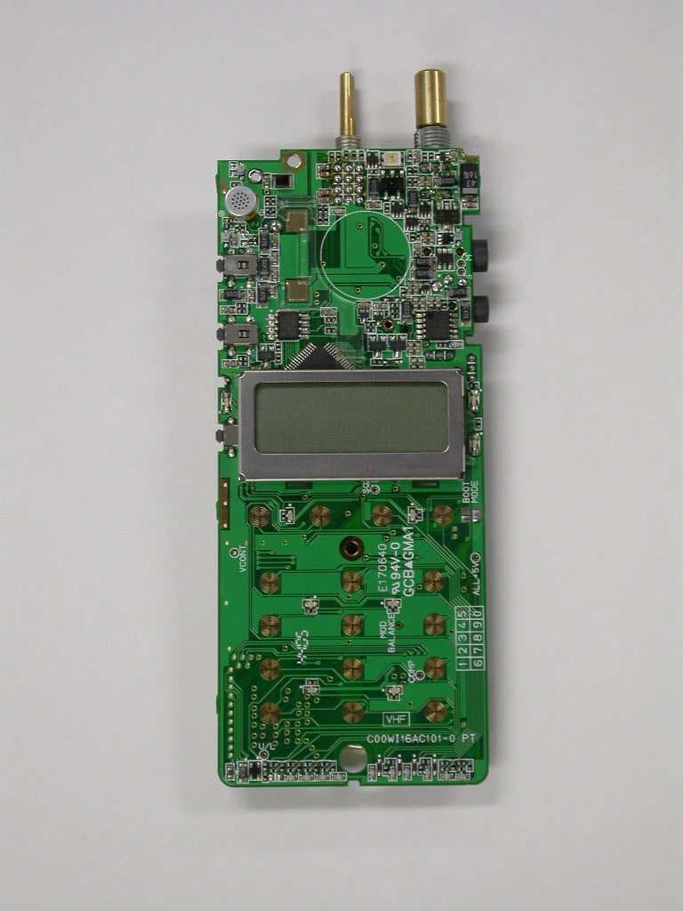
O78SC280
Jan 29, 2007VHF Portable Radio
Equipment Class
TNF - Licensed Non-Broadcast Transmitter Held to Face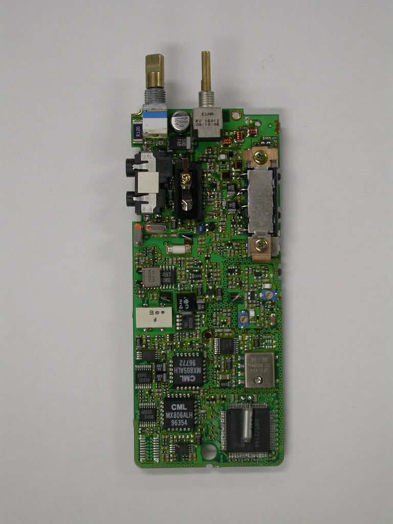
O78SC580
Jan 16, 2007UHF Portable Transceiver
Equipment Class
TNF - Licensed Non-Broadcast Transmitter Held to Face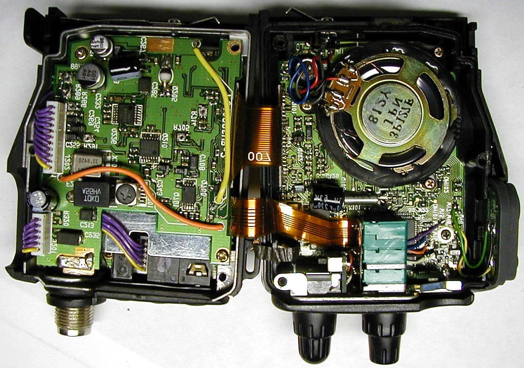
O78SCU99BL
Aug 02, 2001Hand Held Portable Transceiver
Equipment Class
TNF - Licensed Non-Broadcast Transmitter Held to Face