O7JAP-DS11Access Point 11Mbps
Global Sun Technology Inc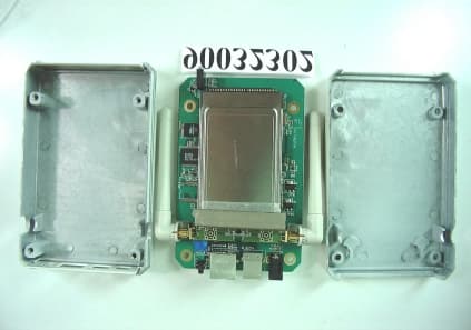
Click to zoom
Application Details
- Equipment Class
- DSS - Part 15 Spread Spectrum Transmitter
- Date of Grant
- May 02, 2001
- Application Purpose
- Original Equipment
- Date of Application
- May 02, 2001
- Equipment Note
- Access Point 11Mbps
- Frequency Range
- 2412.00000000 - 2462.00000000
- Company
- Global Sun Technology Inc
- Country
- Taiwan
Documents & Files
Document Text
Text extracted from the exhibit documents filed with the FCC. Open a document above to read the original.
Users Manual
G G L L 2 2 4 4 1 1 1 1 A A P P Access Point Version:1.0 Date:2000/10/04 1 FCC Information This equipment has been tested and found to comply with the limits for a Class A digital device pursuant to part 15 of the FCC Rules. These limits are designed to provide reasonable protection against harmful interference when the equipment is operated in a commercial environment. This equipment generates, uses, and can radiate radio frequency energy and, if not installed and used in accordance with the instruction manual, may cause harmful interference to radio communication. Operation of this equipment in residential area is likely to cause harmful interference in which case the user will be required to correct the interference at this own expense. The user should not modify or change this equipment without written approval of the company. Modification could make invalid any authority to use this equipment. It is unsafe to work under circumstances in which the RF exposure exceeds recommended amount. To prevent the situation happening, people who work with the antenna should be aware of the following rules: 1. Install the antenna so that a 20 cm distance can be kept from the antenna. 2. While installing the antenna in the location, please do not turn on the power of the wireless card. 3. While the device is working, please do not contact the antenna. This device complies with Part 15 FCC Rules. Operation is subject to the following two conditions: (1) This device may not cause harmful interference. (2) This device must accept any interference received including interference that may cause undesired operation." 2 Contents SECTION 1 ABOUT GL2411AP-0A ACCESS POINT ............................... 3 I NTRODUCTION ................................................................................................................................................ 3 1-1 F EATURES ................................................................................................................................................... 3 1-2 F IRMWARE FUNCTIONALITY ............................................................................................................. 3 1-3 A PPLICATIONS .......................................................................................................................................... 4 1-4 P RODUCT K IT ........................................................................................................................................... 4 SECTION 2 HARDWARE INSTALLATION ........................................................ 6 2-1 E QUIPMENT R EQUIREMENT .............................................................................................................. 6 2-2 GL2411AP-0A H ARDWARE I NSTALLATION ............................................................................ 6 2-3 S OFTWARE L IMITATION ....................................................................................................................... 6 SECTION 3 HOW TO CONFIGURE GL2411AP-0A ACCESS POINT .................................................................................................................................................................. 7 3-1 I NSTALLTION GL2411AP-0A AP BY USB CABLE F OR W INDOWS 98 ..................... 7 3-2 GL2411AP-0A AP U TILITY S ETUP .......................................................................................... 10 DFU (USB Configuration Utility) ..................................................................................................................... 10 SNMP Configuration Utility .............................................................................................................................. 12 3-3 GL2411AP-0A AP C ONFIGURATION U TILITY .................................................................... 14 DFU (USB Configuration Utility) ..................................................................................................................... 14 SNMP Configuration Utility .............................................................................................................................. 16 APPENDIX A NETWORK CONFIGURATION ............................................. 19 A-1 N ETWORK T OPOLOGY ...................................................................................................................... 19 Ad-Hoc Mode..................................................................................................................................................... 19 Infrastructure ..................................................................................................................................................... 19 A-2 R OAMING ................................................................................................................................................ 20 APPENDIX B SPECIFICATIONS .................................................................................. 21 APPENDIX C GLOSSARY ..................................................................................................... 22 3 Section 1 About GL2411AP-0A Access Point Introduction The GL2411AP-0A (11 Mbps WLAN Access Point) is a long-range, high performance LAN product, which provides Access Point services to a 2,4 GHz RF network and bridges to an Ethernet backbone. The design of this product is based on AT76C510 (bridge-on-a-chip) module, a highly integrated ASIC designed to combine legacy LANs with wireless LANs. AT76C510 performs all the necessary inter-networking and bridging functions. It receives data from both networks, stores them locally for further processing, installs and maintains connections and transmits the packets to the proper destination. Furthermore, AT76C510 interfaces three more modules, the Ethernet PHY, the wireless PHY and the RAM modules, for allowing compact system implementation and flexibility for supporting almost all the possible physical interfaces. 1-1 Feat…
Text truncated - open the document above for the full version.
Cover Letter(s)
Federal Communications Commission Authorization and Evaluation Division Confidentiality Request Pursuant to Sections 0.457 and 0.459 of the Commission’s Rules, the Applicant hereby requests confidential treatment of information accompanying this Application as outlined below: Schematics Block Diagram Parts Lists Operational Descriptions Internal Photos The above materials contain trade secrets and proprietary information not customarily released to the public. The public disclosure of these matters might be harmful to the Applicant and provide unjustified benefits to its competitors. The Applicant understands that pursuant to Rule 0.457, disclosure of this Application and all accompanying documentation will not be made before the date of the Grant for this application. Sincerely, Alan Lin Manager SUN COMMUNITCATIONS, INC. NO.13 Tung Yuan Rd., Jung Li Industrial Park Jung Li City, Tao Yuan Hsien, Taiwan, R.O.C Tel: 886-3-4617436 Fax: 886-3-4617441 FCC ID: O7JAP-DS.11
External Photos
Report No.: RF900323021Issued: April 4, 2001 ANNEX 2 PHOTOGRAPHS OF EUT Report No.: RF900323022Issued: April 4, 2001 Report No.: RF900323027Issued: April 4, 2001 Report No.: RF900323028Issued: April 4, 2001
ID Label/Location Info
FCC ID: O7JAP-DS11
ID Label/Location Info
FCC Label Position
Internal Photos
Report No.: RF900323023Issued: April 4, 2001 Report No.: RF900323024Issued: April 4, 2001 Report No.: RF900323025Issued: April 4, 2001 Report No.: RF900323026Issued: April 4, 2001
Test Report
FCC ID: O7JAP-DS.11 Report No.: RF90032302 23 Issued: April 4, 2001 4.2 RADIATED EMISSION MEASUREMENT 4.2.1 LIMITS OF RADIATED EMISSION MEASUREMENT Field strength limits are at the distance of 3 meters, emissions radiated outside of the specified bands, shall be according to the general radiated limits in 15.209 as following: Field Strength of Fundamental Frequencies (MHz) μV/meterdBμV/meter 30-8810040.0 88-21615043.5 216-96020046.0 Above 96050054.0 As shown in 15.35(b), for frequencies above 1000MHz, the field strength limits are based on average detector, however, the peak field strength of any emission shall not exceed the maximum permitted average limits, specified above by more than 20dB under any condition of modulation. LIMIT OF RADIATED EMISSION OF FCC PART 15, SUBPART B FOR FREQUENCY ABOVE 1000 MHz FREQUENCYClass A (at 10m)Class B (at 3m) (MHz)uV/mdBuV/m uV/mdBuV/m Above 100030049.550054.0 Note: 1 The lower limit shall apply at the transition frequencies. 2 Emission level (dBuV/m) = 20 log Emission level (uV/m). 3 All emanation from a class A/B digital device or system, including any network of conductors and apparatus connected thereto, shall not exceed the level of field strengths specified above. FCC ID: O7JAP-DS.11 Report No.: RF90032302 24 Issued: April 4, 2001 4.2.2 TEST INSTRUMENTS DESCRIPTION & MANUFACTURER MODEL NO.SERIAL NO. CALIBRATED UNTIL *HP Spectrum Analyzer8590L3544A01176April 18, 2001 *HP Preamplifier8447D2944A08485April 26, 2001 * HP Preamplifier8449B3008A01201Dec. 13, 2001 * ROHDE & SCHWARZ TEST RECEIVER ESMI 839013/007 839379/002 Jan. 25, 2002 SCHWARZBECK Tunable Dipole Antenna VHA 9103 UHA 9105 E101051 E101055 Nov. 23, 2001 * CHASE BILOG AntennaCBL6112A2221Aug. 4, 2001 * EMCO Turn Table10601115NA * SHOSHIN TowerAP-4701A6Y005NA * SoftwareAS61DNANA * ANRITSU RF SwitchesMP59BM35046Aug. 4, 2001 * TIMES RF cableLMR-600CABLE-ST5-01Aug. 4, 2001 * Antenna (Horn)BBHA9120-DD130July 10, 2001 Open Field Test SiteSite 5ADT-R05July 28, 2001 VCCI Site Registration No.Site 5R-1039NA NOTE: 1.The measurement uncertainty is less than +/- 3.0dB, which is calculated as per the NAMAS document NIS81. 2.The calibration interval of the above test instruments is 12 months. And the calibrations are traceable to NML/ROC and NIST/USA. 3.“*” = These equipments are used for the final measurement. FCC ID: O7JAP-DS.11 Report No.: RF90032302 25 Issued: April 4, 2001 4.2.3 TEST PROCEDURES 1. The EUT was placed on the turn table 0.8 meter above ground in 3 meter open area test site. 2. Set the resolution bandwidth to 120KHz in the test receiver and select Peak function to scan the frequency below 1 GHz. 3. Shift the interference-receiving antenna located in antenna tower upwards and downwards between 1 and 4 meters above ground and find out the local peak emission on frequency domain. 4. Locate the interference-receiving antenna at the position where the local peak reach the maximum emission. 5. Rotate the turn table and stop at the angle where the measurement device has maximum reading 6. Shift the interference-receiving antenna again to detect the maximum emission of the local peak 7. If the reading of the local peak under Peak function is lower than limit by 6dB, then Quasi Peak detection is not needed and this reading should be recorded. And if it is higher than Peak limit, then the test is fail. Others, switch the receiver to Quasi Peak function, set the resolution bandwidth to 100kHz and repeat the procedures C ~ F. If the reading is lower than limit, this reading should be recorded, otherwise, the test is fail. 8. Set the resolution and video bandwidth of the spectrum analyzer to 1MHz and repeat procedures C ~ F for frequency band from 1 GHz to 10 times carrier frequency. 9. If the reading for the local peak is lower than the Average limit, no further testing is needed in this local peak and this reading should be recorded. If it is higher than Average limit but lower than Peak limit, then set the resolution bandwidth to 1MHz and video bandwidth to 300Hz. Repeat procedures C ~ F. If the maximum reading is lower than Average limit, then this reading should be recorded. If it is higher, then the test is fail. Notes: 1.The frequency range of verification is either from 30 MHz to 1GHz or from 30 MHz up to 10 times carrier frequency of EUT (whichever is the highest frequency range). 2.The resolution bandwidth and video bandwidth of test receiver/spectrum analyzer is 120kHz for frequency below 1GHz. 3.The resolution bandwidth of test receiver/spectrum analyzer is 1 MHz and the video bandwidth is 300 Hz for frequency above 1GHz. FCC ID: O7JAP-DS.11 Report No.: RF90032302 26 Issued: April 4, 2001 4.2.4 TEST SETUP For the actual test configuration, please refer to the related Item in this test report (Photographs of the Test Configuration). FCC ID: O7JAP-DS.11 Report No.: RF90032302 27 Issued: April 4, 2001 4.2.5 TEST RESULTS Digital Portion EUTAccess Point 11MbpsModelGL2411AP-1 Te s t M o d e1Detector FunctionQuasi-Peak ChannelChannel 1 Frequency Range30-1000 MHzTest Distance3M Environmental Conditions 24°C, 60%RHTe s t e d B ySteven Lu ANTENNA POLARITY: VERTICAL Frequency (MHz) Correction Factor (dB) Reading Va l u e (dBuV) Emission Level (dBuV/m) Limit (dBuV/m) Margin (dB) Antenna Height (cm) Table Angle (Degree) 132.03 13.5143.71 30.243.5-13.3115274 176.0715.6247.9232.3 43.5 -11.2115308 440.017.8038.9031.1 46.0 -14.9189274 572.046.0142.8936.9 46.0 -9.1100107 748.013.9849.4945.546.0-0.5107192 836.013.3336.2132.946.0-13.1149221 ANTENNA POLARITY: HORIZONTAL Frequency (MHz) Correction Factor (dB) Reading Va l u e (dBuV) Emission Level (dBuV/m) Limit (dBuV/m) Margin (dB) Antenna Height (cm) Table Angle (Degree) 132.0413.5145.26 31.843.5-11.8100228 176.0415.6240.7125.143.5-18.4162259 440.017.8035.4127.646.0-18.4198303 572.016.0143.7737.846.0-8.2100129 748.013.9845.5141.546.0-4.5115363 836.113.3337.9134.646.0-11.4104192 Notes: 1 Emission level (dBuV/m) = Reading value (dBuV).-Correction Factor (dB)…
Text truncated - open the document above for the full version.
Test Report
FCC ID: O7JAP-DS.11 Report No.: RF90032302 1 Issued: April 4, 2001 ANNEX 1 PROCESSING GAIN OF DIRECT SEQUENCE SPREAD SPECTRUM MEASUREMENT 1. 1.1. 1. LIMITS OF PROCESSING GAIN OF A DIRECT SEQUENCE SPREAD SPECTRUM MEASUREMENT The limit of processing gain is 10dB 1.1 TEST INSTRUMENTS & SUPPORT UNIT Description & ManufacturerModel No.Serial No. Anritsu Spectrum Analyzer, 9kHz to 30GHz MS2667CM10281 Anritsu Signal Generator, 10kHz to 20GHz 68247B984703 Hewlett Packard Power Meter,HP438A2743A04416 Hewlett Packard Power Sensor, -30 to 20dBm 8485A2942A08387 Hewlett Packard Step Attenuator, 10dB steps HP8496B3247A18505 Mini-Circuits Power SplitterZN2PD-9GNA DELL Laptop ComputerInspiron 5000eNA Campaq Laptop ComputerPPX99125 FCC ID: O7JAP-DS.11 Report No.: RF90032302 2 Issued: April 4, 2001 1.2 METHOD OF MEASUREMENT The processing gain may be measured using the CW jamming margin method. Section 4.7.4 shows the test configuration. The test consists of stepping a signal generator in 50 kHz increments across the passband of the system. At each point, the generator level required to produce the recommended Bit Error Rate (BER) is recorded. This level is jammer level. The output power of the transmitting unit is measured at the same point. The jammer to Signal (J/S) ratio is then calculated. Discard the worst 20% of the J/S data points. The lowest remaining J/S ratio is used when calculating the Process Gain. The reference PER is specified as 8%. The corresponding Es/No (signal to noise ratio per symbol) is 16.4 dB. The curve is attached as below. This value and the measured J/S ratio are used in the following equation to calculate the Process Gain (Gp) of the system. Where: (S/N) o : Signal to noise ratio for the chosen BER. Gp = (S/N) o +Mj+Lsys FCC ID: O7JAP-DS.11 Report No.: RF90032302 3 Issued: April 4, 2001 Mj : Maximum jammer to Signal Ratio recorded at the detected BER. Lsys : System losses . For the purpose of this processing gain calculation, we assume Lsys at its minimum value of 2 dB. TEST SETUP 7 NOTEBOOK EUT ANRITSU SIGNAL GENERATOR EUT NOTEBOOK PWR SENSOR 8485A Power meter HP 438A Mini-Circuits 15542 ZNZPD-9G HP8496D STEP ATTN 110dB (10dB steps) Matched Cables RECEIVER Transmitter FCC ID: O7JAP-DS.11 Report No.: RF90032302 4 Issued: April 4, 2001 1.3 TEST PROCEDURES Obtain the simplex link shown. Perform all independent instrumentation calibrations prior to this procedure. Set operating power levels using fixed and variable attenuators in system to meet the following objectives: Signal Power at receiver approximately –55dBm (above thermal sensitivity such that thermal noise does not cause bit errors. Signal Power at power meter between –20 and –30dBm for optimal linearity. Use spectrum analyzer to monitor test. Ensure that CW Jammer generator RF output is disabled and measure the power at the power meter port using the power meter. This is the relative signal power, Sr. Disable Transmitter, and set CW Jammer generator RF output frequency equal to the carrier frequency and enable generator output. Set reference CW Jammer power level at power meter port 8.4dB below Sr (minimum J/S, or 10dB processing gain reference level). Note the power level setting on the generator, this is the reference CW Jammer power setting, Jr. Disable CW Jammer, re-establish link. PER test should be operating essentially error -free. Enable CW Jammer at the reference power level and verify that the PER test indicates a PER of less than 8%. Alternatively, adjust the CW Jammer level to that which causes 8% PER and verify that the S/J is less than 8.4dB. Repeat step 7 for uniform steps in frequency increments of 50 kHz across the receiver passband with the CW Jammer. In this case the receiver passband is +/- 8.5 MHz. The numerical data associated with the following radio channel is tabulated and presented for Channel 1,6, and 11. Note:Since the jamming signal will be blocked by the IF filter if the jamming frequency is far form the center of the carrier frequency. So, only those frequencies around carrier frequency are shown here. FCC ID: O7JAP-DS.11 Report No.: RF90032302 5 Issued: April 4, 2001 1.4 EUT OPERATING CONDITION The software provided by client to set the EUT to transmit at lowest, middle and highest channel. 1.5 TEST RESULTS EUTAccess Point 11MbpsModelGL2411AP-1 Environmental Conditions20°C, 60%RHTe s t e d B ySteven Lu Although the theoretical processing gain is lower than 10 dB, but the CCK coding provides an extra coding gain of 2.2dB. 11Mbps CHANNEL 1 Processing Gain FrequencyGp(S/N)Mj = J/SLsys (GHz)(dB)(dB)(dB)(dB) 2.4080013.416.4-4.01 2.4080513.316.4-4.11 2.4081012.916.4-4.51 2.4081513.116.4-4.31 2.4082013.516.4-3.91 2.4082513.316.4-4.11 2.4083012.516.4-4.91 2.4083512.616.4-4.81 2.4084012.816.4-4.61 2.4084512.716.4-4.71 2.4085012.816.4-4.61 2.4085512.616.4-4.81 2.4086012.416.4-5.01 2.4086512.016.4-5.41 2.4087012.316.4-5.11 2.4087512.016.4-5.41 2.4088012.616.4-4.81 2.4088512.016.4-5.41 2.4089012.516.4-4.91 2.4089512.316.4-5.11 2.4090012.016.4-5.41 2.4095011.816.4-5.61 FCC ID: O7JAP-DS.11 Report No.: RF90032302 6 Issued: April 4, 2001 11Mbps CHANNEL 1 Processing Gain FrequencyGp(S/N)Mj = J/SLsys (GHz)(dB)(dB)(dB)(dB) 2.4095511.716.4-5.71 2.4096011.516.4-5.91 2.4096511.316.4-6.11 2.4097011.416.4-6.01 2.4097511.016.4-6.41 2.4098011.216.4-6.21 2.4098511.416.4-6.01 2.4099011.516.4-5.91 2.4099510.516.4-6.91 2.4100010.416.4-7.01 2.4100511.416.4-6.01 2.4101010.816.4-6.61 2.4101511.616.4-5.81 2.4102011.016.4-6.41 2.4102510.916.4-6.51 2.4103010.816.4-6.61 2.4103511.816.4-5.61 2.4104011.016.4-6.41 2.4104511.516.4-5.91 2.4105011.216.4-6.21 2.4105512.916.4-4.51 2.4106012.916.4-4.51 2.4106512.816.4-4.61 2.4107011.516.4-5.91 2.4107511.616.4-5.81 2.4108011.016.4-6.41 2.4108511.816.4-5.61 2.4109011.416.4-6.01 2.4109511.816.4-5.61 2.4110011.616.4-5.81 2.4110511.016.4-6.41 2.4111011.616.4-5.81 2.4111511.116.4-6.31 2.4112011.216.4-6.21 FCC ID: O7JAP-DS.11 Report No.: RF90032302 7 Issued: April 4, 2001 11Mbps CHANNEL 1 …
Text truncated - open the document above for the full version.
Test Report
FCC ID: O7JAP-DS.11 Report No.: RF90032302 41 Issued: April 4, 2001 4.4 MAXIMUM PEAK OUTPUT POWER 4.4.1 LIMITS OF MAXIMUM PEAK OUTPUT POWER MEASUREMENT The Limit of Maximum Peak Output Power Measurement is 30dBm. 4.4.2 INSTRUMENTS Description & ManufacturerModel No.Serial No.Calibrated Until ROHDE & SCHWARZ TEST RECEIVER ESMI839379/002Aug. 04, 2001 HP ATTENUATOR8496B3247A18505Cal. on use HP PLOTTER7475A2641V27755N/A Notes: 1.The measurement uncertainty is less than +/- 2.6dB, which is calculated as per the NAMAS document NIS81. 2.The calibration interval of the above test instruments is 12 months. And the calibrations are traceable to NML/ROC and NIST/USA. FCC ID: O7JAP-DS.11 Report No.: RF90032302 42 Issued: April 4, 2001 4.4.3 TEST PROCEDURES 1. The transmitter output was connected to the spectrum analyzer through an attenuator. 2. The center frequency of the spectrum analyzer is set to the fundamental frequency and using 3 MHz RBW and 3 MHz VBW. 3. The span of the spectrum analyzer should be larger than 6dB BandWidth plus 10MHz. 4. Use Peak Search to read the peak power after Maximum Hold function is activated. 5. Shift the marker to +/- 3MHz and +/-6MHz, and record the reading. 6. The Maximum Peak Output Power is the linear summation of the 5 readings in (4) and (5). Note: This measurement is the total power of 15MHz bandwidth which is far more wider than 6dB bandwidth. 4.4.4 TEST SETUP For the actual test configuration, please refer to the related Item – Photographs of the Test Configuration. 4.4.5 EUT OPERATING CONDITION The software provided by client enabled the EUT to transmit and receive data at lowest, middle and highest channel frequencies individually. EUT SPECTRUM ANALYZER Attenuator FCC ID: O7JAP-DS.11 Report No.: RF90032302 43 Issued: April 4, 2001 4.4.6 TEST RESULTS Output Power Into Antenna: EUTAccess Point 11MbpsModelGL2411AP-1 Environmental Conditions 24°C, 60%RHTe s t e d B ySteven Lu CHANNEL CHANNEL FREQUENCY (MHz) PEAK POWER OUTPUT (dBm) PEAK POWER LIMIT (dBm) PASS/FAI L 1241217.4930PASS 6243717.0630PASS 11246217.4130PASS FCC ID: O7JAP-DS.11 Report No.: RF90032302 44 Issued: April 4, 2001 4.5 POWER SPECTRAL DENSITY MEASUREMENT 4.5.1 LIMITS OF POWER SPECTRAL DENSITY MEASUREMENT The Limit of Power Spectral Density Measurement is 8dBm. 4.5.2 TEST INSTRUMENTS Description & ManufacturerModel No.Serial No.Calibrated Until ROHDE & SCHWARZ TEST RECEIVER ESMI839379/002Aug. 04, 2001 HP ATTENUATOR8496B3247A18505Cal. on use HP PLOTTER7475A2641V27755N/A Notes: 1.The measurement uncertainty is less than +/- 2.6dB, which is calculated as per the NAMAS document NIS81. 2.The calibration interval of the above test instruments is 12 months. And the calibrations are traceable to NML/ROC and NIST/USA. FCC ID: O7JAP-DS.11 Report No.: RF90032302 45 Issued: April 4, 2001 4.5.3 TEST PROCEDURE The transmitter output was connected to the spectrum analyzer through an attenuator, the bandwidth of the fundamental frequency was measured with the spectrum analyzer using 3 kHz RBW and 30 kHz VBW, set sweep time=span/3kHz. The power spectral density was measured and recorded. The sweep time is allowed to be longer than span/3KHz for a full response of the mixer in the spectrum analyzer. 4.5.4 TEST SETUP For the actual test configuration, please refer to the related Item – Photographs of the Test Configuration. 4.5.5 EUT OPERATING CONDITION The software provided by client enabled the EUT to transmit and receive data at lowest, middle and highest channel frequencies individually. EUT SPECTRUM ANALYZER Attenuator FCC ID: O7JAP-DS.11 Report No.: RF90032302 46 Issued: April 4, 2001 4.5.6 TEST RESULTS EUTAccess Point 11MbpsModelGL2411AP-1 Environmental Conditions 24°C, 60%RHTe s t e d B ySteven Lu CHANNEL NUMBER CHANNEL FREQUENCY (MHz ) RF POWER LEVEL IN 3 KHz BW (dBm) MAXIMUM LIMIT (dBm) PASS/FAI L 12412-12.798PASS 62437-13.028PASS 112462-12.748PASS FCC ID: O7JAP-DS.11 Report No.: RF90032302 47 Issued: April 4, 2001 CH1 FCC ID: O7JAP-DS.11 Report No.: RF90032302 48 Issued: April 4, 2001 CH6 FCC ID: O7JAP-DS.11 Report No.: RF90032302 49 Issued: April 4, 2001 CH11 FCC ID: O7JAP-DS.11 Report No.: RF90032302 50 Issued: April 4, 2001 4.6 BAND EDGES MEASUREMENT 4.6.1 LIMITS OF BAND EDGES MEASUREMENT Below –20dB of the highest emission level of operating band (in 100KHz RB). 4.6.2 TEST INSTRUMENTS Description & ManufacturerModel No.Serial No.Calibrated Until ROHDE & SCHWARZ TEST RECEIVER ESMI 848926/005 846839/018 Dec 03, 2001 HP ATTENUATOR8496B3247A18505Cal. on use HP PLOTTER7475A2641V27755N/A Notes: 1.The measurement uncertainty is less than +/- 2.6dB, which is calculated as per the NAMAS document NIS81. 2.The calibration interval of the above test instruments is 12 months. And the calibrations are traceable to NML/ROC and NIST/USA. 4.6.3 TEST PROCEDURE The transmitter output was connected to the spectrum analyzer via a low lose cable. Set both RBW and VBW of spectrum analyzer to 100 kHz with suitable frequency span including 100 kHz bandwidth from band edge. The band edges was measured and recorded. FCC ID: O7JAP-DS.11 Report No.: RF90032302 51 Issued: April 4, 2001 4.6.4 EUT OPERATING CONDITION The software provided by client enabled the EUT to transmit and receive data at lowest, middle and highest channel frequencies individually. 4.6.5 TEST RESULTS The spectrum plots are attached below. D2 line indicates the highest level, D1 line indicates the 20dB offset below D2. It shows compliance with the requirement in part 15.247(C). FCC ID: O7JAP-DS.11 Report No.: RF90032302 52 Issued: April 4, 2001 4.6.6 NOTE ON BAND EDGE EMISSION The band edge emission plot on page 43 shows 49.11dB delta between carrier maximum power and local maximum emission in restrict band (2.484GHz). The emission of carrier strength list in table of page 24 is 95.0dBμV/m, so the maximum field strength in restrict band is 95.0-49.11=45.89 dBμV/m which is under 54 dBμV/m limit. FCC ID: O7JAP-DS.11 Report No.: RF90032302 53 Issued: April 4,…
Text truncated - open the document above for the full version.
Test Setup Photos
FCC ID: O7JAP-DS.11 Report No.: RF90032302 56 Issued: April 4, 2001 5 PHOTOGRAPHS OF THE TEST CONFIGURATION CONDUCTED EMISSION TEST FCC ID: O7JAP-DS.11 Report No.: RF90032302 57 Issued: April 4, 2001 RADIATED EMISSION TEST
Contact Information
Applicant
Alex Wu(CTO)
Test Firm
Bureau Veritas CPS (H.K.) Ltd. Taoyuan BranchTommy Wu
Technical Specifications
| # | Rule Parts | Frequency Range | Power Output |
|---|---|---|---|
| 1 | 15C | 2.41 GHz - 2.46 GHz | 56.00 mW |
Other Applications from Global Sun Technology Inc

O7J-WLUD2554-17A
Apr 17, 2005802.11 a+g Wireless USB Dongle
Equipment Class
NII - Unlicensed National Information Infrastructure TX
O7J-WL012454-25M
Oct 24, 2004802.11g Wireless LAN Network Adapter
Equipment Class
DTS - Digital Transmission System
O7J-WLUD2454-13I
Sep 30, 2004802.11g Wireless USB Dongle
Equipment Class
DTS - Digital Transmission System
O7J-WLMP2454-1A3
Sep 25, 2004802.11g Wireless mini-PCI Module
Equipment Class
DTS - Digital Transmission System
O7J-WLRT2454NMA40
Jul 29, 2004AT&T Plug&Share 54Mbps Wireless Router
Equipment Class
DTS - Digital Transmission System