O9EQ2438F-MTRI MODE CDMA WIRELESS MODULE KIT
Sierra Wireless, ULC
Click to zoom
Application Details
- Equipment Class
- PCB - PCS Licensed Transmitter
- Date of Grant
- Jun 05, 2005
- Application Purpose
- Original Equipment
- Date of Application
- Jun 05, 2005
- Equipment Note
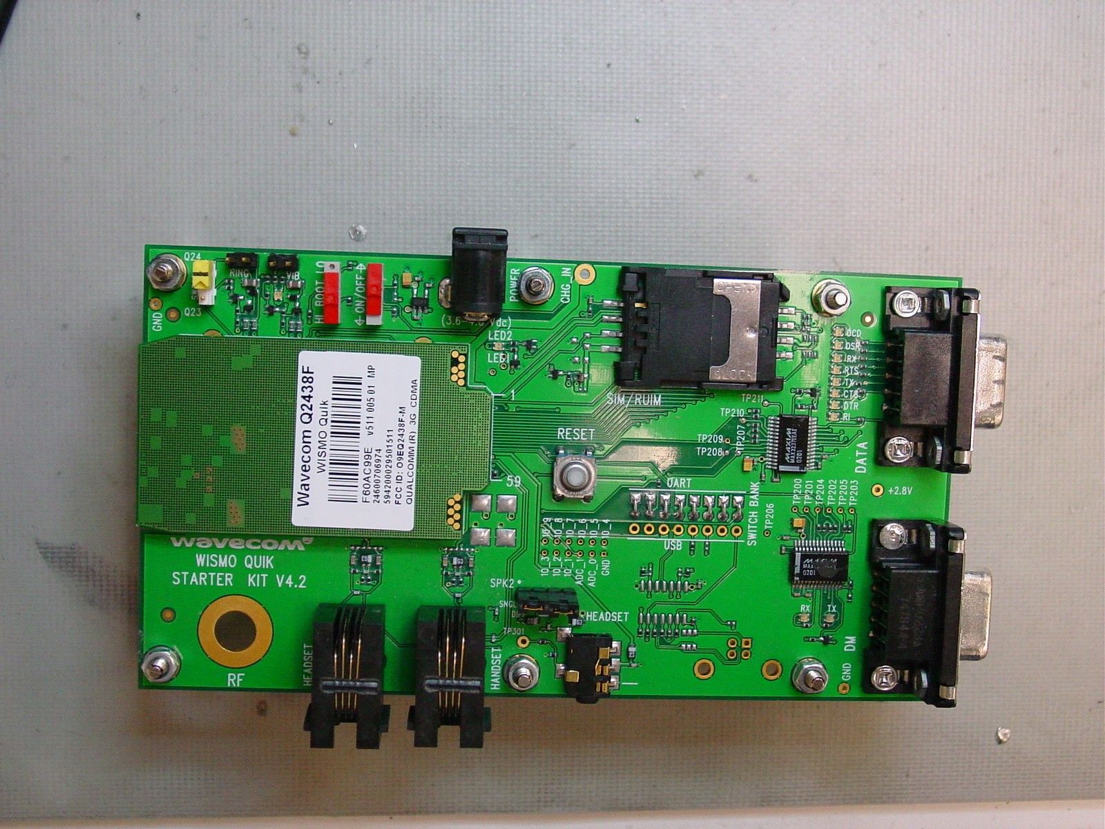
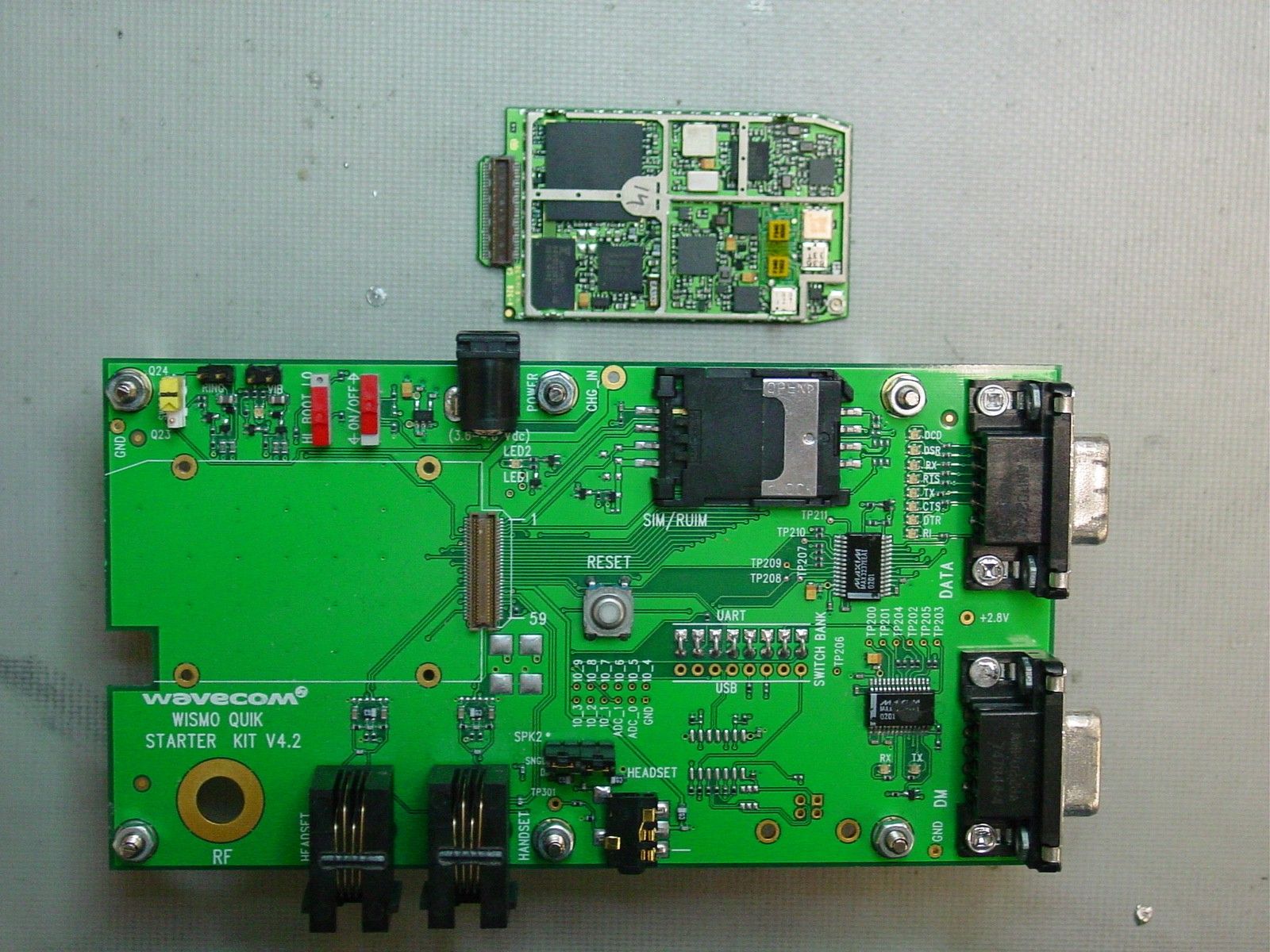
- TRI MODE CDMA WIRELESS MODULE KIT
- Frequency Range
- 824.04000000 - 848.97000000
- Company
- Sierra Wireless, ULC
- Country
- Canada
Documents & Files
Document Text
Text extracted from the exhibit documents filed with the FCC. Open a document above to read the original.
Users Manual
Confidential © Page: 1 / 18 This document is the sole and exclusive property of WAVECOM. Not to be distributed or divulged without prior written agreement. Ce document est la propriété exclusive de WAVECOM. Il ne peut être communiqué ou divulgué à des tiers sans son autorisation préalable. Q2438F-M/Starter Kit V2 User Guide Reference: WI_HWD_SK_UGD_002 Level : 003 Date: June 1, 2005 WM_HWD_SK_UGD_002 - 002 6/1/2005 Confidential © Page: 2 / 18 This document is the sole and exclusive property of WAVECOM. Not to be distributed or divulged without prior written agreement. Ce document est la propriété exclusive de WAVECOM. Il ne peut être communiqué ou divulgué à des tiers sans son autorisation préalable. Document Information Level Date History of the evolution Writer 001 23/9/2002 First draft RNixon 002 24/9/2002 Mechanical drawings update RNixon 003 27/6/2003 Add PDF Schematic RNixon Name Function Date Signature Written by Russ Nixon Hardware Engineer 23/9/02 Checked by Approved by WM_HWD_SK_UGD_002 - 002 6/1/2005 Confidential © Page: 3 / 18 This document is the sole and exclusive property of WAVECOM. Not to be distributed or divulged without prior written agreement. Ce document est la propriété exclusive de WAVECOM. Il ne peut être communiqué ou divulgué à des tiers sans son autorisation préalable. Contents 1 OVERVIEW............................................................................................................................................... 4 2 PRODUCT DESCRIPTION ..................................................................................................................... 5 3 DESCRIPTION OF THE INTERFACES ............................................................................................... 5 3.1 POWER.................................................................................................................................................. 5 3.2 COMPUTER........................................................................................................................................... 6 3.2.1 DATA ........................................................................................................................................... 6 3.2.2 DM ............................................................................................................................................... 6 3.3 SWITCHES AND JUMPERS...................................................................................................................... 6 3.3.1 ON/OFF Switch ........................................................................................................................... 6 3.3.2 BOOT Switch ............................................................................................................................... 7 3.3.3 RESET Switch .............................................................................................................................. 7 3.3.4 SNGL/DIFF Jumper .................................................................................................................... 7 3.4 AUDIO.................................................................................................................................................. 7 3.4.1 Handset ........................................................................................................................................ 7 3.4.2 Headset ........................................................................................................................................ 7 3.5 RF ........................................................................................................................................................ 8 3.5.2 FCC and Industry Canada Regulatory compliance ..................................................................... 9 3.6 SIM SOCKET...................................................................................................................................... 10 3.7 ADDITIONAL INTERFACES................................................................................................................... 10 3.7.1 Vibrator...................................................................................................................................... 10 3.7.2 Ringer ........................................................................................................................................ 11 3.7.3 GPIO.......................................................................................................................................... 11 3.7.4 Keypad ....................................................................................................................................... 11 3.7.5 JTAG .......................................................................................................................................... 11 3.8 LED FUNCTION.................................................................................................................................. 12 3.8.1 LED1.......................................................................................................................................... 12 3.8.2 LED2.......................................................................................................................................... 12 4 START-UP ............................................................................................................................................... 12 4.1 CONNECTIONS.................................................................................................................................... 12 4.2 CONFIGURATION................................................................................................................................. 13 4.2.1 Computer ................................................................................................................................... 13 4.2.2 Power Supply ......…
Text truncated - open the document above for the full version.
ID Label/Location Info
Q2438F-M FCC ID label
ID Label/Location Info
Q2438F-M FCC ID label Location
Operational Description
Wavecom Wismo Quik Q2438F-M Module RF Circuitry Description: Frequency Tuning This product has factory preset frequency adjustment. There is no frequency field adjustment for this product. In the field, frequency is locked to the base station and controlled by the VCTCXO adjustments to offset any possible error. Limiting Power Each mobile is individually calibrated at the factory to ensure a minimum MAX power of 23.0dBm (Cellular and PCS CDMA) and MIN power of –50dBm by employing proper frequency and temperature compensation schemes for both the RX and TX automatic gain control (AGC) amplifier. Suppression of Spurious Radiations Spurious and harmonic suppression is achieved by proper design with various filters and sufficient use of metallic shields. Rigorous testing at the factory ensures continuous compliance. Frequency Stability A voltage controlled temperature compensated crystal oscillator (VCTCXO) is utilized as a frequency reference for all of the transceiver local oscillators. This crystal oscillator is specified to a frequency stability of +/- 2.5ppm. The synthesizer lock status is constantly monitored by the microprocessor and transmission is disabled whenever an out of lock condition is detected. The mobile is locked to the base station and makes necessary frequency adjustments on the VCTCXO to correct and frequency errors between the mobile and the base station. Limiting Modulation The audio input is sampled, digitally limited, and then filtered to an amplitude and frequency limit the signal applied to the modulator. The device supports IS-2000 for CDMA operation, and IS-98 for AMPS operation. The device has an operating temperature of –30 o C to +60 o C. The functions include a compandor, PLL lock detector, filtering of received data, audio signal filtering for signals.
Parts List/Tune Up Info
Wavecom Wismo Quik Q2438F-M Module RF Circuitry Description: Frequency Tuning This product has factory preset frequency adjustment. There is no frequency field adjustment for this product. In the field, frequency is locked to the base station and controlled by the VCTCXO adjustments to offset any possible error. Limiting Power Each mobile is individually calibrated at the factory to ensure a minimum MAX power of 23.0dBm (Cellular and PCS CDMA) and MIN power of –50dBm by employing proper frequency and temperature compensation schemes for both the RX and TX automatic gain control (AGC) amplifier. Suppression of Spurious Radiations Spurious and harmonic suppression is achieved by proper design with various filters and sufficient use of metallic shields. Rigorous testing at the factory ensures continuous compliance. Frequency Stability A voltage controlled temperature compensated crystal oscillator (VCTCXO) is utilized as a frequency reference for all of the transceiver local oscillators. This crystal oscillator is specified to a frequency stability of +/- 2.5ppm. The synthesizer lock status is constantly monitored by the microprocessor and transmission is disabled whenever an out of lock condition is detected. The mobile is locked to the base station and makes necessary frequency adjustments on the VCTCXO to correct and frequency errors between the mobile and the base station. Limiting Modulation The audio input is sampled, digitally limited, and then filtered to an amplitude and frequency limit the signal applied to the modulator. The device supports IS-2000 for CDMA operation, and IS-98 for AMPS operation. The device has an operating temperature of –30 o C to +60 o C. The functions include a compandor, PLL lock detector, filtering of received data, audio signal filtering for signals.
Test Report
TIMCO ENGINEERING INC. 849 NW State Road 45 Newberry, Florida 32669 http://www.timcoengr.com 888.472.2424 F 352.472.2030 email: [email protected] APPLICANT: WAVECOM.SA FCC ID: Q9EQ2438F-M REPORT #: W\WAVECOM_O9E\957AT5\957AT5TestReport.doc COVER SHEET FCC Test Report Test Report Product Name: TRI-MODE CDMA WIRELESS MODULE KIT FCC ID: Q9EQ2438F-M Applicant: WAVECOM.SA Rue du Gouverneur General Eboue Issy-les-Moulineaux Cedex 92442 FRANCE Date Receipt: MAY 5, 2005 Date Tested: MAY 18, 2005 TIMCO ENGINEERING INC. 849 NW State Road 45 Newberry, Florida 32669 http://www.timcoengr.com 888.472.2424 F 352.472.2030 email: [email protected] APPLICANT: WAVECOM.SA FCC ID: Q9EQ2438F-M REPORT #: W\WAVECOM_O9E\957AT5\957AT5TestReport.doc TABLE OF CONTENTS TABLE OF CONTENTS APPLICANT: WAVECOM.SA FCC ID: Q9EQ2438F-M TEST REPORT: 1...........GENERAL DESCRIPTION & TECHNICAL DESCRIPTION 2...........TECHNICAL DESCRIPTION CONTINUED 3...........RF OUTPUT POWER 4...........CDMA MODULE INPUT POWER 5-7.........MODULATION CHARACTERISTICS OUT OF BAND EMISSIONS BAND EDGE COMPLIANCE 8...........MOBILE EMISSIONS IN BASE FREQUENCY RANGE 9-11........SPURIOUS EMISSIONS AT ANTENNA TERMINALS 12..........METHOD OF MEASURING CONDUCTED SPURIOUS EMISSIONS 13-15.......FIELD STRENGTH OF SPURIOUS EMISSIONS 16..........METHOD OF MEASURING RADIATED SPURIOUS EMISSIONS 17-19.......FREQUENCY STABILITY 20-21.......OCCUPIED BANDWIDTH 22..........RF EXPOSURE 23..........MPE CALCULATION 24..........TEST EQUIPMENT LIST EXHIBITS INCLUDING: COVER LETTER REQUEST FOR CONFIDENTIALITY LETTER ESN AFFIDAVIT E911 CONFIRMATION LETTER BLOCK DIAGRAM SCHEMATIC PARTS LIST USERS MANUAL LABEL SAMPLE LABEL LOCATION EXTERNAL PHOTOGRAPHS INTERNAL PHOTOGRAPHS TUNING PROCEDURE OPERATIONAL DESCRIPTION TEST SET UP PHOTOGRAPHS TIMCO ENGINEERING INC. 849 NW State Road 45 Newberry, Florida 32669 http://www.timcoengr.com 888.472.2424 F 352.472.2030 email: [email protected] APPLICANT: WAVECOM.SA FCC ID: Q9EQ2438F-M REPORT #: W\WAVECOM_O9E\957AT5\957AT5TestReport.doc Page 1 of 24 GENERAL INFORMATION 2.1033(c)(1)(2) WAVECOME SA will sell the FCC ID: Q9EQ2438F-M Fixed WLL cellular module for use under FCC RULES PART 22H and 24E. 2.1033(c) TECHNICAL DESCRIPTION 2.1033 (3) The User Manual is included in the exhibits. 2.1033 (4) Type of Emission: 1M25F9W (CDMA) 99 % Power bandwidth = 1.25 MHz Bn = 1.250 MHz F = Frequency modulation 9 = Composite system containing one or more channels of quantized or digital information, together with one or more channels containing analogue information. W = Combination audio and data 2.1033 (4) Type of Emission: 40K0F8W 99 % Power bandwidth = 40 kHz Bn = 40 kHz F = Frequency modulation 8 = 2 or more channels containing analogue information W = Combination of telephony or data or signaling 2.1033 (4) Type of Emission: 40K0F1D 99 % Power bandwidth = 40 kHz Bn = 40 kHz F = Frequency modulation 1 = 1 channel containing quantized or digital information D = data or telecommand 2.1033 (5) Frequency Range: 824-849 MHz (CDMA 850, AMPS) 1850-1910 MHz (PCS CDMA) TIMCO ENGINEERING INC. 849 NW State Road 45 Newberry, Florida 32669 http://www.timcoengr.com 888.472.2424 F 352.472.2030 email: [email protected] APPLICANT: WAVECOM.SA FCC ID: Q9EQ2438F-M REPORT #: W\WAVECOM_O9E\957AT5\957AT5TestReport.doc Page 2 of 24 (6) Power Range and Controls: There are NO user Power controls. (7) Maximum Output Power Rating: See next page (8) DC Voltages and Current into Final Amplifier: See next page (9) Tune-up procedure. The module does not have any tuning points. (10) Complete Circuit Diagrams: Description of all circuitry and devices provided for determining and stabilizing frequency is included in the circuit description in the instruction manual. The circuit diagram and block diagram are included in the exhibits. 2.1033(c)(11) A photograph or drawing of the equipment identification label is shown in the Exhibits. 2.1033(c)(12) Photographs of the equipment of sufficient clarity to reveal equipment construction and layout and label location, are shown in the Exhibits. 2.1033(c)(13) For equipment employing digital modulation, a detail description of the modulation technique. 2.1033(c)(14) Data required for 2.1046 to 2.1057 See Below TIMCO ENGINEERING INC. 849 NW State Road 45 Newberry, Florida 32669 http://www.timcoengr.com 888.472.2424 F 352.472.2030 email: [email protected] APPLICANT: WAVECOM.SA FCC ID: Q9EQ2438F-M REPORT #: W\WAVECOM_O9E\957AT5\957AT5TestReport.doc Page 3 of 24 2.1046(a) RF power output: RF power is measured by connecting a 50 ohm, resistive spectrum analyzer (Agilent 8572A) to the RF output connector. With a nominal voltage applied using a fully charged battery supply specified with this device, and the transmitter properly adjusted the RF output measures: METHOD OF MEASURING RF POWER OUTPUT TIMCO ENGINEERING INC. 849 NW State Road 45 Newberry, Florida 32669 http://www.timcoengr.com 888.472.2424 F 352.472.2030 email: [email protected] APPLICANT: WAVECOM.SA FCC ID: Q9EQ2438F-M REPORT #: W\WAVECOM_O9E\957AT5\957AT5TestReport.doc Page 4 of 24 CDMA Module Input power (RF module) INPUT POWER: ( CDMA 850): (3.8Vdc)(1.1A) = 4.2 Watts INPUT POWER: (PCS 1900): (3.8Vdc) (1.0A) = 3.8 Watts INPUT POWER: (AMPS) (3.8 Vdc) ((1.0A) = 3.8 Watts OUTPUT POWER: (CDMA 850) see below OUTPUT POWER: (PCS CDMA 1900) see below OUTPUT POWER: (AMPS) see below Conducted output power was measured using a Spectrum Analyzer with a 50 Ohm input port: AMPS Low Channel 29.5 dBm Mid Channel 29.4 dBm High Channel 29.3 dBm CDMA 850 Low Channel 26.0 dBm Mid Channel 25.9 dBm High Channel 25.8 dBm PCS CDMA 1900 Low Channel 26.0 dBm Mid Channel 25.9 dBm High Channel 25.9 dBm TIMCO ENGINEERING INC. 849 NW State Road 45 Newberry, Florida 32669 http://www.timcoengr.com 888.472.2424 F 352.472.2030 email: [email protected] APPLICANT: WAVECOM.SA FCC ID: Q9EQ2438F-M REPORT #: W\WAVECOM_O9E\957AT5\957AT5TestReport.doc Page 5 of 24 2.1047(a) Voice Modulation characteristics: NOT APPLICABLE, F9 o…
Text truncated - open the document above for the full version.
Contact Information
Applicant
Ying Wang(Staff Regulatory Specialist)
Test Firm
Timco Engineering, Inc.Sid Sanders
Technical Specifications
| # | Rule Parts | Frequency Range | Power Output | Emission | Tolerance |
|---|---|---|---|---|---|
| 4 | 22H | 824.04 MHz - 848.97 MHz | 890.00 mW | 40K0F1D | 2.5 ppm |
Other Applications from Sierra Wireless, ULC
O9EWMP100
Apr 09, 2007Quadband GSM Module
Equipment Class
PCB - PCS Licensed Transmitter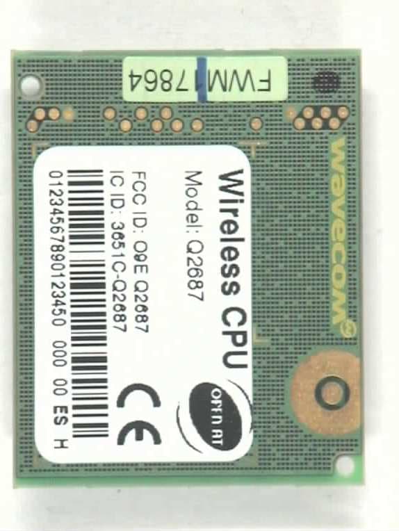
O9EQ2687
Nov 07, 2006Wireless CPU (850/900/1800/1900 MHz)
Equipment Class
PCB - PCS Licensed Transmitter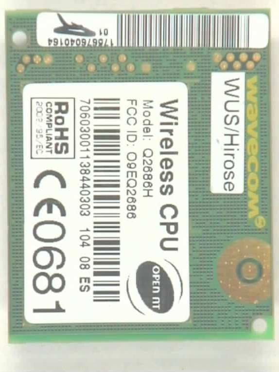
O9EQ2686
Apr 27, 2006Q2686
Equipment Class
PCB - PCS Licensed Transmitter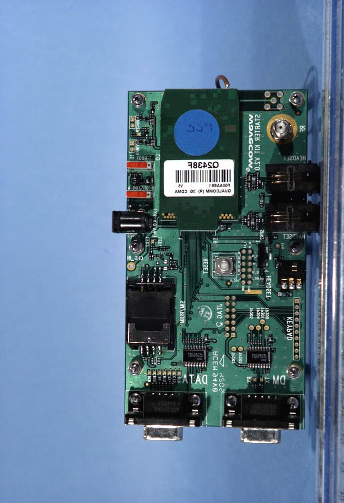
O9EQ2438F
May 13, 2004Tri-Mode Dual-Band CDMA Wireless Evaluation Kit
Equipment Class
PCB - PCS Licensed Transmitter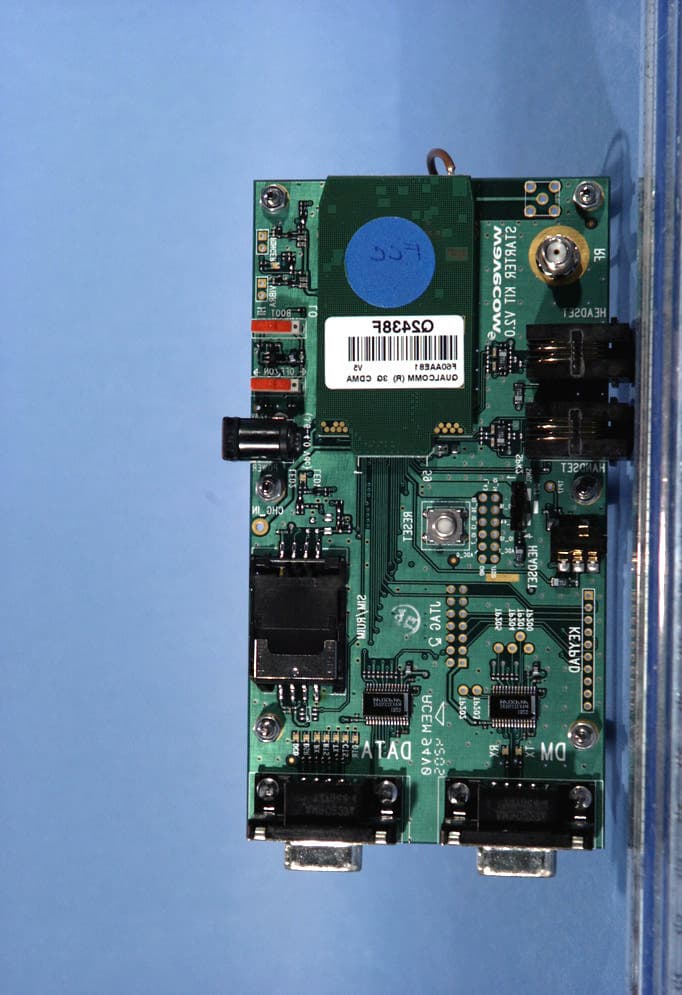
O9EQ2438
Nov 17, 2003Dual-Band CDMA Wireless Module Evaluation Kit
Equipment Class
PCB - PCS Licensed Transmitter