OB6-IGRS46D9916Data Reader
Hi-G-Tek Ltd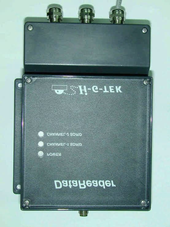
Click to zoom
Application Details
- Equipment Class
- LMS - Part 90 Location & Monitoring Transmitter
- Date of Grant
- Feb 23, 2004
- Application Purpose
- Original Equipment
- Date of Application
- Feb 23, 2004
- Equipment Note
- Data Reader
- Frequency Range
- 916.50000000 - 916.50000000
- Company
- Hi-G-Tek Ltd
- Country
- Israel
Documents & Files
Document Text
Text extracted from the exhibit documents filed with the FCC. Open a document above to read the original.
Users Manual
Hi-G-Tek Ltd. Microelectronics and Asset Tracking Technology User’s Manual Ver. A 61 UM4710 - 2 - Hi-G-Tek Ltd. Micro elec tro nic s & A sset Tra ck ing Te ch no logy 1 INTRO DUCTIO N....................................................................... 10 1.1 W HAT P RODUCTS ARE C OVERED BY TH IS M ANUAL .................. 10 1.2 A BOUT TH E P RO DU C T ............................................................... 10 1.3 S YSTEM C OMPONENTS .............................................................. 14 1.3.1 The Mounting Fixture............................................................ 14 1.3.2 The DataSeal ........................................................................ 14 1.3.3 Sealing Wire ......................................................................... 15 1.3.4 Outdoor DataReader.............................................................. 15 1.3.5 Indoor DataReader ................................................................ 17 2 Q UICK-START .......................................................................... 20 2.1 B EFORE YO U BEG IN ................................................................... 20 2.2 S ETT ING UP TH E D ATA R EADERS ............................................... 21 2.3 I NSTALLING TH E E VALUATION S OFTW ARE ............................... 21 2.4 C ONFIG URING TH E S YSTEM ...................................................... 22 2.5 P REPARING THE D ATA S EAL /D ATA T AG ..................................... 24 2.6 E X ECUTING A V ERIFY COMMAND .............................................. 27 2.7 A B RIEF T UTORIAL T HROUGH THE S TATES O F TH E D ATA S EAL 29 3 DATAS EAL INSTALLATIO N................................................... 34 4 DATATAG INSTALLATIO N..................................................... 38 4.1 P LACING THE D ATA T AG ON A V EH ICLE .................................... 38 4.1.1 Horizontal Orientation:.......................................................... 39 Hi-G-Tek Ltd. Micro electro nics & Asset Tracking Techno logy - 3 - 4.1.2 Vertical Orientation............................................................... 39 5 DATAREADER INSTALLATIO N ............................................. 42 5.1 O UTDOOR D ATA R EADER I NSTALLATIO N .................................. 42 5.1.1 Ceiling Inst allat ion................................................................ 42 5.1.2 Connecting the Outdoor Unit................................................. 43 5.1.3 Wiring the Outdoor DataReader ............................................. 44 5.1.4 RS-232 Wiring Diagram........................................................ 45 5.1.5 RS-485 Full Duplex Wiring Diagram...................................... 46 5.1.6 RS-485 Half Duplex Wiring Diagram..................................... 46 5.1.7 DataReader Configuration Switches ....................................... 46 5.2 I NDOOR D ATA R EADER I NSTALLATION ...................................... 47 5.2.1 Connecting the Indoor Unit.................................................... 47 5.2.2 Wiring the Indoor DataReader................................................ 48 5.2.3 RS-232 Wiring Diagram........................................................ 49 5.2.4 RS-485 Full Duplex Wiring Diagram...................................... 50 5.2.5 RS-485 Half Duplex Wiring Diagram..................................... 51 5.3 C HA IN ING D ATA R EADERS T O G E TH ER ...................................... 51 5.4 RS -2 32 /RS - 48 5 A DAPTER .......................................................... 54 5.4.1 Connecting the RS-232/RS-485 Adapter to the First DataReader 54 5.4.2 Connecting the RS-232/RS-485 Adapter to the Controlling Co mp ut er 5 6 5.5 P OWER S UPPLY R EQUIREMENTS ............................................... 56 5.5.1 General................................................................................. 56 5.5.2 Indoor Installation................................................................. 57 5.5.3 Outdoor Installation............................................................... 57 5.6 C ABLE S ELECTION .................................................................... 58 5.7 I NSTALLATIO N N O TES ............................................................... 59 5.8 D ATA R EADER O PERATION I NSTRUCTIONS ................................ 60 - 4 - Hi-G-Tek Ltd. Micro elec tro nic s & A sset Tra ck ing Te ch no logy 5.8.1 Power Indicators:.................................................................. 60 5.8.2 Channel 1 SD/RD Indicator:.................................................. 60 5.8.3 Channel 2 SD/RD Indicator:.................................................. 61 6 SYSTEM O VERVIEW................................................................ 64 6.1 S YSTEM DESCRIPTION ............................................................... 64 6.2 D ATA S EAL AND D ATA R EADER M ODES O F O PERATION ............. 66 6.2.1 DataSeal Modes of Operation................................................. 66 6.2.2 DataReader Modes of Operation............................................. 68 6.3 M OST C OMMON C OMMANDS AND S EA L S TATUS ....................... 69 6.3.1 Most Commonly Used Commands ......................................... 69 6.3.2 DataSeal's Status................................................................... 70 6.4 S YSTEM P LANNING ................................................................... 71 6.4.1 Electromagnetic Environment ................................................ 72 6.4.2 System Layout ...................................................................... 72 6.4.2.1 Radio Frequency Communication Layout. ............................ 73 6.4.2.2 Line Communication RS-485 Layout.................................... 74 6.5 S YSTEMS S EGREGATION ........................................................... 75 6.5.1 Companies Segregation by OrgID.......................................... 76 6.5.2 Departme…
Text truncated - open the document above for the full version.
Cover Letter(s)
FCC Confidentiality Form 9-Dec-03 To: Federal Communications Commission 7435 Oakland Mills Road Columbia, MD 21046 Gentlemen: This letter is to comply with Section 0.457(d)(2)(i) pertaining to confidential material. HI-G-TEK would like the following documents regarding this submission for FCC ID: OB6-IGRS46D9916 to be kept confidential. Main board schematic 47D10010 and RF board schematic 47D10100 The above material contains trade secrets or technical data, which would customarily be guarded from competitors. We do not want these documents to be accessible to the general public. Sincerely, __________________________________ Micha Auerbach President and CEO HI-G-TEK Ltd.
Cover Letter(s)
American Telecommunications Certification Body Inc. 6731 Whittier Ave, McLean, VA 22101 February 20, 2004 RE: FCC ID: OB6-IGRS46D9916_ATCB001131 Attention: Edward Usoskin I have a few comments on this Application. 1. Please note that the 731 states part 90 and part 15. The technical section of the manual states 15.249. Please be specific as to which rule part to which you wish this device certified. Please explain and please make documentation consistent. 2. Please note that you state the use of ANSI C63.4 as the test method. Please note that for part 90 this is not an appropriate test method (e.g. ANSI C63.4 is for unlicensed part 15 devices only). Please correct the test method and or test to the proper test method. 3. Please explain why conducted emissions to 15.207 were performed. 15.207 is the conducted emissions limits for intentional radiators under part 15. 4. Please note that the conducted emissions plots are far too wide and far to fast to provide adequate information on the compliance of this device. For example, the fundamental emission shows a reading of -67dBm (-37 if 30dB attenuation is applicable) when the actual emissions of the fundamental is far greater. This then leads to the question of compliance on other emissions shown on the plots. Conducted emissions at the antenna terminal needs to be done using a smaller span than provided. Please provide evidence that clearly shows compliance (use smaller spans and possibly longer sweep times to allow the analyzer to capture the actual signal and levels involved). Alternately, please explain and justify why a 700MHz span using a 230ms sweep is a valid and useable analyzer setting for taking appropriate conducted antenna terminal emissions measurements. Dennis Ward mailto:[email protected] The items indicated above must be submitted before processing can continue on the above referenced application. Failure to provide the requested information may result in application termination. Correspondence should be considered part of the permanent submission and may be viewed from the Internet after a Grant of Equipment Authorization is issued. Please do not respond to this correspondence using the email reply button. In order for your response to be processed expeditiously, you must submit your documents through the AmericanTCB.com website. Also, please note that partial responses increase processing time and should not be submitted. Any questions about the content of this correspondence should be directed to the sender.
Cover Letter(s)
HERMON LABORATORIES February 23, 2004 American TCB 6731 Whittier Ave Suite C110 McLean, VA 22101 Attn: Mr. D. Ward, Examining Engineer RE: your e-mail dated February 20, 2004; Hi-G-Tek Ltd. FCC ID:OB6-IGRS46D9916, ATCB001131 Dear Mr. Ward, Please find below the answers to your questions. 1) The corrected user manual User_Guide_15758_rev1 (please refer to page 240, §10.3) was uploaded on February 23, 2004 via User Manual folder. We apologize for this mistake. 2) The corrected test report without reference to ANSI, HIGRAD_FCC.15758_rev1 was uploaded on February 23, 2004. There is no restrictions neither for sweep time nor for sweep width in FCC rules relate to the tested equipment. All the measurements were performed in auto coupling mode as manufacturer (HP/Agilent) recommended and providing there is no other guidelines in FCC. The emission of transmitter was continuous, 40 kHz FSK modulated with 15625 bytes/second, and spectrum analyzer bandwidth was wider than 120 kHz, there was no way problem with auto coupled measurements might rise in this case. Regarding the test procedure for occupied bandwidth measurements, please advise which will be a relevant one as there is no reference to anyone at all in FCC part 90, neither to ANSI C63.4 nor to TIA/EIA-603-A. 3) Conducted emissions testing was performed as per FCC Part 15, 15.107. The corrected test report HIGRAD_FCC.15758_rev1 was uploaded on February 23, 2004. Sorry for printing mistake. 4) The emission meant in your comments (-67 dBm, Plot A7 of HIGRAD_FCC.15758 test report) is zoom of spurious (not carrier) emission provided in Plot A6 of the mentioned report. For output power please refer to Plot A1. Thank you for your patience and help. Sincerely, Marina Cherniavsky, certification engineer Hermon Laboratories
External Photos
FCC ID:OB6-IGRS46D9916 Date: February 2004 Page 1 of 3 EXTERNAL PHOTOGRAPHS This document contains 2 photographs FCC ID:OB6-IGRS46D9916 Date: February 2004 Page 2 of 3 Photograph No.1 Data reader front view FCC ID:OB6-IGRS46D9916 Date: February 2004 Page 3 of 3 Photograph No.2 Data reader rear side view
ID Label/Location Info
HGT5445 Made In Israel DataReader MODEL: IG-RS-46D9-916MODEL:IG-RS-46D9-916 FCC ID: OB6-IGRS46D9916FCCID:OB6-IGRS46D9916 0123456789 S/N POWER: 24V, 70mA 76.20 mm 38.10 mm Back side is permanent adhesiveBacksideispermanentadhesive This Device complies with Part 15 of the FCC Rules. Operation is subject to the following two conditions: (1) This device may not cause harmful interference, and (2) this device must accept any interference received, including interference that may cause undesired operation. ThisDevicecomplieswithPart15oftheFCCRules.Operationissubjecttothefollowingtwoconditions: (1) Thisdevicemaynotcauseharmfulinterference,and(2)thisdevicemustacceptanyinterference received, includinginterferencethatmaycauseundesiredoperation. HGT5468 Made In Israel DataReader MODEL: IG-RS-43D9-916MODEL:IG-RS-43D9-916 FCC ID: OB6-IGRS46D9916FCCID:OB6-IGRS46D9916 0123456789 S/N POWER: 24V, 70mA 76.20 mm 38.10 mm Back side is permanent adhesiveBacksideispermanentadhesive This Device complies with Part 15 of the FCC Rules. Operation is subject to the following two conditions: (1) This device may not cause harmful interference, and (2) this device must accept any interference received, including interference that may cause undesired operation. ThisDevicecomplieswithPart15oftheFCCRules.Operationissubjecttothefollowingtwoconditions: (1) Thisdevicemaynotcauseharmfulinterference,and(2)thisdevicemustacceptanyinterference received, includinginterferencethatmaycauseundesiredoperation. Label location FCC ID:OB6-IGRS46D9916
Internal Photos
FCC ID:OB6-IGRS46D9916 Date: February 2004 Page 1 of 10 INTERNAL PHOTOGRAPHS This document contains 9 photographs FCC ID:OB6-IGRS46D9916 Date: February 2004 Page 2 of 10 Photograph No.1 Data reader internal view FCC ID:OB6-IGRS46D9916 Date: February 2004 Page 3 of 10 Photograph No.2 Data reader internal view with LED PCB removed FCC ID:OB6-IGRS46D9916 Date: February 2004 Page 4 of 10 Photograph No.3 Data reader RF board Top view FCC ID:OB6-IGRS46D9916 Date: February 2004 Page 5 of 10 Photograph No.4 Data reader RF board Bottom view FCC ID:OB6-IGRS46D9916 Date: February 2004 Page 6 of 10 Photograph No.5 IG-RS-46D9-916 data reader main board Top view FCC ID:OB6-IGRS46D9916 Date: February 2004 Page 7 of 10 Photograph No.6 IG-RS-46D9-916 data reader main board Bottom view FCC ID:OB6-IGRS46D9916 Date: February 2004 Page 8 of 10 Photograph No.7 IG-RS-43D9-916 data reader main board Top view FCC ID:OB6-IGRS46D9916 Date: February 2004 Page 9 of 10 Photograph No.8 IG-RS-43D9-916 data reader main board Bottom view FCC ID:OB6-IGRS46D9916 Date: February 2004 Page 10 of 10 Photograph No.9 Data reader LED board Top view
Operational Description
Page 1 of 6 DataReader description 1. General 1.1. Reference documents: 1.1.1. Main board circuit diagram, document 47D10010 1.1.2. RF board circuit diagram , 47D10100 1.1.3. LEDs board circuit diagram 47D10090 1.2. Pages number referenced in the following description, are referred to the schematics. 2. Functional Description 2.1. The DataReader is used as an interrogator to the DataSeal. The DataReader communicates with the DataSeal by RF of 916.5MHz FSK modulated with 40KHz deviation. 2.2. The DataReader is powered by an external 24VDC power supply. 2.3. The DataReader has RS485 communication lines, so readers can be chained and be connected to a host. 2.4. An interrogation sequence can be initiated either by the host or by the DataReader independently. When an interrogation cycle starts, the DataReader transmits a header for 0.5-3Sec. Then it opens a receiving window for Trw seconds, typically 2sec. In this window, each DataSeal who received the DataReader message, replies with a short message, typically 10mS. 2.5. The DataReader contains 3 PCB’s. Digital motherboard, RF board and LEDs board. The motherboard includes all the digital control, power supply and serial communication circuitry. The RF board includes the RF transmitter, RF receiver and a ìP, which handle the base band processing. The LEDs boards include 3 LEDs for indications. Page 2 of 6 3. Mother Board Circuit description 3.1. Block Diagram 3.2. Page 3 of 6 3.3. ìP: (U1 Pg.2): 68HC812, main controller. 3.4. XTAL (Y1 Pg.2): 16MHz crystal, supply clock to the ìP. 3.5. RAM (U4A, U4B Pg.3): System RAM. 3.6. Flash (U5 Pg.3): System flash memory. 3.7. RTC (U3 Pg.3): Real time clock IC, it has an optional clock source, either a 32768Hz crystal (Y2) or 32768Hz oscillator (U6). This circuit is optional and not populated in the board. 3.8. Buzzer (BZ1 Pg.2): Piezo electric buzzer for audible alarm. This circuit is optional and not populated in the board. 3.9. Reset Control (U28 Pg.2): Reset control to the μP, includes power on reset and watch dog reset. 3.10. Reference Voltage (U2 Pg.2): reference voltage to A/D in the μP. 3.11. Back up circuitry (U7, BT1 Pg.3): This circuit supplies a back up voltage to RAM at power fail. This circuit is optional and not populated in the board. 3.12. Config Interface (U22, S1 Pg.4): a set of dip switches (S1) is used to determine DataReader operation mode. The switches are located in the bottom portion of the DataReader, so the user can determine the mode of operation. (See user manual parag. 3.1). The signals from the dip switches are protected by transient suppressor (U29) and by RC network (C39-C44, R98-R103, R119-R124). 3.13. I/O interface (U23, TB3, Pg.4): Terminal block TB3 is used to connect the I/O to the DataReader. The μP writes the outputs by latch (U23). There are 3 kinds of outputs: 3.13.1. 1 direct drive to a LED (Q4, TB3-10). 3.13.2. 2 optically isolated outputs (U25, U26, TB3-18, 22). 3.13.3. 1 Dry contact output ( K1,TB3- 26-30) There are 2 kinds of inputs: 3.13.4. 1 optically isolated input ( U24,TB3-14) 3.13.5. 1 non isolated, used as external interrupt. 3.14. RS485 Interface (Pg. 5): Isolated RS485 circuitry is used. Signals are optically isolated by U12-U15; power is supplied by U11 and isolated by T1. Signals are buffered by U16, U17. S3 is configurable by user and determines half or full duplex application. S2 is configurable by user and connects termination resistor R71 when required in a RS485 chain. Page 4 of 6 3.15. RS232 interface (U9, Pg.5): RS232 interface (U9) is optional on the board; also power kick start circuit (Q5) is used in applications where power off stand by mode is required. This circuit is optional and not populated in the board. 3.16. Piggy Back Board Interface (Pg. 6) Mother board can accept two piggyback boards; a pair of connectors are assigned to each board (JA1-2, JB1-2). All circuitry in Pg. 2 includes data lines and control lines between boards. 3.17. Isolated Power Supply (U19, Pg.7): Switching power supply module (U19) is used as 5V supply to all circuitry. F1, F2 are non serviceable 1A fuses, D10 provides reverse polarity protection, D11 provides transients protection and Q7 functions soft start to limit inrush current during start up. S4 is DIP switch, which can be used by the user to shut down individual DataReader in chain for service. 3.18. Non Isolated Power Supply (U18, Pg.7): A non isolated power supply (U18), is optional on board. This circuit is optional and not populated in the board. Page 5 of 6 4. RF Board Circuit Description 4.1. Block Diagram Page 6 of 6 4.2. ìP (U1 Pg.2): RF board μP with 4MHz crystal. 4.3. Temperature sensor (U6, Pg.2): The IC supply analog voltage, which represents temperature, to the ìP. 4.4. Voltage regulators: The RF board supply comes from the man board. The RF board includes linear regulators to different parts of the board. U8, U19 Pg.2 supply voltage to the RF circuitry. U23 Pg.3 is optional, and not populated. U24 Pg.4 is optional and not populated. 4.5. Antenna switch (U10 Pg.3): The antenna switch is controlled by the ìP; it switches the antenna between transmitter and receiver. 4.6. Receiver (Pg.3): The received RF signal goes through the antenna switch (U10) then to a band pass filter (U16), amplifier (U12) and receiver IC U13. The receiver includes a local oscillator of 26.641176MHz (U27). The data channel through the receiver IC includes 10.7MHz IF which is filtered by Y4, and a discriminator circuit Y5, D6. The output of the receiver IC, is digitized with U28 and U29, then goes to the ìP. ( Crystal Y3 is optional, and not populated ) 4.7. Transmitter (Pg. 4): A 26.64062MHz crystal (Y6) is connected to the transmitter IC (U15). The transmitter generates a 916.5MHz carrier, FSK modulated, with ±20KH deviation. Data is supplied by the ìP. The RF signal goes to a voltage controlled power amplifier, to a transformer (U20) and through the antenna switch (U10 Pg.3) to the antenna. The RF power is sample…
Text truncated - open the document above for the full version.
Operational Description
I=35mA V=3.6V Power AmplifierPowerAmplifier Voltages and currents Page 4/4 of schematic Voltagesandcurrents Page 4/4ofschematic
Parts List/Tune Up Info
LevelP/NREFQtyRevDescription 0SA4602D931 A00OD RF916FCC90 PCB ASSY -1C0R5N616C15,16,47,55,6150 CAP 0.5PF NPO 0603 -1C100N6C90,9120 CAP10PF NPO 50V 0603 -1C101N650C12,46,49,97,54110 CAP100PF NPO50V 0603 ,58,73,74,89, CU12B,R61 -1C102N650C9,19,20,3140 CAP 1NF 50V NPO 0603 -1C102X616C24,30,32,36,42140 CAP 1nF 16V X7R 0603 44,52,65,CU12A, CU13A-E -1C103X6C5,50,5730 CAP 10NF 50V X7R0603 -1C104X616C6,7,72,CU1A-C,170 CAP 0.1MF 16VX7R0603 CU2A-B,CU3-7,9, 25, 27,28 -1C105TA25C8,7720 CAP1MF/25V TANT.CS-A -1C105X010C43,5120 CAP 1MF 10V X7R 0805 -1C107TE16C1010 CAP.100MF 16V20% C-E -1C120N616C6210 CAP 12PF16V NPO 0603 -1C152X650C87,9420 CAP 1.5NF 0603X7R50V -1C180N616C29,6420 CAP18PF 16V NPO 0603 -1C1R2N616C9510 CAP1.2PF NPO16V 0603 -1C1R5N616C17,26,27,3740 CAP1.5PF NPO16V 0603 -1C1R8N616C2510 CAP 1.8PF16VNPO 0603 -1C200N616C6010 CAP 20PF16V NPO 0603 -1C220N616C1,320 CAP 22PF NPO16V 0603 -1C2R7N616C4810 CAP2.7pF NPO16V 0603 -1C331N650CU15A,CU15B20 CAP330PF50V NPO 0603 -1C333X616C3510 C 33nF 16V X7R 0603 -1C336T825C6610 CAP TAN.33MF/25V RAD -1C390N616C7910 CAP39PF 16V NPO 0603 -1C470N650C9210 CAP 47PF 50V 0603 -1C471N650C10010 CAP470PF50V NPO 0603 -1C681N616C3810 C 680pF 16V NPO 0603 -1D2822D410 HMPS-2822 MINIPACK -1DX914AU2110 DIODE 1N914 SOT23 -1DZMV932D610 ZMV932TA SOD-323 -1E47007011303 EMBD.SFTWR D.RDR RU1 -1F107MA5Y410 FILTER 10.7MHz 280KH -1FR25061L11,1520 SMT BEAD300 OHM 0603 -1HGT3049CV210 TRIMMER CAP 2-6PF -1HGT5162J110 MM106 STRAIGHT FEMAL -1HGT56270.0010 MS-472N CONFRML.COAT -1J37413JP210 HDR 1X3 STRIT 100CTR -1L0100EL910 CHIP IND. 10nH 0603 -1L0120EL12,1420 CHIP COIL 12nH 0603 -1L0150EL2,420 CHIP IND. 15nH 0603 -1L1000EL6,720 CHIP IND 100nH 0603 -1L4R70EL510 CHIP COIL 4.7nH 0603 -1L6R80EL10,1320 CHIP COIL 6.8nH 0603 -1L8R70EL110 CHIP COIL 8.7nH 0603 Page 1 of 2 -1NFHD2X7JP110 FEMALE HEADER 2X7 -1NHD2X3JP310 HEADER 2X3 0.1" -1NHD2X7PA1,PA220 HEADER 2X7 0.1" -1P470071 CPCB4LAY.128X50X1.6mm -1Q3906AQ2,320 TRN.2N3906 SOT-23 -1R000JLR65-67,85,88,60 RES 0 OHM 0603 C88 -1R1003AR15,16,24,26,2870 RES 100K 1% 0805 63,64 -1R101JLR36,44,7130 RES 100 OHM 5% 0603 -1R102JLR35,48,8430 SMT RES 1K 5% 0603 -1R103JLR6,7,10,13,38,60 SMT RES 10K 5% 0603 74 -1R104JLR8,9,32,33, 76,70 SMT RES 100K 5% 0603 82,83 -1R2003AR5110 RES 200K 1% 0805 -1R202JLR37,4620 RES 2K 5% 0603 -1R2200BR10010 RES 220 OHM 5% 1206 -1R221JLR1110 RES 220 5% 0603 -1R272JLR8910 RES 2.7K 5% 0603 -1R303JLR7510 RES 30K OHM 5% 0603 -1R331JLR4,5,12,1440 RES 330 OHM 5% 0603 -1R472JLR60,6820 RES 4.7K 5% 0603 -1R510JLR8010 RES 51 OHM 5% 0603 -1R514JLR31,3420 RES 510K OHM 5% 0603 -1R684JLR77,7820 RES 680K 5% 0603 -1TSMT6-1U2010 SM-T6 COUPLER -1U2272ACDU4,7,2530 IC TLC2272ACD SO8 -1U24C02U910 IC S-24C02AFJ SO-8 -1U2980S36U8,1920 LP2980IM5-3.6SOT23-5 -1U4504DU210 IC MC14504BD SO16 -1U6004SU310 MAX6004EUR SOT-23 -1U9075EUKU2810 MAX9075EUK-T SOT23-5 -1ULS85354AIU110 AT90LS85354AI 44TQFP -1URF2302U1410 RF2302 MSOP-8 -1URF2436U1010 RF2436 SOT23-5 -1URF2442U1210 RF2442 RF-AMP NSOP8 -1UTH7108U1510 IC TRN.TH7108 SSOP16 -1UTH71112U1310 TH71112 LQFP-32 -1UTMP36FSU610 UTMP36FS SO8 -1UX9C104SIU510 X9C104SI SO8 -1Y107MG18Y510 CDACV10M7GA046-RO -1Y26641176PU2710 TCXO26.641176MHzDL14 -1Y2864062BY610 XTL 28.64062MHz 11PF -1Y4000AIY110 XTAL 4MHz IND.HC49/U -1YF1181U1610 FILTER916.5MHZ TO39 Page 2 of 2
Parts List/Tune Up Info
Document No Title Name & sign Date HGT200-464 Drawn SA4602D93 Max power test Procedure Rev Checked A Page 1 Approved Of 2 Project Date 11-Feb-04 1. General 1.1. The test procedure is applicable for RF board p/n SA4602D93 2. Equipment 2.1. Desktop power supply 24VDC/2A. 2.2. HP-E4411B Spectrum Analyzer. 2.3. Accessories Test Kit p/n QA063 including: 2.3.1. RS232 Digital Board. 2.3.2. 2x RF Cable p/n QA063/C 2.3.3. Serial comm. cable. 2.3.4. 10db attenuator. 2.4. PC with STARCORE test software 3. Test Fixture: 3.1. Connect the Power supply positive to TB1(1), and the negative to TB1(2). 3.2. Connect the serial comm. cable to PC. 3.3. Connect the RF board under test to the socket on the digital PCB. 3.4. Connect the RF cable and the 10db attenuator between the RF board antenna connector and the spectrum analyzer input. 3.5. On the spectrum analyzer load the setup program 916MAXPWR.STA (Parameters included: Center frequency 916.5MHz, Resolution bandwidth: 300KHz, Amplitude compensation for cable & Attenuator) Ref digital board RF Board Under test Spectrum Analyzer PC 10db Attenuator RS232 Power Supply Page : 2 Rev Date Document No. of : 2 A 11-Feb-04 HGT200-464 4. Test Procedure 4.1. Turn ON the power supply, run the test software. Wait until power up sequence ended. 4.2. Program RF power to 255 (maximum value). 4.3. Connect jumper at JP3(5-6). 4.4. Press MAX-HOLD, wait 3-4 Seconds and press PEAK-SEARCH. 4.5. Verify reading 19.5mW. If power is more then 19.5mW change R76 to 110K and repeat the test. If still fails, change R76 to 120K and repeat the test. If still fails, board is rejected. 4.6. Disconnect the jumper at JP3(5-6). 4.7. Program RF power to 125 (default Transmission power). 4.8. Power off the power supply.
Test Report
This report is in conformity with ISO/IEC 17025. The A2LA logo endorsement applies only to the test methods and the standards that are listed in the scope of Hermon Laboratories accreditation. The test results relate only to the items tested. This test report must not be reproduced in any form except in full with the approval of Hermon Laboratories Ltd. Page 1 of 81 Document ID: HIGRAD_FCC.15758_rev1.doc Date of Issue: February 2004 HERMON LABORATORIES Electrical Hermon Laboratories Ltd. P.O.Box 23 Binyamina 30500, Israel Tel.+972 4628 8001 Fax.+972 4628 8277 e-mail: [email protected] ELECTROMAGNETIC EMISSIONS TEST REPORT according to 47CFR Part 90, subpart I and part 15, subpart B for Hi-G-TEK Ltd. EQUIPMENT UNDER TEST: Data reader Models:IG-RS-46D9-916, IG-RS-43D9-916 Page 2 of 81 Document ID: HIGRAD_FCC.15758_rev1.doc Date of Issue: February 2004 HERMON LABORATORIES Hermon Laboratories Ltd. P.O.Box 23 Binyamina 30500, Israel Tel.+972 4628 8001 Fax.+972 4628 8277 e-mail: [email protected] Contents 11 Project informationProject information..........................................................................................................................................................................................................33 22 Summary and signaturesSummary and signatures..........................................................................................................................................................................................44 33 EUT descriptionEUT description..................................................................................................................................................................................................................55 3.1 GENERAL DESCRIPTION........................................................................................................................................................5 3.2 EUT TEST CONFIGURATION..................................................................................................................................................5 44 Test resultsTest results..............................................................................................................................................................................................................................88 4.1 PEAK OUTPUT POWER TEST ACCORDING TO PART 90 §90.205(K)..........................................................................................8 4.2 OCCUPIED BANDWIDTH ACCORDING TO PART 90 §90.209(5)................................................................................................9 4.3 EMISSION MASK AND RADIATED SPURIOUS EMISSIONS TEST ACCORDING TO PART 90 §90.210(K)(3)....................................10 4.4 UNINTENTIONAL RADIATED EMISSIONS TEST ACCORDING TO §15.109..................................................................................13 4.5 FREQUENCY STABILITY MEASUREMENT ACCORDING TO §90.213.........................................................................................15 4.6 CONDUCTED EMISSIONS TEST ACCORDING TO §15.207, 15.107.........................................................................................17 Appendix A PlotsAppendix A Plots........................................................................................................................................................................................................................2121 Appendix B Test equipment used for testsAppendix B Test equipment used for tests......................................................................................................................................................6363 Appendix C Antenna factors and cable lossAppendix C Antenna factors and cable loss....................................................................................................................................................6565 Appendix D General informationAppendix D General information..................................................................................................................................................................................8181 TEST FACILITY DESCRIPTION.........................................................................................................................................................81 ABBREVIATIONS AND ACRONYMS...................................................................................................................................................81 SPECIFICATION REFERENCES........................................................................................................................................................81 Page 3 of 81 Document ID: HIGRAD_FCC.15758_rev1.doc Date of Issue: February 2004 HERMON LABORATORIES Hermon Laboratories Ltd. P.O.Box 23 Binyamina 30500, Israel Tel.+972 4628 …
Text truncated - open the document above for the full version.
Contact Information
Applicant
Roni Cohen(Hardware Department Manager)
Technical Contact
Hermon LaboratoriesEdward Usoskin
[email protected]972 4628 8001
Harakevet Industrial zone · Binyamina · Israel
Technical Specifications
| # | Rule Parts | Frequency Range | Power Output | Emission | Tolerance |
|---|---|---|---|---|---|
| 1 | 90.353 | 916.5 MHz - 916.5 MHz | 20.00 mW | 138KFID | 2.5000000000 ppm |
Other Applications from Hi-G-Tek Ltd

OB6-IGSV40916
Dec 25, 2013SPDS SEAL
Equipment Class
DXX - Part 15 Low Power Communication Device Transmitter
OB6-IGST51433
Jan 18, 2010ISO 18000-7 SENSOR TRANSPONDER
Equipment Class
DSC - Part 15 Security/Remote Control Transmitter
OB6-IGST50433
Jan 18, 2010ISO 18000-7 SECURITY TRANSPONDER
Equipment Class
DSC - Part 15 Security/Remote Control Transmitter
OB6-IGRF97433
Jan 03, 2010ISO-18000- FIXED RFID INTERROGATOR
Equipment Class
DSR - Part 15 Remote Control/Security Device Transceiver
OB6-IGMA125IS
Feb 26, 2008IS Micro Reader
Equipment Class
DCD - Part 15 Low Power Transmitter Below 1705 kHz