OEOTLSR825XML32DModule
Telink Semiconductor (Shanghai) Co., Ltd.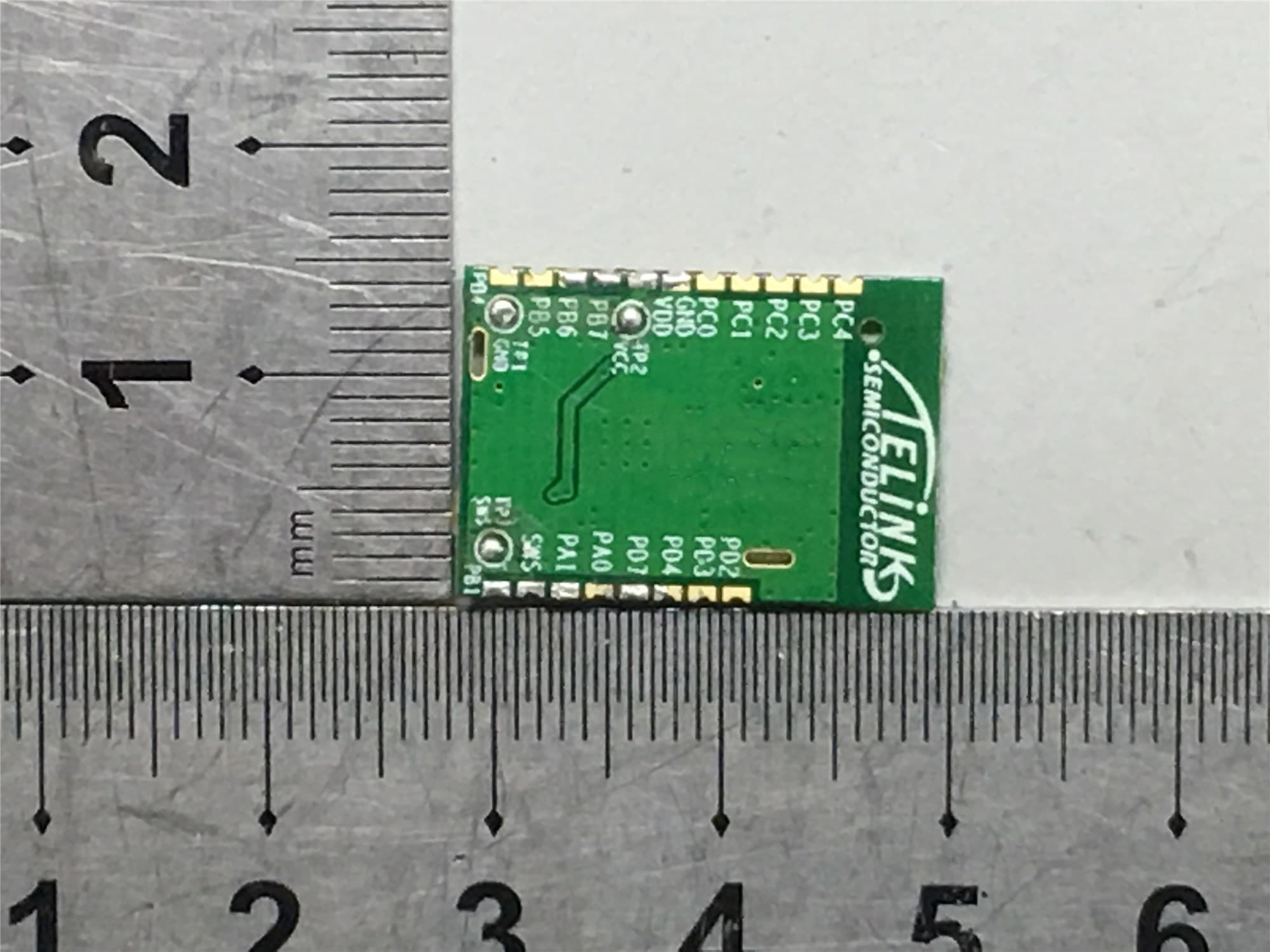
Click to zoom
Application Details
- Equipment Class
- DTS - Digital Transmission System
- Date of Grant
- Feb 03, 2020
- Application Purpose
- Original Equipment
- Date of Application
- Feb 03, 2020
- Equipment Note
- Module
- Frequency Range
- 2402.00000000 - 2480.00000000
- Country
- China
Documents & Files
Document Text
Text extracted from the exhibit documents filed with the FCC. Open a document above to read the original.
Users Manual
Telink Module TLSR825XML32D User Manual 2019/4/9 TELINK SEMICONDUCTOR Keyword: Features; Pin connection; User manual Brief: This is a user manual for Telink 825X Module TLSR825XDB48. Telink Module TLSR825XML32D User Manual 1 Published by Telink Semiconductor Bldg 3, 1500 Zuchongzhi Rd, Zhangjiang Hi-Tech Park, Shanghai, China © Telink Semiconductor All Right Reserved Legal Disclaimer This document is provided as-is. Telink Semiconductor reserves the right to make improvements without further notice to this document or any products herein. This document may contain technical inaccuracies or typographical errors. Telink Semiconductor disclaims any and all liability for any errors, inaccuracies or incompleteness contained herein. Copyright (c) 2019 Telink Semiconductor (Shanghai) Ltd, Co. Information: For further information on the technology, product and business term, please contact Telink Semiconductor Company (www.telink-semi.com). For sales or technical support, please send email to the address of: [email protected] [email protected] Telink Module TLSR825XML32D User Manual 2 Table of contents 1 Product Introduction .............................................................................................. 3 1.1 General description .......................................................................................... 3 1.2 Key features ..................................................................................................... 3 2 Pin Connection Guide ............................................................................................. 8 2.1 Supply power ................................................................................................... 8 2.2 Download firmware ......................................................................................... 9 2.3 Test RF signal .................................................................................................... 10 1.3 GPIO Pin layout ................................................................................................ 5 Telink Module TLSR825XML32D User Manual 3 1 Product Introduction This is a user manual for Telink Module TLSR825XML32D. 1.1 General description The TLSR825XML32D, which is based on Telink TLSR825XF512ET32 chip, provides a BLE wireless system. The TLSR825XML32D integrates a power-balanced 32-bit MCU, BLE, 64kB SRAM, 512kB internal Flash, 14bit ADC with PGA, analog and digital microphone input, stereo audio output, 6-channel PWM, one quadrature decoder (QDEC), abundant and flexible GPIO interfaces, and nearly all the peripherals needed for IoT (Internet of Things) and HID (Human Interface Devices) application development (e.g. Bluetooth Low Energy). The TLSR825XML32D supports standards and industrial alliance specifications including Bluetooth Low Energy (up to Bluetooth 5). Telink TLSR825XML32D board can be used for SDK development. Firmware can be directly downloaded to the TLSR825XML32D board to be up and running. 1.2 Key features Bluetooth 5 Compliant, 1Mbps, 2Mbps, Long Range 125kbps and 500kbps 64kB on -chip SRAM with up to up to 32kB retention 512kB internal Flash A rich set of I/Os: SPI, I2C , S ingle wire, up to 17 GPIOs, UART with hardware flow control and 7816 protocol support, DMIC (Digital Mic), AMIC (Analog Mic), I2S, Telink Module TLSR825XML32D User Manual 4 Stereo Audio output 6-channel PWM (Pulse Width Modulation) output 6-channel (only GPIO input), 14-bit SAR ADC with 10.5-bit ENOB 4-channel PGA, differential input Tx output power: Typ. +9.47dBm RSSI monitoring with +/-1dB resolution Power supply: DC3.3V Telink TLSR825XML32D User Manual 5 1.3 GPIO Pin layout Figure 1 Pin layout Pin definition is shown as the Table 1: Table 1 Pin definition Pin No Module Pin Name Chip Pin Name Description J1 1 TL_GPIO2 SPI_CN/I2S_LR/PWM3/PD<2> SPI chip select (Active low) / I2S left right channel select / PWM3 output / GPIO PD[2] 2 TL_GPIO1 PWM1_N/I2S_SDI/7816_TRX (UART_TX)/PD<3> PWM1 inverting output / I2S serial data input / UART 7816 TRX (UART_TX) / GPIO PD[3] 3 TL_GPIO0 SWM/I2S_SDO/PWM2_N/ PD<4> Single wire master / I2S serial data output / PWM2 inverting output / GPIO PD[4] 4 TL_Grant SPI_CK/I2S_BCK/7816_TRX (UART_TX)/PD<7> SPI clock (I2C_SCK) / I2S bit clock / UART 7816 TRX (UART_TX) / GPIO PD[7] 5 TL_Priority DMIC_DI/PWM0_N/UART_RX/ PA<0> DMIC data input / PWM0 inverting output / UART_RX / GPIO PA[0] 6 TL_Request DMIC_CLK/7816_CLK/I2S_CLK/ PA<1> DMIC clock / UART 7816 clock / I2S clock / GPIO PA[1] Telink TLSR825XML32D User Manual 6 Pin No Module Pin Name Chip Pin Name Description 7 TL_SWS SWS/UART_RTS/PA<7> Single wire slave/ UART_RTS / GPIO PA[7] 8 TL_UTX PWM4/UART_TX/ATSEL2/lc_comp _ain<1>/sar_aio<1>/PB<1> PWM4 output / UART_TX / Antenna select pin 2 / Low power comparator input / SAR ADC input / GPIO PB[1] J2 1 TL_C4 PWM2/UART_CTS/PWM0_N/ sar_aio<8>/BIAS/PC<4> PWM2 output / UART_CTS / PWM0 inverting output / SAR ADC input / AMIC BIAS / GPIO PC[4] 2 TL_C3 PWM1/UART_RX/I2C_SCK/XC32K_ I/PGA_N1/PC<3> PWM1 output / UART_RX / I2C serial clock / (optional) 32kHz crystal input / PGA right channel negative input / GPIO PC[3] 3 TL_C2 PWM0/7816_TRX(UART_TX)/I2C_ SDA/XC32K_O/PGA_P1/PC<2> *1 PWM0 output / UART 7816 TRX (UART_TX) / I2C serial data / (optional) 32kHz crystal output / PGA right channel positive input / GPIO PC[2] 4 TL_C1 I2C_SCK/PWM1_N/PWM0/ PGA_N0/PC<1> I2C serial clock / PWM1 inverting output / PWM0 output / PGA left channel negative input / GPIO PC[1] 5 TL_C0 I2C_SDA/PWM4_N/UART_RTS/ PGA_P0/PC<0> I2C serial data / PWM4 inverting output / UART_RTS / PGA left channel positive input / GPIO PC[0] 6 GND Ground 7 TL_VDD VDD_IO/VDD3/VDDIO_AMS 3.3V power supply 8 TL_URX SDM_N1/SPI_DO/UART_RX/ lc_comp_ain<7>/sar_aio<7>/ PB<7> SDM negative output 1 / SPI data output / UART_RX / Low power comparator input / SAR ADC input / GPIO PB[7] 9 TL_B6 SDM_P1/SPI_DI/UART_RTS/ lc_comp_ain<6>/sar_aio<6>/ PB<6> SDM positive output 1 / SPI d…
Text truncated - open the document above for the full version.
Attestation Statements
Company: Telink Semiconductor (Shanghai) Co., Ltd. Add: Bldg 3, No. 1500, Zuchongzhi Rd, Zhangjiang Hi-tech Park, Shanghai 201203, China Tel: +862120281118 Fax: +862150388081 DECLARATION Dear Sir or Madam: The R F ch ip, mo del: TLSR825X, installed in our product module ,(model name: TLSR825XML32D. FCC ID: OEOTLSR825XML32D). The chip support BLE, Zigbee, 2.4G proprietary functions, But our product is only actived BLE function. Zig bee an d 2.4G proprietary functions have be shielded by software. Please contact me if there is need for any additional clarification or information. Best Regards, Signature: Print Name: Li Xiang Title: Manager FEDERAL COMMUNICATIONS COMMISSIONS Authorization and Evaluation Division 74 35 Oakland Mi lls Road Columbia, MD 21046
Cover Letter(s)
QA-FR-170-B Company: Telink Semiconductor (Shanghai) Co., Ltd. Add: Bldg 3, No. 1500, Zuchongzhi Rd, Zhangjiang Hi-tech Park, Shanghai 201203, China Tel: +862120281118 Fax: +862150388081 FCC Authorization Date: 2019-12-13 FE DERAL COMMUNICATIONS COMMISSION Authorization and Evaluation Division 7435 Oakland Mills Road Columbia, MD 21046 Subject: Agent Authorization To whom it may concern: We, Telink Semiconductor (Shanghai) Co., Ltd., the undersigned, Hereby authorizes Bay Area Compliance Laboratories Corporation to act on its behalf in all matters relating to application for Equipment authorization, including the signing of all documents relating to these matters. All acts carried out by Bay Area Compliance Laboratories Corp. on our behalf shall have the same effect as our own action. We, the undersigned, hereby certify that we are not subject to a denial of federal benefits, that includes FCC benefits, pursuant to Section 5301 of the Anti-Drug Abuse Act of 1988, 21 U.S.C. 862. This authorization is valid until further written notice from the applicant. Sincerely Yours, Signature: Typed or Printed Name: Xiang Li Title: Manager
Cover Letter(s)
Company: Telink Semiconductor (Shanghai) Co., Ltd. Add: Bldg 3, No. 1500, Zuchongzhi Rd, Zhangjiang Hi-tech Park, Shanghai 201203, China Tel: +862120281118 Fax: +862150388081 E-mail: xiang.li@telin k-semi.com FCC Confidential Authorization Date: 2019-12-13 FEDERAL COMMUNICATIONS COMMISSIONS Authorization and Evaluation Division 7435 Oakland Mills Road Columbia, MD 21046 Subject: Confidentiality Request regarding application for certification of FCC ID: OEOTLSR825XML32D To: whom it may concern, In accordance with Sections 0.457 and 0 .459 of the Commission’s Rules, Telink Semiconductor (Shanghai) Co., Ltd. hereby requests long-term confidential treatment of information accompanying this application as outlined below: Block Diagram Schematics Operation Description The above materials contain proprietary and confidential information not customarily released to the public. The public disclosure of these materials provides unjustified benefits to its competitors in the market. Sincerely Yours, Signature: Typed or Printed Name: Xiang Li Title: Manager
Cover Letter(s)
Applicant Telink Semiconductor (Shanghai) Co., Ltd. FCC ID: OEOTLSR825XML32D Section 15.212 Modular Transmitters Request for Modular Approval Request for Limited Modular Approval RequirementsEUT ConditionsComply(Y/N) Single Modular Approval Requirements 1 The radio elements of the modular transmitter must have their own shielding. The physical crystal and tuning capacitors may be located external to the shielded radio elements. Refer to external photos. This module has shield cover. Y 2 The modular transmitter must have buffered modulation/data inputs (if such inputs are provided) to ensure that the module will comply with part 15 requirements under conditions of excessive data rates or over‐modulation. All inputs to the modules are buffered through logic or microprocessor inputs. Refer to Schematics. Y 3 The modular transmitter must have its own power supply regulation. The Module uses the chip TLSR825X with built-in power management components, the module rated power is 3.3V power, Refer to schematics. Y 4 The modular transmitter must comply with the antenna and transmission system requirements of §§15.203, 15.204(b) and 15.204(c). The antenna must either be permanently attached or employ a “unique” antenna coupler (at all connections between the module and the antenna, including the cable). The “professional installation” provision of §15.203 is not applicable to modules but can apply to limited modular approvals under paragraph (b) of this section. The modular transmitter has a PCB antenna arrangement for BLE, Refer to internal photo. Y Company: Telink Semiconductor (Shanghai) Co., Ltd. Add: Bldg 3, No. 1500, Zuchongzhi Rd, Zhangjiang Hi-tech Park, Shanghai 201203, China Tel: +862120281118 Fax: +862150388081 E-mail: [email protected] 5 The modular transmitter must be tested in a stand‐alone configuration, i.e., the module must not be inside another device during testing for compliance with part 15 requirements. Unless the transmitter module will be battery powered, it must comply with the AC line conducted requirements found in §15.207. AC or DC power lines and data input/output lines connected to the module must not contain ferrites, unless they will be marketed with the module (see §15.27(a)). The length of these lines shall be the length typical of actual use or, if that length is unknown, at least 10 centimeters to insure that there is no coupling between the case of the module and supporting equipment. Any accessories, peripherals, or support equipment connected to the module during testi ng shall be unmodified and commercially available (see §15.31(i)). The modular transmitter is connected to the controlled board when testing. Please refer to setup photo. Y 6 If using a permanently affixed label, the modular transmitter must be labeled with its own FCC identification number, and, if the FCC identification number is not visible when the module is installed inside another device, then the outside of the device into which the module is installed must also display a label referring to the enclosed module. This exterior label can use wording such as the following:“ContainsTransmitter Module FCC ID: OEOTLSR825XML32D”Any similarwording that expresses the same meaning may be used. The Grantee may either provide such a label, a n exa mple of which must be included Refer to the label. Y in the application for equipment authorization, or, must provide adequate instructions along with the module which explain this requirement. In the latter case, a copy of these instructions must be included in the application for equipment authorization. 7 The modular transmitter must comply with any specific rules or operating requirements that ordinarily apply to a complete transmitter and the manufacturer must provide adequate instructions along with the module to explain any such requirements. A copy of these instructions must be included in the application for equipment authorization. Refer to manual Y 8 Y Sincerely, Signature: Typed or Printed Name: Xiang Li Title: Manager The modular transmitter must comply with any applicable RF exposure requirements in its final configuration. The EUT meets RF exposure evaluation § 2.1091, If the device built into a host as a portable usage, the additional RF exposure evaluation may be required as specified by§ 2.1093
External Photos
EXHIBIT A - EUT EXTERNAL PHOTOGRAPHS Antenna
Internal Photos
EXHIBIT B - EUT INTERNAL PHOTOGRAPHS
RF Exposure Info
Bay Area Compliance Laboratories Corp. (Kunshan) Report No.: RSHA191213004-00A FCC Part 15.247 Page 12 of 52 FCC §1.1310& §2.1091 - MAXIMUM PERMISSIBLE EXPOSURE (MPE) Applicable Standard According to subpart 15.247(i) and subpart §1.1310, systems operating under the provisions of this section shall be operated in a manner that ensures that the public is not exposed to radio frequency energy level in excess of the Commission’s guidelines. Limits for Maximum Permissible Exposure (MPE) (§1.1310, §2.1091) (B) Limits for General Population/Uncontrolled Exposure Frequency Range (MHz) Electric Field Strength (V/m) Magnetic Field Strength (A/m) Power Density (mW/cm 2 ) Averaging Time (minutes) 0.3-1.34 614 1.63 *(100) 30 1.34-30 824/f 2.19/f *(180/f²) 30 30-300 27.5 0.073 0.2 30 300-1500 / f/1500 30 1500-100,000 / 1.0 30 f = frequency in MHz; * = Plane-wave equivalent power density; According to §1.1310 and §2.1091 RF exposure is calculated. Calculated Formulary: Predication of MPE limit at a given distance S = PG/4πR² = power density (in appropriate units, e.g. mW/cm 2 ); P = power input to the antenna (in appropriate units, e.g., mW); G = power gain of the antenna in the direction of interest relative to an isotropic radiator, the power gain factor, is normally numeric gain; R = distance to the center of radiation of the antenna (appropriate units, e.g., cm); Calculated Data: Frequency Range (MHz) Antenna Gain Tune-up Conducted Power Evaluation Distance (cm) Power Density (mW/cm 2 ) MPE Limit (mW/cm 2 ) (dBi) (numeric) (dBm) (mW) 2402~2480 0.00 1.00 9.50 8.91 20 0.0018 1.0 Note: For the above tune up power were declared by the manufacturer. Conclusion: The EUT meets exemption requirement- RF exposure evaluation greater than 20cm distance specified in § 2.1091. If the device built into a host as a portable usage, the additional RF exposure evaluation may be required as specified by§ 2.1093.
Test Report
Note: This test report is prepared for the customer shown above and for the device described herein. It may not be duplicated or used in part without prior written consent from Bay Area Compliance Laboratories Corp. This report is valid only with a valid digital signature. The digital signature may be available only under the Adobe software above version 7.0. FCC PART 15.247 TEST REPORT For Telink Semiconductor (Shanghai) Co., Ltd. Bldg 3, No. 1500, Zuchongzhi Rd, Zhangjiang Hi-tech Park, Shanghai 201203, China FCC ID: OEOTLSR825XML32D Report Type: Original Report Product Type: module Test Engineer: Nolan Xu Report Number: RSHA191213004-00A Report Date: 2020-01-03 Reviewed B y: Oscar Ye EMC Manager Prepared By: Ba y Area Compliance Laboratories Corp. (Kunshan) No.248 Chenghu Road,Kunshan,Jiangsu province,China Tel: +86-0512-86175000 Fax: +86-0512-88934268 www.baclcorp.com.cn Bay Area Compliance Laboratories Corp. (Kunshan) Report No.: RSHA191213004-00A FCC Part 15.247 Page 2 of 52 TABLE OF CONTENTS GENERAL INFORMATION ....................................................................................................................................... 4 PRODUCT DESCRIPTION FOR EQUIPMENT UNDER TEST (EUT) ..................................................................................... 4 OBJECTIVE ................................................................................................................................................................... 4 RELATED SUBMITTAL(S)/GRANT(S) ............................................................................................................................. 4 TEST METHODOLOGY .................................................................................................................................................. 4 MEASUREMENT UNCERTAINTY .................................................................................................................................... 5 TEST FACILITY ............................................................................................................................................................. 5 SYSTEM TEST CONFIGURATION .......................................................................................................................... 6 DESCRIPTION OF TEST CONFIGURATION ...................................................................................................................... 6 EQUIPMENT MODIFICATIONS ....................................................................................................................................... 6 EUT EXERCISE SOFTWARE .......................................................................................................................................... 6 SUPPORT EQUIPMENT LIST AND DETAILS .................................................................................................................... 8 EXTERNAL I/O CABLE .................................................................................................................................................. 8 BLOCK DIAGRAM OF TEST SETUP ................................................................................................................................ 8 SUMMARY OF TEST RESULTS ............................................................................................................................. 10 TEST EQUIPMENT LIST ......................................................................................................................................... 11 FCC §1.1310& §2.1091 - MAXIMUM PERMISSIBLE EXPOSURE (MPE) ............................................................ 12 APPLICABLE STANDARD ............................................................................................................................................ 12 CALCULATED FORMULARY: ....................................................................................................................................... 12 CALCULATED DATA: .................................................................................................................................................. 12 FCC §15.203 - ANTENNA REQUIREMENT ........................................................................................................... 13 APPLICABLE STANDARD ............................................................................................................................................ 13 ANTENNA CONNECTOR CONSTRUCTION .................................................................................................................... 13 FCC §15.207 (a) – AC LINE CONDUCTED EMISSIONS ..................................................................................... 14 APPLICABLE STANDARD ............................................................................................................................................ 14 EUT SETUP ................................................................................................................................................................ 14 EMI TEST RECEIVER SETUP ....................................................................................................................................... 14 TEST PROCEDURE ...................................................................................................................................................... 14 CORRECTED FACTOR & OVER LIMIT CALCULATION .................................................................................................. 15 TEST RESULTS SUMMARY .......................................................................................................................................... 15 TEST DATA ................................................................................................................................................................ 15 FCC §15.209, §15.205 & §15.247(d) - SPURIOUS EMISSIONS ...............…
Text truncated - open the document above for the full version.
Test Setup Photos
EXHIBIT C - TEST SETUP PHOTOGRAPHS Conducted Emissions (Front View) Conducted Emissions (Side View) Radiated Emissions (Below 1GHz) Radiated Emissions (Above 1GHz)
Contact Information
Applicant
Xiang Li
Test Firm
Bay Area Compliance Laboratories Corp. (Kunshan)Mr. John Chan
[email protected]+86 0512 86175000
Technical Specifications
| # | Rule Parts | Frequency Range | Power Output |
|---|---|---|---|
| 1 | 15C | 2.40 GHz - 2.48 GHz | 9.00 mW |
Other Applications from Telink Semiconductor (Shanghai) Co., Ltd.
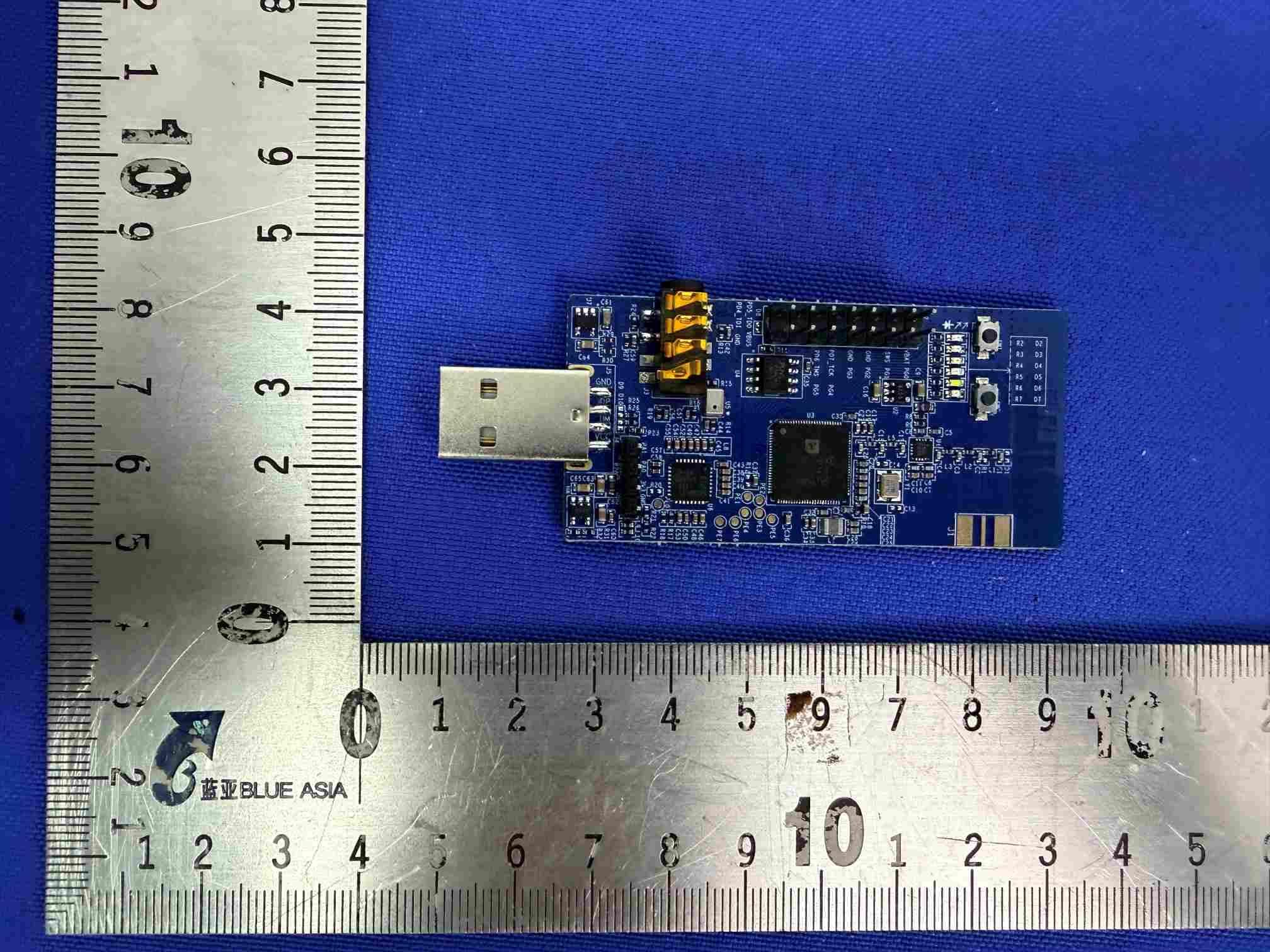
OEOTL3228XDG96D
Jul 14, 2026TL3228XDG96D
Equipment Class
DTS - Digital Transmission System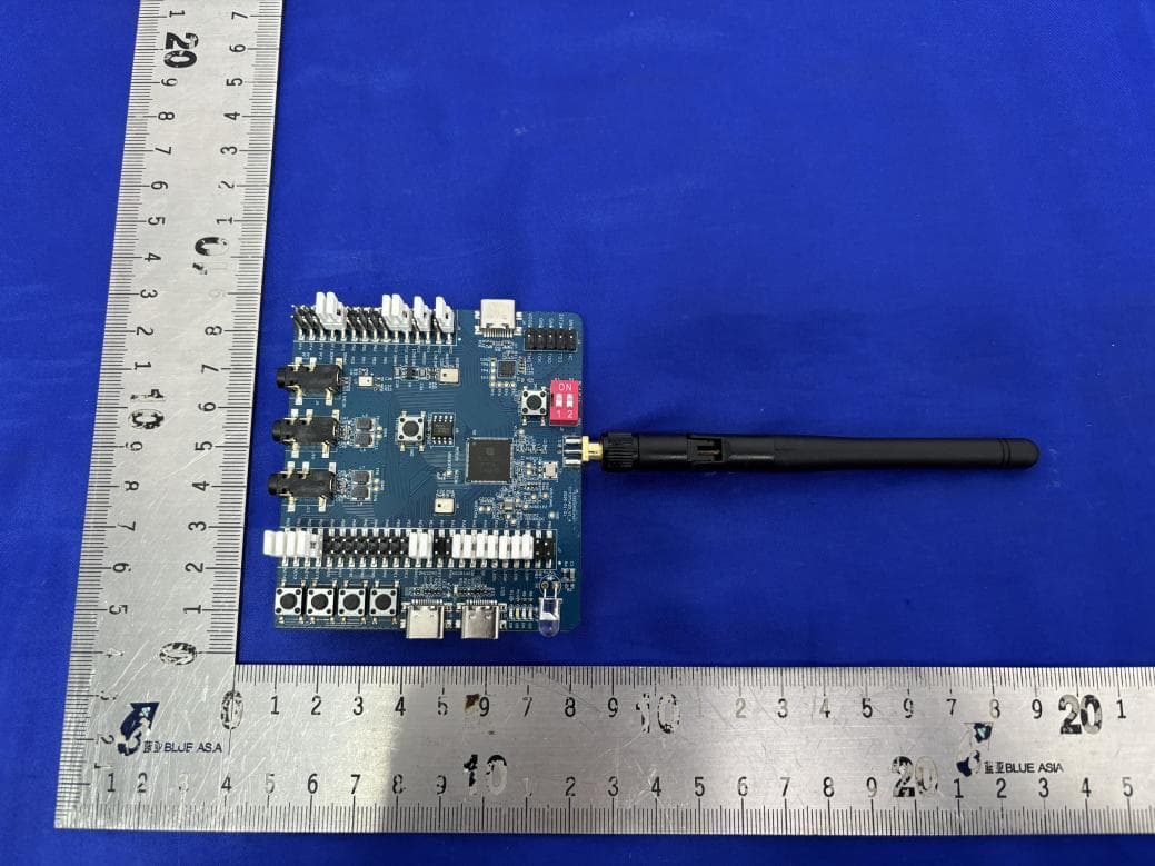
OEOTL3228XDK96D
Jun 01, 2026TL3228XDK96D
Equipment Class
DTS - Digital Transmission SystemOEOM3228AMRM0
Apr 14, 2026ML3228A-GAIA-M3-PE11
Equipment Class
DTS - Digital Transmission System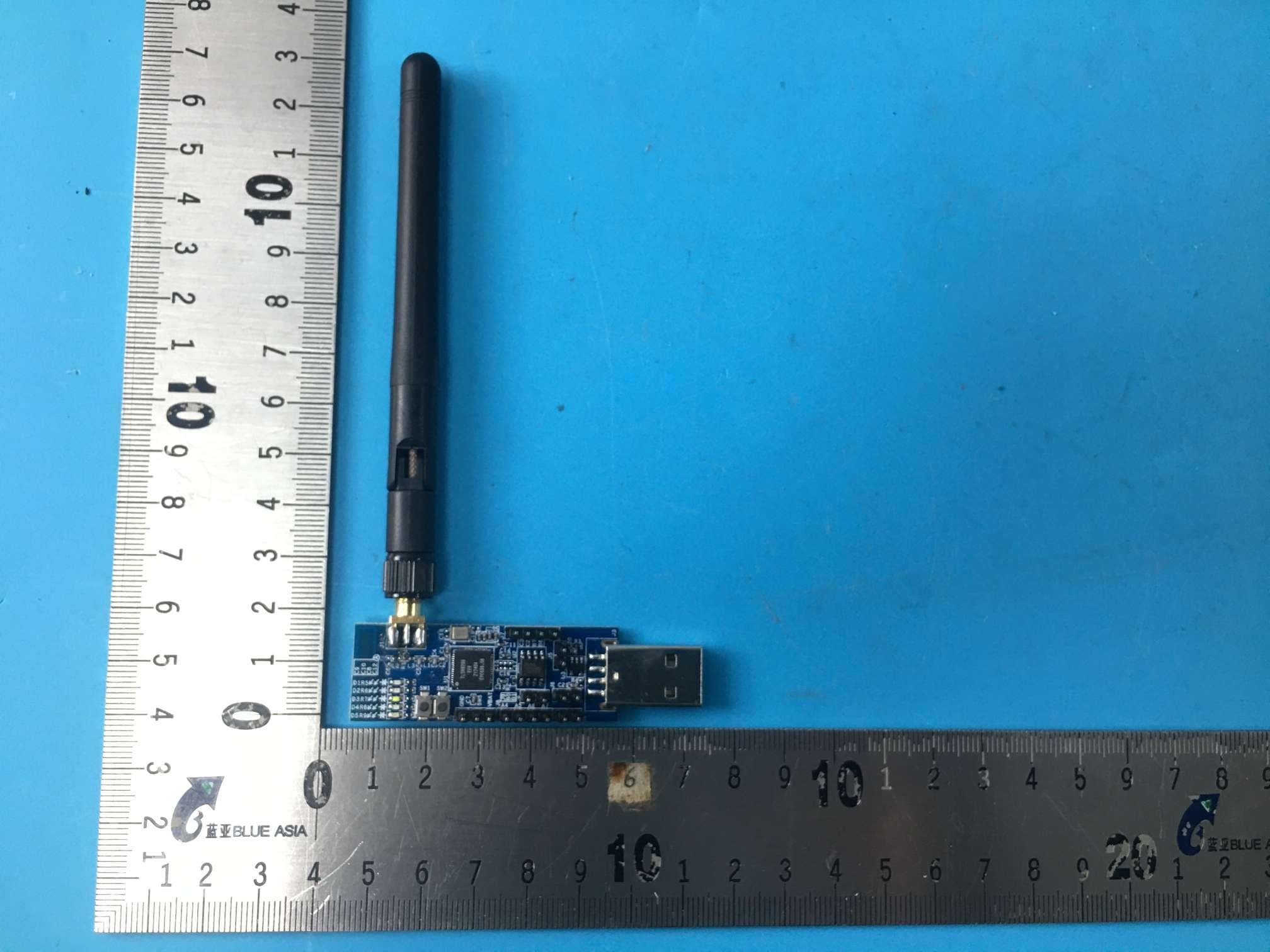
OEOTLSR8208EDG56D
Jun 16, 2024TLSR8208EDG56D
Equipment Class
DTS - Digital Transmission System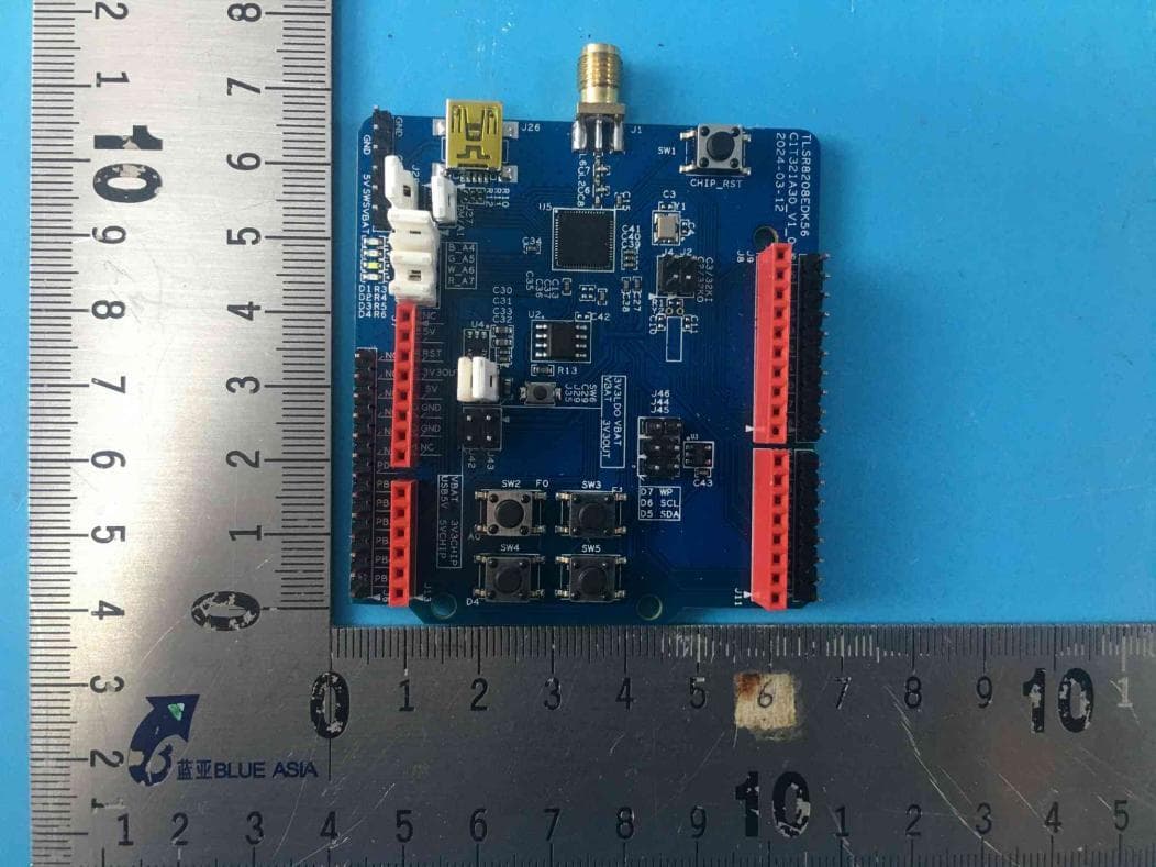
OEOTLSR8208EDK56D
Jun 16, 2024TLSR8208EDK56D
Equipment Class
DTS - Digital Transmission System