OEOTLSR9518ADK80DTLSR9518ADK80D
Telink Semiconductor (Shanghai) Co., Ltd.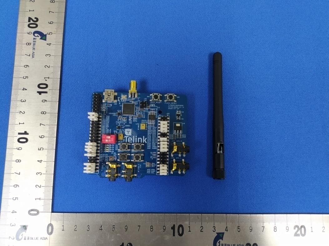
Click to zoom
Application Details
- Equipment Class
- DTS - Digital Transmission System
- Date of Grant
- Sep 15, 2020
- Application Purpose
- Original Equipment
- Date of Application
- Sep 15, 2020
- Equipment Note
- TLSR9518ADK80D
- Frequency Range
- 2402.00000000 - 2480.00000000
- Country
- China
Documents & Files
Document Text
Text extracted from the exhibit documents filed with the FCC. Open a document above to read the original.
Users Manual
Telink Confidential 1 Telink SemiconductorTLSR9518A Generic Starter Kit Hardware Guide 2020-08 Telink Confidential 2 General description General description The guide introduces how to get started with the Kit.TLSR9518A Generic Starter Kit is a hardware platform which can be used to verify TLSR9x series chipset and develop 2.4G protocol application. Telink Confidential 3 Material list The ordering name of TLSR9518A Generic Starter Kit is TLSR9518ADK80D-KIT. Main materials in the kit are listed here. 1x TLSR9518ADK80D - A1x TLSR9 DEV KEY, including DuPont wires - B1x Telink Burning Board, including DuPont wires - C1x USB cable -D1x audio cable, 3.5mm female jack to 2 male 3.5mm audio plug -E 1x audio cable, 3.5mm male plug to 2 male 3.5mm audio plug - F 2x audio cable, 3.5mm audio plug to Canon plug - G2x audio cable, 3.5mm audio plug to Canon jack - H1x Whip Antenna - I Telink Confidential 4 Material list (Cont.) Mini USB D E F B C I G G H H A Telink Confidential 5 Overview The diagram below illustrates main components and default jumper setti ng on TLSR9518ADK80D when user gets it. It supports functions listed here in default setting. RF conducted testExternal Flash with reset buttonChip reset buttonMini USB interface2-wire JTAG, default.4 led, Key matrix up to 4 keys2 line-in function (Dual Analog microphone support ed when switching jumper from microphone path) Dual Digital microphoneStereo line-out Telink Confidential 6 Overview(Cont.) JTAG USB RF SMA CHIP RST FLASH RST TLSR9518A FLASH DMIC KEY MATRIX AMIC AMIC L/R Line ‐ in L/R Line‐out Telink Confidential 7 Power connection method with Telink Burning Board TLSR9518A supports a easy debug meth od. Only three wires are needed. 5V from Telink Burning Board is connected to VBUS from TLSR9518ADK80D. SWM from Telink Burning Board is co nnected to SWS form TLSR9518ADK80D. GND from Telink Burning Board is co nnected to GND form TLSR9518ADK80D. VBUS SWS GND Telink Confidential 8 Power connection method with TLSR9 DEV KEY A RISC-V core is embedded in TLSR951 8A, so TLSR9518A support JTAG debug. The 2x6 connector on the left of mini USB interface is JTAG interface. At th e beginning, user connect TLSR9 DEV KEY to the JTAG interface using DuPont wire s one by one. Then, user can use Telink IDE tool to download FW. Right now, please check if DIP button is under th e right setting. It supports 2-wire JTAG interface when “1” button is on, “2” button is off. On the other side, it supports 4-wire JT AG interface when “1” button is off, “2” button is on. There is a 5V LDO on TLSR9 DEV KEY, so if connecting TLSR9 DEV KEY with TLSR9518ADK80D through DuPont wires, it is not necessary to plug in USB cable. Only when using USB function, user n eed to plug in USB cable. Telink Confidential 9 RF test Power on firstly, then connect RF SMA through cable to equipment or through whip antenna when verifying chipset or develop function. The corresponding tool is EMI tool which can be gotten from wiki. RF Conducted test RF Radiated test Telink Confidential 10 Dual analog microphone function Dual analog microphone function is enable when following the jumper setting as below. Telink Confidential 11 Audio input path test Dual analog microphone function is enable under default setting. When testing audio inpu t path, please change jumper setting as below, the others which are no t showed are kept in their original posi tion. Some audio analyzer can be used for testing, such as APx525. AIR AIL Telink Confidential 12 Audio output path test All jumpers are kept in default setting, and the connection of audio output path is as below. Some audio analyzer can be used for testing, such as APx525. SPK ‐ R SPK ‐ L Telink Confidential 13 Audio input/output path demo Sometimes, user wants to listen to music directly in development stag e. Then, the connection is as below. Earphone Audio Source Telink Confidential 14 GPIO test All of GPIOs of TLSR9518A have been connected to PINs. Then user can ready correspon ding schematic and test all GPIOs. FCC StatementThis device complies with Part 15 of the FCC rules. Operation is subject to the following two conditions: 1)this device may not cause harmful interference, and 2) this device must accept any interference received,including interference that may cause undesired operation.This equipment has been tested and found to comply with the limits for a Class B digital device, pursuant toPart 15 of the FCC rules. These limits are designed to provide reasonable protection against harmfulinterference in a residential installation. This equipment generates, uses and can radiate radio frequencyenergy and if not installed and used in accordance with the instructions, may cause harmful interference toradio communications. However, there is no guarantee that interference will not occur in a particularinstallation. If this equipment does cause harmful interference to radio or television reception, which can bedetermined by turning the equipment off and on, the user is encouraged to try correct the interference by oneor more of the following measures:- Reorient the receiving antenna.- Increase the separation between the equipment and receiver.- Connect the equipment into and outlet on a circuit different from that to which the receiver is connected.- Consult the dealer or an experienced radio/TV technician for help.Changes or modifications not expressly approved by the party responsible for compliance could void yourauthority to operate the equipment. The distance between user and products should be no less than 20cm
Cover Letter(s)
2020/8/28 E quipment Autorisation Division Federal Communications Commission 7 4 35 Oakland Mills Road Columbia, MD 21046 FCC ID: OEOTLSR9518ADK80D Product Name: TLSR9518ADK80D Reau est f。r c。nfidentialitv Pursuant to Sec tions 0.457 and 0.459 of the commissi。ns rules, we he「eby request that the following documents be held confidential: ( List here the documents for which you are seeking confidentiality - for example ... ) • Schematics • Block diagram • Operation description These materials contain trade secrets and proprieta叩informationand are not customarily「eleasedto the public. The public disclosu「e of this informati。n might be harmful to the company and provide unjustified benefits to。ur competitors. <Signature> Name Xiang Ii X,叮 L,' Title Manager Company Telink Semic。『1duct。r (Shanghai) C。.,Ltd.
External Photos
Model No.: TLSR9518ADK80D
ID Label/Location Info
Model No: TLSR9518ADK80D FCC ID: OEOTLSR9518ADK80D Manufacture: Telink Semiconductor (Shanghai) Co., Ltd. Address: Bldg 3, No.1500, Zuchongzhi Rd, Zhangjiang Hi-Tech Park, Shanghai 201203, China Importer: XXX Address: XXX
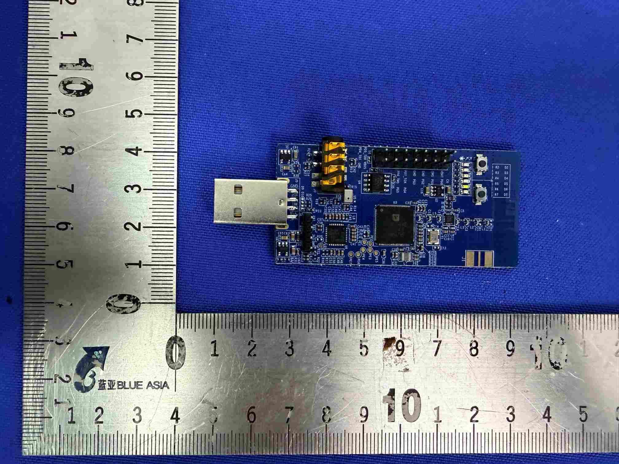
Internal Photos
Model No.: TLSR9518ADK80D
RF Exposure Info
Page 1 of 2 BlueAsia Technology Services(Shenzhen) Limited Add:No. 448, Bulong Road, Bantian Street, Longgang District, Shenzhen, China Tel: +86-755-23059481 Email: [email protected] www.cblueasia.com Product Name: TLSR9518ADK80D Model No.:TLSR9518ADK80D FCC ID:OEOTLSR9518ADK80D RF Exposure Evaluation 1.1 RF Exposure Compliance Requirement 1.1.1 Limits According to FCC Part1.1310: The criteria listed in the following table shall be used to evaluate the environment impact of human exposure to radio frequency (RF) radiation as specified in part1.1307(b) F= Frequency in MHz Friis Formula Friis transmission formula: Pd = (Pout*G)/(4* Pi * R 2) Where Pd = power density in mW/cm2 Pout = output power to antenna in mW G = gain of antenna in linear scale Pi = 3.1416 R = distance between observation point and center of the radiator in cm Pd id the limit of MPE, 1 mW/cm2 . If we know the maximum gain of the antenna and the total power input to the antenna, through the calculation, we will know the distance r where the MPE limit is reached. 1.1.2 Test Procedure Software provided by client enabled the EUT to transmit and receive data at lowest, middle and highest channel individually. Page 2 of 2 BlueAsia Technology Services(Shenzhen) Limited Add:No. 448, Bulong Road, Bantian Street, Longgang District, Shenzhen, China Tel: +86-755-23059481 Email: [email protected] www.cblueasia.com 1.1.3 EUT RF Exposure Evaluation Antenna Gain: 0dBi Antenna Gain: The maximum Gain measured in fully anechoic chamber is 1.000 in linear scale. Output Power Into Antenna & RF Exposure Evaluation Distance: Channel Frequency (MHz) Max Conducted Peak Output Power (dBm) Output Power to Antenna (mW) Power Density at R = 20 cm (mW/cm 2 ) Limit Result Middle 2442 11.56 14.32 0.0028 1.0 PASS Note: Refer to report No. BLA-EMC-202008-A4201 for EUT test Max Conducted Peak Output Power value. The distance r (4th column) calculated from the Fries transmission formula is far greater than 20 cm separation Requirement
Test Report
Page 1 of64 BlueAsia Technology Services(Shenzhen) Limited Add:No. 448, Bulong Road, Bantian Street, Longgang District, Shenzhen, China Tel: +86-755-23059481 Email: [email protected] www.cblueasia.com TEST REPORT Product Name : TLSR9518ADK80D Brand Mark : N/A Model No. : TLSR9518ADK80D FCC ID : OEOTLSR9518ADK80D Report Number : BLA-EMC-202008-A4201 Date of Sample Receipt : 2020/8/11 Date of Test : 2020/8/11 to 2020/8/27 Date of Issue : 2020/8/27 Test Standard : 47 CFR Part 15, Subpart C 15.247 Test Result : Pass Prepared for: TELINK SEMICONDUCTOR (Shanghai) CO, LTD Bldg 3, No.1500, Zuchongzhi Rd, Zhangjiang Hi-Tech Park, Shanghai 201203, China Prepared by: BlueAsia of Technical Services(Shenzhen) Co.,Ltd. IOT Test Centre of BlueAsia No. 448 Bulong Road, Bantian Street, Longgang District, Shenzhen,China TEL: +86-755-28682673 Compiled by: Review by: Approved by: Date: 2020/8/27 Report No.: BLA-EMC-202008-A4201 Page 2 of64 BlueAsia Technology Services(Shenzhen) Limited Tel: +86-755-23059481 Email: [email protected] www.cblueasia.com REPORT REVISE RECORD Version No. Date Description 00 2020/8/27 Original Report No.: BLA-EMC-202008-A4201 Page 3 of64 BlueAsia Technology Services(Shenzhen) Limited Tel: +86-755-23059481 Email: [email protected] www.cblueasia.com TABLE OF CONTENTS 1 TEST SUMMARY ........................................................................................................................................6 2 GENERAL INFORMATION .........................................................................................................................7 3 GENERAL DESCRIPTION OF E.U.T. .........................................................................................................7 4 TEST ENVIRONMENT ................................................................................................................................8 5 TEST MODE ................................................................................................................................................8 6 MEASUREMENT UNCERTAINTY ..............................................................................................................8 7 DESCRIPTION OF SUPPORT UNIT...........................................................................................................9 8 LABORATORY LOCATION .........................................................................................................................9 9 TEST INSTRUMENTS LIST ..................................................................................................................... 10 ANTENNA REQUIREMENT .............................................................................................................................. 13 CONCLUSION ...................................................................................................................................................................... 13 RADIATED SPURIOUS EMISSIONS ............................................................................................................... 14 LIMITS ............................................................................................................................................................................. 14 BLOCK DIAGRAM OF TEST SETUP .................................................................................................................................... 15 PROCEDURE ................................................................................................................................................................... 15 TEST DATA ........................................................................................................................................................................ 17 POWER SPECTRUM DENSITY ....................................................................................................................... 25 LIMITS ............................................................................................................................................................................. 25 BLOCK DIAGRAM OF TEST SETUP .................................................................................................................................... 25 TEST DATA ........................................................................................................................................................................ 25 20DB BANDWIDTH .......................................................................................................................................... 26 BLOCK DIAGRAM OF TEST SETUP .................................................................................................................................... 26 TEST DATA ........................................................................................................................................................................ 26 CONDUCTED PEAK OUTPUT POWER .......................................................................................................... 27 LIMITS ............................................................................................................................................................................. 27 BLOCK DIAGRAM OF TEST SETUP .................................................................................................................................... 27 TEST DATA ........................................................................................................................................................................ 28 CONDUCTED EMISSIONS AT AC POWER LINE (150KHZ-30MHZ) ............................................................. 29 LIMITS ............................................................................................................................................................................. 29 Report No.: BLA-EMC-202008-A4201 Page 4 of64 BlueA…
Text truncated - open the document above for the full version.
Test Setup Photos
Model No.: TLSR9518ADK80D
Contact Information
Applicant
Xiang Li
Test Firm
BlueAsia of Technical Services (Shenzhen)Blue Zheng
[email protected]+86 755-23059481-815
Technical Specifications
| # | Rule Parts | Frequency Range | Power Output |
|---|---|---|---|
| 1 | 15C | 2.40 GHz - 2.48 GHz | 14.32 mW |
Other Applications from Telink Semiconductor (Shanghai) Co., Ltd.
OEOTL3228XDG96D
Jul 14, 2026TL3228XDG96D
Equipment Class
DTS - Digital Transmission System
OEOTL3228XDK96D
Jun 01, 2026TL3228XDK96D
Equipment Class
DTS - Digital Transmission SystemOEOM3228AMRM0
Apr 14, 2026ML3228A-GAIA-M3-PE11
Equipment Class
DTS - Digital Transmission System
OEOTLSR8208EDG56D
Jun 16, 2024TLSR8208EDG56D
Equipment Class
DTS - Digital Transmission System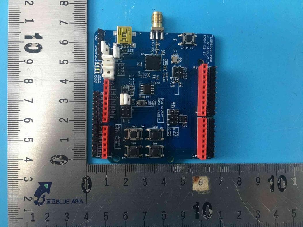
OEOTLSR8208EDK56D
Jun 16, 2024TLSR8208EDK56D
Equipment Class
DTS - Digital Transmission System