OKRMX920Desktop Base Station/Repeater
Spectra Engineering PTY LTD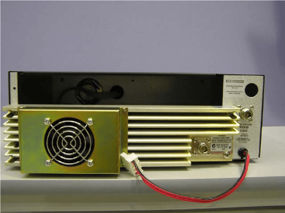
Click to zoom
Application Details
- Equipment Class
- TNB - Licensed Non-Broadcast Station Transmitter
- Date of Grant
- Jun 05, 2004
- Application Purpose
- Original Equipment
- Date of Application
- Jun 05, 2004
- Equipment Note
- Desktop Base Station/Repeater
- Frequency Range
- 485.00000000 - 520.00000000
- Company
- Spectra Engineering PTY LTD
- Country
- Australia
Documents & Files
Document Text
Text extracted from the exhibit documents filed with the FCC. Open a document above to read the original.
Users Manual
OPERATION VOLUME Rotate the volume control clockwise to adjust the volume control for a comfortable listening level. If no sound is heard, temporarily un-mute the radio by briefly rotating the Squelch Control full anti- clockwise. You can adjust the volume by listening to the receiver's background noise. When finished, return squelch setting. (See section on setting Squelch.) CHANNEL SELECTING Push to select the memory channel number for the selected readout. The channel display will Rotate and select the higher channel when the up button is pressed. By pressing the down button the Channel display will rotate to display the lower channel selected. The selected channel is displayed. SQUELCH The squelch is used to eliminate any annoying background noise when there are no signals present. When no signal is received, rotate the Squelch control (SQL) fully counterclockwise first, and then rotate SQL clockwise to the point that the noise just disappears. This will provide optimum Squelch performance. When the Squelch is Open, the receiver's background noise can be heard and 'Green RX LED' is lit on the front panel display. When the Squelch is closed, the receiver remains quiet when there are no signals present but any incoming signals will override the Squelch and be heard in the speaker NOTE: If an incoming signal is very weak and is close to the minimum squelch level, it may become broken or “chopped” by the squelch action. To prevent this, simply open the squelch to allow the signal to be heard clearly. Alternatively, you can reduce the squelch sensitivity as described above. When CTCSS is enabled the channel remains quiet until someone transmits using the same tone. When the transmission ends, the channel becomes quiet again. By using different tones, several groups of people can share the same channel without disturbing each other. ACCESSORY SWITCH The Accessory button is a programmable momentary switch. Which is assigned a function in software programming. (Subject to Radios firmware) See Dealer for application notes for further information on this feature. REPEATER SWITCH This switch enables the MX920 to work as a repeater. In repeater mode, the received signal is processed and retransmits at a different frequency. Repeaters are usually located on hills, mountains or tall buildings. The increased elevation greatly improves the range of the repeater beyond that of a normal base or Mobile. This means that the repeaters are able to receive and retransmit signals to radios that would otherwise be out of range of each other. Receiving A Call With the MX920 powered ‘ON’ the front panel blue led is lit. • Set the audio and squelch levels as per SQUELCH and VOLUME section. • Select the desired receiving channel as per Channel selecting section. • When receiving a signal the ‘Green RX LED‘ indicator lights green when the squelch is open, and audio is emitted from the speaker. • Listen for your call sign when you hear activity, and reply promptly by identifying yourself if called. (For example: Base receiving). Transmitting To Making A Call With the MX920 powered ‘ON’ the front panel blue led is lit. • Select the desired channel, as previously described. • If the ‘Green RX LED' indicator is on, the channel is busy and you must wait until it is free, before proceeding. If you attempt to transmit anyway, the other party may not receive your transmitted signal. • Lift the microphone off-hook and listen to check that no one else is using the channel. You may also have to press the Monitor Key on the desktop Microphone or the Accessory button on the radio briefly, depending on the microphone used and the options programmed to your radio. • When using the Hand-Held microphone, Hold it about 5cm from your mouth and press the Press-To-Talk (PTT) key, located on the side of the microphone (see Figure 3-1). Speak clearly into the microphone at your normal voice level, identifying yourself by your call sign, and the person you wish to contact. (For example: Base to Mobile 2.). • The ‘Red RX LED’ indicator lights while transmitting. • Release the PTT key when you have finished talking. Transmit Timer Your MX920 is fitted with a preprogrammed timer to limit the maximum length of transmissions. When the time limit is reached, the radio sounds a warning tone, and transmission is terminated. (Subject to Radio Firmware) 0 0 0 0 UP CHANNEL UP CHANNEL DOWN CHANNEL DOWN CHANNEL TEN UNITS UNITS PTT PTT Figure 3-1 Figure 3-2 __________________________________________________________________________________________ © SPECTRA ENGINEERING 2004 Revision 1.0.0 INSTALLATION Unpacking The MX920 Radio is securely packed for transport with special end packers within a pasteboard container. Before unpacking the MX920 radio, please inspect the packaging for signs of damage and report any damage to your MX800 distributor. Upon unpacking of the MX920 radio, please ensure that all items shipped were received, report any missing items to your MX920 distributor. All ports on the rear of the radio should be carefully examined to ensure that packaging has not become wedged inside them. It is very important to examine the fan, as operation of the radio will be affected if any packaging or shipping damage causes the fan to stop working. Installing the Base Station System The MX920 is designed to be used in a stand-alone configuration. Ensure that it is in a secure, dry location with sufficient air space around it to allow for adequate ventilation. It is recommended that the chassis be earthed. An optional 19inch rack mount tray is available for mounting the repeater into a 19-inch rack. If you intend to install the radio in an equipment rack consult the suppliers instructions for your system. Power Supply The MX920 has been design to fit an optional internal power supply (PSU). It can also be fitted with optional sealed lead acid batteries Kit for a backup battery. Automatic Backup Battery Change Over System and charger ONLY available in…
Text truncated - open the document above for the full version.
Cover Letter(s)
SPECTRA ENGINEERING PTY LTD ACN 057 696 438 High Performance Base Stations and Repeaters 9 TRADE ROAD MALAGA, 6090. WESTERN AUSTRALIA. TEL: +(61-8) 92482755 FAX: +(61-8) 92482756 Email: [email protected] To: Federal Communications Commission Authorization and Evaluation Division Confidentiality Request regarding application for certification of FCC ID: OKRMX920 Pursuant to Sections 0.457 and 0.459 of the Commission’s Rules, we hereby request confidential treatment of information accompanying this application as outlined below: Schematics and Block Diagrams. The above materials contain trade secrets and proprietary information not customarily released to the public. The public disclosure of these materials may be harmful to the applicant and provide unjustified benefits to its competitors. The applicant understands that pursuant to Section 0.457 of the Rules, disclosure of this application and all accompanying documentation will not be made before the date of the Grant for this application. Sincerely, Gary Jacobs Managing Director Date May 25th, 2004
External Photos
APPENDIX C - EUT EXTERNAL PHOTOGRAPHS Chassis – H_V Plastic Front View Chassis – Horizontal Front View Chassis – Vertical Front View Chassis – Back View Chassis – Horizontal Side View Chassis – Rear View with Cover
ID Label/Location Info
EXHIBIT A – FCC ID LABELING FCC ID Label FCC ID Label Location
Internal Photos
APPENDIX C - EUT INTERNAL PHOTOGRAPHS Chassis – Rear View without Cover Chassis – Top View with Cover Removed EUT – PCB View Complete in Chassis EUT – PCB Top View EUT – PCB Bottom View
Operational Description
Technical Manual 1. Technical Description The internal design of the MX920 is of a modular nature allowing for simple configuration and maintenance while ensuring minimal downtime. 1.1 Exciter Section RF from the VCO is at a nominal level of +3 dBm is applied to the fractional-N synthesiser main divider input. This signal is compared with the reference oscillator frequency and the correction voltage from the synthesiser’s charge pump output is filtered then amplified by an op amp. This correction voltage is fed back to the VCO to maintain loop lock as well as being fed to the Micro Controller. A lock detect signal is also fed to the Micro Controller. Frequency programming data for the exciter is sent to the synthesiser chip from the Micro Controller via a serial data line under the control of the Clock and Strobe lines. A second RF output from the VCO also at +3 dBm is used as the main transmit RF amplifier signal source. The signal is further amplified by a variable gain wide band bipolar amplifier with 40 dB control range and power output of a nominal 300 mW. The drive power of this stage is used to set the output power to the main power amplifier under the control of the DC voltage from the Micro Controller board. The VCO section and synthesiser circuits are the similar for the exciter and receiver sections. The power supply to the VCO uses an 8 volt regulator and active filter for maximum noise rejection. For standard modulation, transmit audio is fed to the conventional point of the VCO varactor. 1.1.1 General Radio Management In addition to analogue signal processing circuitry the Micro Controller section accommodates a microprocessor IC2, a 16 kbyte EEPROM IC1, as well as I/O latches and other miscellaneous circuitry. The Micro Controller is responsible for ensuring that the radio acts as programmed by the user. It stores the user-entered parameters for each channel in EEPROM. This information includes RX and TX RF frequencies; RX and TX CTCSS frequencies as well as RF output power and operating mode. Virtually all logic control is done through the microprocessor. The Micro Controller sends programming data to the synthesiser ICs in the Receiver and Exciter sections each time the channel is changed as well as on PTT. This information is communicated to the Receiver and Exciter sections by way of bussed data and clock lines and an individual module strobe. A lock detect signal from each section is read by the Micro Controller. In addition to the synthesiser programming bus, an I 2 C bus goes to the main EEPROM and PA module EEPROMs. IC29 is a flexible predictive or non-predictive, full duplex CTCSS / Selcall encoder / decoder, DCS decoder, which is under the control of the microprocessor. © SPECTRA ENGINEERING 2003 Revision 1.0.0 1 Technical Manual Installation and Operation 1.1.2 TX Signal Processing TX audio may be sourced from a number of different paths. These include Talk through audio, microphone and tone generators (ie Selcall, DTMF, DCS, CTCSS under micro controller control. The microphone input is feed into a selectable compressor. It is then processed through a preemphasis, summing amp which also serves to combine the audio from the talk through path. Then pass through a HPF filter chain into a gain controlled latch circuit which is under control of microprocessor. The tone generator (Morse code / Selcall) signals from the microprocessor are applied to the input of the limiter amp. Following this the TX VF low pass filter. The standard filter has a 3.4 kHz cut off frequency. A second summing amplifier IC29B follows which combines the reference oscillator centre frequency adjustment and CTCSS level adjustment. The CTCSS signal is fixed to 500Hz deviation for Wide Band channels and 250Hz deviation for Narrow Band (10% of maximum deviation). This level is under microprocessor control (IC24C). The output of this final stage is fed to two microprocessor-controlled digipots, which serve to adjust the modulating signal level to the VCO and the reference oscillator. Adjustment of these levels is by way of the built-in radio configuration menu system using the Channel Edit screen. The MX920 uses the technique of calibrating all Transmit Modulation level alignments in the Wide Band mode (25kHz channel spacing) for maximum accuracy. Gain setting resistor arrays switched under control by the microprocessor automatically scale the levels so as to set the correct modulation depth as required for Narrow Band channels. 1.1.3 RF Power Control Forward power is controlled by the microprocessor through two mechanisms. Based on pre-programmed per channel adjustments the microprocessor sets the digital to analog converter output to a reference setting. IC28B serves as a comparator and, with the non-inverting input connected to the output of the digital to analog converter, is set up with a reference voltage. The detected actual PA forward power is fed to the inverting input of IC28B. The error voltage at the output of IC28B is fed to the exciter output power control circuit via SKB-4 and the action of the control loop is to set the RF power such that the actual detected volts equals the reference volts. The digipot setting is static for each channel unless the required forward power is changed. The voltage to the top of the digipot is set up by the microprocessor through the Pulse Width Modulator output PWM1. On PTT the ON duty cycle of the PWM1 output is progressively increased and the filtered result of this forms a ramp to the top of the power control digipot. Once 100% duty cycle is reached full power is produced. This results in a fast but controlled RF power rise characteristic. 1.1.4 User Interface All user interfaces to the MX920 except the TX RF connections is made by way of the Main Controller board. ♦ Output latch IC4 drives the six LED indicators on the front panel. An input port on IC2 serves to accept the programmed status of the 8-bit BCD channel select input from the front pane…
Text truncated - open the document above for the full version.
Parts List/Tune Up Info
SPECTRA ENGINEERING PTY LTD ABN 65 057 696 438 High Performance Base Stations and Repeaters 9 TRADE ROAD MALAGA, 6090. WESTERN AUSTRALIA. TEL: +(61-8) 92482755 FAX: +(61-8) 92482756 Page 1 of 1 Spectra Part No Designator Description C011 IC4 Octal Buffer/Line Driver C013 IC16 Hex Inverting Schmitt Trigger C015 IC13 RS232 Driver C016 IC6 IC12 Hex Schmitt Trigger C017 IC32 5 Volt Regulator C018 IC19 IC20 IC21 IC23 IC26 IC28 IC33 IC36 DUAL OP AMP C019 IC17 IC22 IC25 IC34 IC35 DUAL OP AMP C021 IC24 IC27 IC41 Quad Analog Switch C024 IC37 8 Volt Regulator C030 IC7 FM IF system IC C034 IC30 Voltage Regulator C052 IC3 IC15 IC39 5 Volt Regulator SMD SO8 C053 IC38 8 Volt Regulator C069 IC8 IC10 QUAD ANALOG SWITCH C089 IC1 CMOS Serial EEprom C091 IC31 BTL Audio amplifier C092 IC29 Rx Audio Processor C093 IC2 Processor C094 IC5 DTMF Processor C095 IC11 IC18 TLC2272CD C097 IC40 M51943 C099 IC9 IC14 N Synthesizer C100 TR25 TR26 RF Cascode Amplifier D002 D11 VARICAP DIODE D003 TR2 TR27 NPN SILICON TRANSISTOR D004 D1D2 D3 D4 D5 D17 D20 DIODE SMD D005 TR18 NPN High Performance Transistors D006 TR21 TRANSISTOR BIPOLAR D007 TR3 TR5 TR6 TR10 TR11 TR14 TR15 TR19 TR20 NPN TRANSISTOR D008 TR17 PNP TRANSISTOR D016 D16 Zener Diode D017 TR16 NPN Wideband transistor D019 D18 D21 D22 D29 DIODE SMD D023 TR13 T751 TRANSISTOR D027 TR9 TR12 J310LT1 D030 D24 LED 3MM AQUA D040 TR24 NPN 9 GHz wideband transistors D041 TR1 TR4 BFS17A D042 D6 Silicon PIN diode D043 D26 LED 3MM YELLOW D047 D27 LED 3MM ORANGE D049 D28 LED 3MM GREEN D050 D23 LED 3MM BLUE D051 D25 LED 3MM RED
Parts List/Tune Up Info
1. Alignment The MX920 test and alignment section assumes that the radio is a working module. Please also see supporting Software Manual for Alignments. 1.1.1 TX Power Adjustment 1.1.2 Peak Deviation and Modulation Balance Alignment This procedure is used to set the peak deviation and modulation balance for each channel. This can be done on a per channel basis or all channels can be set at once. The alignment is done using the Alignment Screen in the built menu system . To carry out this procedure the demodulated output of the transmitter output needs to be connected to a CRO or some other piece of equipment giving a visual display of the demodulated output. IF Bandwidth of the RF test set should be set at 20kHz or greater (230kHz on the HP 8920) and de-emphasise should be off. The audio filters should be set at <20Hz HPF and 15kHz LPF. To alter all channels at once use the ‘Factory default alignment (All Channels). The peak deviation is aligned on wide band and without CTCSS\DCS Tone enabled. The following table specifies the peak deviation to align to. Bandwidth CTCSS Option Peak Deviation (Hz) Wide (25kHz spacing) NO 4800 Table 1-1 Peak Deviation Settings The alignment channel for this routine is the middle frequency band. The test tones used in this routine are generated internally and are a 1 kHz square wave for the transmitter deviation and a 400 Hz square wave for the modulation balance. Procedure: 1. Using in built menu system, select --- ALIGNMENT MENU – 2. Now select either to ‘Align current channel (Individual)’ OR ‘Factory default alignment (All Channels)’ 3. If ‘Align current channel (Individual)’ select Tx Deviation and Modulation Balance - current channel 4. The radio will now transmitter. 5. Follow the built in menu system instructions. 6. The transmitter will be modulated with test frequencies (1kHz, & 400Hz tone generators under micro controller control) 7. Adjust the VCO Deviation digital potentiometer using built menu system until a correct deviation is obtained. (See Table 1-1 Peak Deviation Settings). 8. Adjust the Reference Deviation digital potentiometer until the top of the waveform is flat. If the waveform top droops increase the level (see Figure 1-1) and if it peaks reduce the level (see Figure 1-2). 9. Repeat steps 5 through to 9 until the correct peak deviation and modulation balance is obtained. Examples of incorrect, observed waveforms are as follows: Figure 1-1 Under (increase level) Figure 1-2 Over (decrease level) The waveform when correctly aligned should look as follows: Figure 1-3 Correctly Aligned Waveform Choose ‘OK’ to accept the changes made. This then saves the changes that you have made to the radio. After balancing and setting the correct peak deviation is necessary to align the reference oscillator and re-check the deviation alignment, as the reference oscillator alignment affects the deviation. This may require running through the deviation alignment again after the oscillator alignment procedure. 1.1.3 TX Power & Centre Frequency Alignment The transmitter power setup is used to set the correct power for each channel. This can be done on a per channel basis or all channels can be set at once. The reference oscillator alignment is used to set the correct centre frequency for each channel. This can be done on a per channel basis or all channels can be set at once. Oscillator alignment is done using a digital potentiometer adjustment through the Built in menu system. To carry out this procedure the transmitter output needs to be connected to a RF test set displaying the frequency error and RF power meter. This procedure should be done after the deviation alignment procedure has been done. Transmitter modulation we be disabled. Now select either to ‘Align current channel (Individual)’ OR ‘Factory default alignment (All Channels)’ Select Tx Reference Oscillator and Output Power and follow the in built menus instructions. Alter the Reference Oscillator Frequency potentiometer until the channel is “on frequency”. Choose ‘enter’ to accept the changes made. This then saves the changes that you have made to the radio.
Test Report
Note: This test report is specially limited to the above client company and the product model only. It may not be duplicated without prior written consent of Bay Area Compliance Laboratory Corporation. This report must not be used by the client to claim product endorsement by NVLAP or any agency of the U.S. Government. FCC PART 90 TYPE APPROVAL EMI MEASUREMENT AND TEST REPORT For SPECTRA ENGINEERING PTY LTD 9 Trade Rd Malaga, Perth, Western Australia Australia, 6090 FCC ID: OKRMX920 This Report Concerns: Original Report Equipment Type: Desktop Base Station / Repeater Test Engineer: Benjamin Jin Report No.: R0403267 Report Date: 2004-05-24 Reviewed By: Ling Zhang Prepared By: Bay Area Compliance Laboratory Corporation 230 Commercial Street Sunnyvale, CA 94085 Tel: (408) 732-9162 Fax: (408) 732 9164 Spectra Engineering PTY LTD FCC ID: OKRMX920 Report # R0403267.doc Page 2 of 25 FCC Part 90 Type Approval Report TABLE OF CONTENTS GENERAL INFORMATION.......................................................................................................................................4 PRODUCT DESCRIPTION FOR EQUIPMENT UNDER TEST (EUT) ....................................................................................4 OBJECTIVE...................................................................................................................................................................4 RELATED SUBMITTAL(S)/GRANT(S).............................................................................................................................4 TEST METHODOLOGY..................................................................................................................................................4 TEST FACILITY.............................................................................................................................................................5 SYSTEM TEST CONFIGURATION ..........................................................................................................................6 JUSTIFICATION.............................................................................................................................................................6 BLOCK DIAGRAM.........................................................................................................................................................6 EQUIPMENT MODIFICATIONS.......................................................................................................................................6 TEST SETUP BLOCK DIAGRAM.....................................................................................................................................6 POWER SUPPLY INFORMATION.....................................................................................................................................6 SUMMARY OF TEST RESULTS ...............................................................................................................................7 §2.1046 AND §90.205 - CONDUCTED OUTPUT POWER ......................................................................................8 PROVISION APPLICABLE...............................................................................................................................................8 TEST PROCEDURE........................................................................................................................................................8 TEST EQUIPMENT.........................................................................................................................................................8 ENVIRONMENTAL CONDITIONS....................................................................................................................................8 TEST RESULTS.............................................................................................................................................................8 §2.1047, §90.207 - MODULATION CHARACTERISTIC ........................................................................................9 APPLICABLE STANDARD..............................................................................................................................................9 TEST PROCEDURE........................................................................................................................................................9 TEST EQUIPMENT.........................................................................................................................................................9 ENVIRONMENTAL CONDITIONS....................................................................................................................................9 TEST RESULTS.............................................................................................................................................................9 §2.1049, AND § 90.209 – OCCUPIED BANDWIDTH .............................................................................................12 APPLICABLE STANDARD............................................................................................................................................12 TEST PROCEDURE......................................................................................................................................................12 TEST EQUIPMENT.......................................................................................................................................................13 ENVIRONMENTAL CONDITIONS..................................................................................................................................13 TEST RESULTS...........................................................................................................................................................13 §2.1051 AND §90.210 - SPURIOUS EMISSIONS AT ANTENNA TERMINALS ...........................…
Text truncated - open the document above for the full version.
Contact Information
Applicant
Gary Jacobs(Managing Director)
Test Firm
Bay Area Compliance LaboratoryJohn Chan
Technical Specifications
| # | Rule Parts | Frequency Range | Power Output | Emission | Tolerance |
|---|---|---|---|---|---|
| 2 | 9 | 485 MHz - 520 MHz | 50.23 W | 16K0F9W | 1.5 ppm |
Other Applications from Spectra Engineering PTY LTD
OKRMX800TRV
Nov 22, 2011MX800- Base Station
Equipment Class
TNB - Licensed Non-Broadcast Station Transmitter
OKRMX800WL
Nov 01, 2010MX800- Base Station
Equipment Class
TNB - Licensed Non-Broadcast Station Transmitter
OKRMX800NOPV
Oct 13, 2010MX800- Base Station
Equipment Class
TNB - Licensed Non-Broadcast Station Transmitter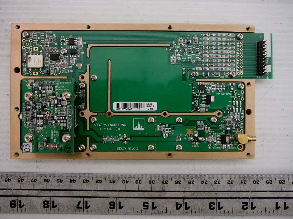
OKRMX800D3V
Oct 11, 2010MX800 - Base Station
Equipment Class
TNB - Licensed Non-Broadcast Station TransmitterOKRMX800R2R3
Jun 26, 2002RF Base Station/Repeater
Equipment Class
TNB - Licensed Non-Broadcast Station Transmitter