OQ3MAF800-100SMulti-Carrier Power Amplifier
Paradigm Wireless Systems Inc
Click to zoom
Application Details
- Equipment Class
- AMP - Amplifier
- Date of Grant
- Jul 25, 2002
- Application Purpose
- Original Equipment
- Date of Application
- Jul 25, 2002
- Equipment Note
- Multi-Carrier Power Amplifier
- Frequency Range
- 869.00000000 - 894.00000000
- Country
- United States
Documents & Files
Document Text
Text extracted from the exhibit documents filed with the FCC. Open a document above to read the original.
Users Manual
REPORT RC055097/28116 APPENDIX A SERVICE/OPERATING MANUAL MAF800-100S MULTI-CARRIER POWER AMPLIFIER USER MANUAL Table Of Contents Page Section 1No. General Description ..............................................................................................................1 Section 2 Specifications ........................................................................................................................2 Section 3 Multi-Carrier Power Amplifier Principals of Operation.......................................................3 Principals of Operation .........................................................................................................4 Principals of Operation .........................................................................................................5 Principals of Operation.............................................................6 Section 4 Operating Instructions...........................................................................................................7 Operating Instructions...............................................................8 Section 5 Installation Instructions.........................................................................................................9 Installation Instructions........................................................................................................10 Installation Instructions........................................................................................................11 Section 6 Maintenance .........................................................................................................................12 Maintenance .........................................................................................................................13 Maintenance .........................................................................................................................14 Maintenance .........................................................................................................................15 Maintenance .........................................................................................................................16 Section 7 Troubleshooting.....................................................................17 1 Section 1 Amplifier System Description 1.1 Introduction This manual contains information and procedures for installation, operation, and maintenance of Paradigm Wireless Systems MAF800-100S multi-carrier cellular amplifier. This manual is organized into the following sections: Section 1. Amplifier System Description Section 2. Specifications Section 3. Principals of Operation Section 4. Operating Instructions Section 5. Installation Section 6. Mainte na nce Section 7. Troubleshooting 1.2 Ge ne ral De script io n The MAF800-100S is a linear, feed forward power amplifier that operates in the 25 MHz frequency range from 869 MHz to 894 MHz. The average output power of the amplifier is 100 Watts average AMPS, CDMA, CDMA 2000, 1xEV-DO, GSM, TDMA, and EDGE. The amplifier is designed to operate in a maximum of two continuous modulations or a total instantaneous bandwidth of 25 MHz. The amplifier can simultaneously transmit multiple frequencies, with a better than –13 dBm third order intermodulation distortion. The amplifier is designed and suited for use in CDMA, TDMA, EDGE and GSM radio base stations. A sub-rack is employed to combine the outputs of up to (4) MAF800-100S amplifiers. Each plug- in module operates in parallel to produce a high peak output power and fail safe redundancy for trouble free operation with mi ni mum mai nte na nce. A mul ti-color LED de tects whe n a faul t condi tion has occ urred within the amplifier. The LED will turn from GREEN to RED during an amplifier fault condition. Each amplifier has a status connector that allows the host system to monitor the amplifier module performance. Monitoring of the amplifiers is done through the D-subminiature connector on the back of the MAF800-100S amplifiers. The front panel of the MAF800-100S amplifier has an ON/OFF circuit breaker. Primary +27 Vdc power for the MAF 800-100S amplifiers is provided through the sub-rack assembly. The sub-rack contains the fan assembly for cooling each amplifier. Cooling fans are used to pull air through the heat sinks. Air movement across the heat sinks dissipates the heat generated by the amplifiers. Constant airflow ensures the amplifiers performance to specifications. Section 2 MAF800-100S Electrical Specification ParameterSpe cificatio n Frequency869-894 MHz RF Gain58 dB Gain Variation over Temperature0.3 dB Gain Flatness0.5 dB Inter mod ulatio n Distortio n ≤ -13 dBm 2 Out o f Ba nd Sp urious ≤ -13 dBm Input Power-4 dBm Output Power100 Watts Modulation TypeAMPS, CDMA, CDMA 2000, TDMA, EDGE, GSM, 1x EV-DO Operating Insta nta neo us Ba ndw idth25 MH z Input Return Loss ≥ 15 dB Output Return Loss ≥ 15 dB Output ProtectionMismatched Protected Duty CycleContinuous Vdc I np ut Pow e r+27 Vdc Operating Current24 amps per amplifier MAF800-100S Environmental Specifications: ParameterSpe cificatio n Operating Temperature 0 ° C. to 50 ° C. Storage Temperature -40 ° C. to + 80 ° C. Operating Humidity5%- 95% Relative Humidity (Non-condensing) Storage Humidity5%-95% Relative Humidity (Non-condensing) RF Input / Output ConnectorD-Sub, Hybrid, Plug-in Type RF Connector: PKZ 26-0020 series straight plug (Phoenix Co.) Status / Alarm / Control / DC Input Connector21 Pin D-Subminiature Combo Connector Di mensio ns Weight Section 3 Principals of Operation 3.1 Introduction This section contains the functional description of the MAF800-100S multi-carrier power amplifier. 3.2 RF Input Signal The maximum composite input power shall not exceed – 4 dBm. The reference source signal shall not exceed the base station manufacture minimum requirements for intermodulation distortion. For proper loop balance, the out of band components of the input sign…
Text truncated - open the document above for the full version.
Block Diagram
MAF800-100S Block Diagram
Cover Letter(s)
From: CERTADM Sent: Thursday, June 27, 2002 6:46 PM To: '[email protected]' Subject: PARADIGM WIRELESS SYSTEMS, INC., FCC ID:OQ3MAF800-100S, AN02T2064 Notice_content ------------- Question #1: Photographs are listed as requested for confidentiality. It is FC C policy not to grant photographs as confidential document. Please rem ove this item and provided revised request for confidentiality letter. Question #2: This device is capable of provide AMPS/CDMA/W-CDMA/1xEV -DO/GSM/TDMA and EDGE modulations. Please provide emission designator for each modulation. Question #3: Test report indicates this amplifi er will be operating under Part 22 and Part 90 of FCC rules. Please sp ecify which services will be provided under Part 90 of FCC rules. Qu estion #4: The items indicated above must be submitted before processin g can continue on the above referenced application. Failure to provide the requested information within 60 days of the original e-mail date ma y result in application dismissal and forfeiture of the filing fee. Als o, please note that partial responses increase processing time and shou ld not be submitted. Any questions about the content of this correspond ence should be directed to the e-mail address listed below the name of the sender.
Cover Letter(s)
From: Bryan Broaddus [[email protected]] Sent: Monday, July 22, 2002 9:24 AM To: [email protected] Cc: [email protected] Subject: RE: Paradigm Emission Designators Mike, Here are the emission designators for the Paradigm unit: AMPS- F1D CDMA- F9W TDMA- DXW EDGE- G7W GSM- GXW 1xEV-DO- F9W Additionally, this unit will only be certified under Part 22 of the FCC rules. If there are any other issues please let me know. Bryan Broaddus DNB Engineering, Inc.
External Photos
FCC ID: OQ3MAF800-100S 14 Photo 13 External Front, Back and Side Views FCC ID: OQ3MAF800-100S 15 Photo 14 External Front, Back and Side Views FCC ID: OQ3MAF800-100S 16 Photo 15 External Front, Back and Side Views
ID Label/Location Info
2.1033 (C) (11)Equipment Identification Plate RF AMPLIFIER MODEL NO. MAF800-100S VOLTAGE: 27 VDC, 24A PWR OUTPUT: 100W FCC ID: OQ3MAF800-100S SERIAL NO.__________ PARADIGM WIRELESS TECHNOLOGY MADE IN USA NOTES: Label will be constructed of 0.02 inch aluminum as shown on the equipment with permanent adhesive. All information on the label will be etched or stamped. Both methods will exceed the expected lifetime of the equipment. The label will be large enough to allow all information to be legible.
Internal Photos
FCC ID: OQ3MAF800-100S 1 2.1033 (C) (11) Equipment Photographs Note: The Main Circuit Board shown in these photos has no components on the reverse side. Photo 1 Main Circuit Board (Overall View Side A) Photo 2 Detail View (Side A) Photo 3 Detail View (Side A) Photo 4 Detail View (Side A) Photo 5 Detail View (Side A) Photo 6 Detail View (Side A) Photo 7 Overall View (Side B) Photo 8 Detail View (Side B) Photo 9 Detail View (Side B) Photo 10 Detail View (Side B) Photo 11 Detail View (Side B) Photo 12 Detail View (Side B) Photo 13 External Front, Back, and Side Views Photo 14 External Front, Back, and Side Views Photo 15 External Front, Back, and Side Views FCC ID: OQ3MAF800-100S 2 Photo 1 Main Circuit Board (Overall View Side A) FCC ID: OQ3MAF800-100S 3 Photo 2 Detail View (Side A) FCC ID: OQ3MAF800-100S 4 Photo 3 Detail View (Side A) FCC ID: OQ3MAF800-100S 5 Photo 4 Detail View (Side A) FCC ID: OQ3MAF800-100S 6 Photo 5 Detail View (Side A) FCC ID: OQ3MAF800-100S 7 Photo 6 Detail View (Side A) FCC ID: OQ3MAF800-100S 8 Photo 7 Overall View (Side B) FCC ID: OQ3MAF800-100S 9 Photo 8 Detail View (Side A) FCC ID: OQ3MAF800-100S 10 Photo 9 Detail View (Side B) FCC ID: OQ3MAF800-100S 11 Photo 10 Detail View (Side B) FCC ID: OQ3MAF800-100S 12 Photo 11 Detail View (Side B) FCC ID: OQ3MAF800-100S 13 Photo 12 Detail View (Side B)
Operational Description
Section 3 Principals of Operation 3.1 Introduction This section contains the functional description of the MAF800-100S multi-carrier power amplifier. 3.2 RF Input Signal The maximum composite input power shall not exceed – 4 dBm. The reference source signal shall not exceed the base station manufacture minimum requirements for intermodulation distortion. For proper loop balance, the out of band components of the input signal shall not exceed –40 dBc. The input VSWR should be 2:1 maximum 3.3 RF Output Load The load impedance should be equal to or better than 1.5:1 in the operating band for good power transfer to the load. If the amplifier is operated into a filter, it will ma intain its distortion characteristics outside the signal band even if the VSWR is infinite. Provided the reflected power does not exceed one-watt. A parasitic signal of less than one-watt incident on the output will not cause distortion at a higher level than the normal forward distortion 3.4 Amplifier Functional Description The MAF800-100S amplifier is a linear, feed-forward power amplifier that operates in the 25 MHz frequency band from 869 MHz -894 MHz. The amplifier is designed to operate in an instantaneous bandwidth of 25 MHz. Each amplifier is a self-contained plug in module and is functionally independent of the other amplifier module. The amplifier modules are designed for parallel operation to achieve high peak power output, and for redundancy in unmanned remote locations. Each amplifier in the system can simultaneously transmit multiple carrier frequencies, at an average total power output of 100 Watts, with better than –13 dBm intermodulation distortion. All phase and gain corrections are performed on the signal (s) in the individual amplifier module. Each amplifier module has an alarm board that monitors the amplifier performance. If a failure or fault occurs in the amplifier module a multi-color LED will change from GREEN to RED. This will be displayed on the front of the individual amplifier front panel. 3.5 MAF800-100S Amplifier Module The amplifier module has an average output of 100 Watts power with intermodulation products suppressed to better than -13 dBm. The amplifier provides an amplified output signal with constant gain and phase by adding approximately 25 dB of distortion cancellation on the output signal. Continuously comparing active paths with passive references, and correcting for small variations through RF feedback control maintain constant gain and phase. The amplifier module is comprised of: Preamplifiers Main Amplifiers Error Amplifier Two feed-forward loops with phase–shift and gain controls DC/DC power regulator Alarm monitoring, control and LED display lamp MAF800-100S Block Diagram The main amplifier employs class AB amplification for maximum efficiency. The error amplifier and feed forward loops are employed to correct signal non-linearity introduced by the class AB main amplifier. The error amplifier operates in class AB mode. The RF input signals are amplified by a preamp and coupled to an attenuator and phase shifted by 180 degrees and amplified in the pre-main amplifier. The output from the pre-main amplifier is fed to the class AB ma in amplifier. The output from the main amplifier is typically 100 Watts. The signal output from the main amplifier is sampled using a coupler. The sample signal is combined with the main input signal and input to the second feed-forward loop. The error signal is attenuated, phase shifted 180 degrees, then passed to the error amplifier where it is amplified to a level identical to the sampled output from the main amplifier. The output from the error amplifier is then coupled back and added to the output from the main amplifier. The control loops continuously make adjustments to cancel out any distortion in the final output signals. The primary function of the 1 st loop is to provide an error signal for the 2 nd loop. The primary function of the 2 nd loop is to amplify the error signal to cancel out spurious products developed in the main amplifier. The input signal is amplified by a pre-amplifier and fed to a coupler and delay line. The signal from the coupler is fed to the attenuator and phase shifter in the 1 st loop. The 1 st loop control section phase shifts the main input signals by 180 degrees and constantly monitors the output for correct phase and gain. The 2 nd loop control section obtains a sample of the distortion added to the output signals by the main amplifiers, and then phase shifts the signals by 180 degrees then feeds the signal to the error amplifier. There it is amplified to the same power level as the input sample and coupled on to the main output signal. The final output is monitored by the 2 nd loop and adjusted to ensure that the signal distortion and IMD on the final output is cancelled. 3.6 Main Amplifier The input and output of the amplifier employ two-stage, class AB amplifiers, which provide approximately 25 dB of gain in the 25 MHz frequency band, from 869 MHz to 894 MHz. The amplifier operates on +27 Vdc, and is mounted directly on a heat sink, which is temperature monitored by a thermal sensor. If the heat sink temperature exceeds 85° C. a high temperature fault occurs. The alarm logic controls the transistor bias voltage; this shuts down the amplifier if bias voltage is out of range. 3.7 Error Amplifier The primary function of the error amplifier is to sample and amplify the signal distortion level generated by the main amplifier. The error amplifier cancels out the distortion and IMD when the error signal is coupled onto the main signal at the amplifier output. The matching signa l levels from the error amplifier are injected back into the main amplifier output reducing any distortion and cancellation of IMD. The error amplifier is a balanced multistage class AB amplifier. It has 75 dB of gain, and produces up to 65 Watt output. The amplifier operates on +27 Vdc and is mounted directly on a heat sink. 3.8 Amplifi…
Text truncated - open the document above for the full version.
Test Report
FCC ID: OQ3MAF800-100S 1 Application for Certification For an RF Power Amplifier Paradigm Wireless Systems Inc. 1672 McGaw Ave. Irvine, CA 92614 RF Power Amplifier: Part # MAF800-100S FCC ID: OQ3MAF800-100S REPORT # RC055097/28116 This report was prepared in accordance with the requirements of the FCC Rules and Regulations Part 2, Subpart J, 2.1031 through 2.1057, Part 22 and Part 90 and other applicable sections of the rules as indicated herein. Prepared By: Fred Gurule DNB Engineering, Inc. 3535 W. Commonwealth Ave. Fullerton, CA 92833 30 MAY 2002 FCC ID: OQ3MAF800-100S 2 FCC ID: OQ3MAF800-100S 3 TABLE OF CONTENTS Section Title Sheet # 1.0ADMINISTRATIVE DATA3 1.1Certificatio ns a nd Q ua lificatio ns3 1.2Meas ure me nts a nd Repea tab ility Info rma tio n3 Note: Paragraph numbers in this report follow the application section numbers found in the FEDERAL COMMUNICATIONS COMMISSION Rules and Regulations, Part 2, Subpart J for Certification of electronic equipment. 2.1033 (C) (1)Application for Certification4 2.1033 (C) (2)FCC Identifier4 2.1033 (C) (3)Installation and Operating Instructions4 2.1033 (C) (4)Type of Emissions4 2.1033 (C) (10)Schematic Diagram and C ircuit Description5 2.1033 (C) (11)Equipment Identification Plate5 2.1033 (C) (12) Equipment Photographs6 - 15 2.1033 (C) (13)Digital Modulation Techniques22 2.1033 (C) (14)Test Data22 2.1033 (C) (5)Frequency Range25 2.1033 (C) (6)Operating Power25 2.1033 (C) (7)Maximum Power Allowed in Applicable part(s) of the Rules25 2.1033 (C) (8)Final RF Amplifier Input Power C haracteristics25 2.1033 (C) (9)Tune Up Procedure25 2.1046Measurement of RF Power Output22 2.1049Measurement of Occupied Bandwidth23 FIGURE 1 :BLOCK DIAGRAM (Occ up ied Ba nd wid th te sts )24 2.1051Spurious Emissions at Antenna Terminals26 FIGURE 2: BLOCK DIAGRAM (Spurious Emissions tests)27 2.1053Measurement of Field Strength of Spurious Radiation28 Table 1: Field Strength of Spurious RadiationData Pkgs Test Equipment Log29 - 30 2.1055Measurement of Frequency Stability31 2.1057Frequency Spectrum to be Investigated31 APPENDIX AService/Operating ManualA1 - A18 APPENDIX BSchematicsB1 – B8 DATA PACKAGESPlots and Data for each Modulation Condition(7 Pkgs) FCC ID: OQ3MAF800-100S 4 1.0ADMINISTRATIVE DATA 1.1Certifications and Qualifications I certify that DNB Engineering, Inc conducted the tests performed in order to obtain the technical data presented in this application. Also, based on the results of the enclosed data, I have concluded that the equipment tested meets or exceeds the requirements of the Rules and Regulations governing this application. 1.2Measurement Repeatability Information The test data presented in this report has been acquired using the guidelines set forth in FCC Part 2.1031 through 2.1057, Part 22 and Part 90. The test results presented in this document are valid only for the equipment identified herein under the test conditions described. Repeatability of these test results will only be achieved with identical measurement conditions. These conditions include: The same test distance, EUT Height, Measurement Site Characteristics, and the same EUT System Components. The system must have the same Interconnecting Cables arranged in identical placement to that in the test set-up, with the system and/or EUT functioning in the identical mode of operation (i.e. software and so on) as on the date of the test. Any deviation from the test conditions and the environment on the date of the test may result in measurement repeatability difficulties. All changes made to the EUT during the course of testing as identified in this test report must be incorporated into the EUT or identical models to ensure compliance with the FCC regulations. Bryan Broaddus (Para. 1.1) Manager, Test Dept. DNB Engineering, Inc. Tel. (714) 870-7781 FAX (714) 870-5081 FCC ID: OQ3MAF800-100S 5 2.1033 (C) (1)Application for Certification Name of Applicant:Paradigm Wireless Systems Inc. 1672 McGaw Ave. Irvine, CA 92614 Applicant is:XManufacturer Vendor Licensee Prospective Licensee Other Name of ManufacturerParadigm Wireless Technology Description: RF Power Amplifier Part Number: MAF800-100S Anticipated Production Quantity: Multiple Units 2.1033 (C) (2)FCC Identifier FCC ID: OQ3MAF800-100S 2.1033 (C) 3)Installation and Operating Instructions Please refer to Appendix A 2.1033 (C) (4)Type of Emission N/A (CDMA Modulation) FCC ID: OQ3MAF800-100S 6 2.1033 (C) (10)Schematic Diagram and Circuit Description Please refer to Appendix B 2.1033 (C) (11)Equipment Identification Plate RF AMPLIFIER MODEL NO. MAF800-100S VOLTAGE: 27 VDC, 24A PWR OUTPUT: 100W FCC ID: OQ3MAF800-100S SERIAL NO.__________ PARADIGM WIRELESS TECHNOLOGY MADE IN USA NOTES: Label will be constructed of 0.02 inch aluminum as shown on the equipment with permanent adhesive. All information on the label will be etched or stamped. Both methods will exceed the expected lifetime of the equipment. The label will be large enough to allow all information to be legible. FCC ID: OQ3MAF800-100S 7 2.1033 (C) (11) Equipment Photographs Note: The Main Circuit Board shown in these photos has no components on the reverse side. Photo 1Main Circuit Board (Overall View Side A) Photo 2Detail View (Side A) Photo 3Detail View (Side A) Photo 4Detail View (Side A) Photo 5Detail View (Side A) Photo 6Detail View (Side A) Photo 7Overall View (Side B) Photo 8Detail View (Side B) Photo 9Detail View (Side B) Photo 10Detail View (Side B) Photo 11Detail View (Side B) Photo 12Detail View (Side B) Photo 13External Front, Back, and Side Views Photo 14External Front, Back, and Side Views Photo 15External Front, Back, and Side Views FCC ID: OQ3MAF800-100S 8 Photo 1Main Circuit Board (Overall View Side A) Confidential FCC ID: OQ3MAF800-100S 9 Photo 2Detail View (Side A) Confidential FCC ID: OQ3MAF800-100S 10 Photo 3Detail View (Side A) Confidential FCC ID: OQ3MAF800-100S 11 Photo 4Detail View (Side A) Confidential FCC ID: OQ3MAF800-100S 12 Photo 5Detail View (Side A) Confi…
Text truncated - open the document above for the full version.
Test Report
RC055097/28116 1 Data Package 1 Unmodulated Test Data RC055097/28116 2 RC055097/28116 3 RC055097/28116 4 RC055097/28116 5 RC055097/28116 6 RC055097/28116 7 RC055097/28116 8 RC055097/28116 9 RC055097/28116 10 RC055097/28116 11 RC055097/28116 12 RC055097/28116 13
Test Report
RC055097/28116 1 Data Package 2 CDMA IS-95A Modulated Test Data RC055097/28116 2 RC055097/28116 3 RC055097/28116 4 RC055097/28116 5 RC055097/28116 6 RC055097/28116 7 RC055097/28116 8 RC055097/28116 9 RC055097/28116 10 RC055097/28116 11 RC055097/28116 12 RC055097/28116 13
Test Report
RC055097/28116 1 Data Package 3 CDMA 2000 Modulated Test Data RC055097/28116 2 RC055097/28116 3 RC055097/28116 4 RC055097/28116 5 RC055097/28116 6 RC055097/28116 7 RC055097/28116 8 RC055097/28116 9 RC055097/28116 10 RC055097/28116 11 RC055097/28116 12
Test Report
RC055097/28116 1 Data Package 5 GSM Modulated Test Data RC055097/28116 2 RC055097/28116 3 RC055097/28116 4 RC055097/28116 5 RC055097/28116 6 RC055097/28116 7 RC055097/28116 8 RC055097/28116 9 RC055097/28116 10 RC055097/28116 11 RC055097/28116 12
Test Report
RC055097/28116 1 Data Package 6 EDGE Modulated Test Data RC055097/28116 2 RC055097/28116 3 RC055097/28116 4 RC055097/28116 5 RC055097/28116 6 RC055097/28116 7 RC055097/28116 8 RC055097/28116 9 RC055097/28116 10 RC055097/28116 11 RC055097/28116 12
Test Report
RC055097/28116 1 Data Package 7 1XEV-DO Modulated Test Data RC055097/28116 2 RC055097/28116 3 RC055097/28116 4 RC055097/28116 5 RC055097/28116 6 RC055097/28116 7 RC055097/28116 8 RC055097/28116 9 RC055097/28116 10 RC055097/28116 11 RC055097/28116 12
Contact Information
Applicant
Gallin Chen(VP of Business Development)
Test Firm
DNB Engineering, Inc.Clay Allred
Technical Specifications
| # | Rule Parts | Frequency Range | Power Output | Emission | Tolerance |
|---|---|---|---|---|---|
| 5 | 22.901(d) | 869 MHz - 894 MHz | 100 W | GXW | Amp |
Other Applications from Paradigm Wireless Systems Inc

OQ3MAF900-60S
Nov 15, 2001RF Amplifier. M/N:MAF900-60S
Equipment Class
AMP - Amplifier
OQ3MAP800-70S
Aug 05, 2001RF Power Amplifier
Equipment Class
AMP - Amplifier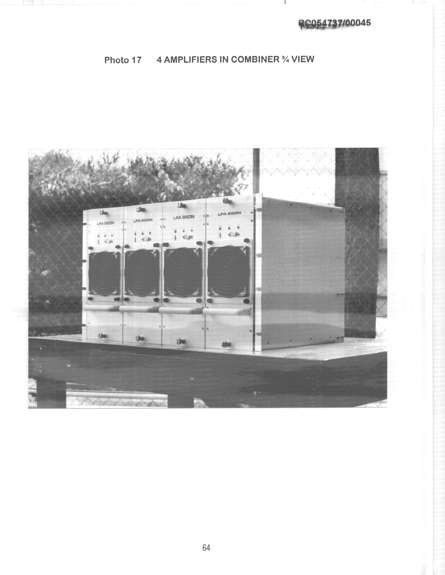
OQ3MS800-200
Mar 22, 2000AMP - Amplifier
Equipment Class
AMP - Amplifier