OUS836A2000-Watt UHF Translator
UBS-Axcera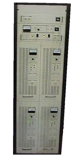
Click to zoom
Application Details
- Equipment Class
- TBC - Licensed Broadcast Station Transmitter
- Date of Grant
- Dec 03, 2002
- Application Purpose
- Original Equipment
- Date of Application
- Oct 13, 2002
- Equipment Note
- 2000-Watt UHF Translator
- Frequency Range
- 470.00000000 - 860.00000000
- Company
- UBS-Axcera
- Country
- United States
Documents & Files
Document Text
Text extracted from the exhibit documents filed with the FCC. Open a document above to read the original.
Users Manual
INSTRUCTION MANUAL 836A 2000 WATT UHF TRANSLATOR AXCERA, LLC 103 FREEDOM DRIVE P.O. BOX 525 LAWRENCE, PA 15055-0525 USA (724) 873-8100 • FAX (724) 873-8105 www.axcera.com • [email protected] 836A 2 kW UHF Television Translator, Internally DiplexedTable of Contents - Page 1 of 2 - 1.Introduction: 2.System - 836A: A.System Description B.Specifications C.Site Considerations D.Unpacking and Installation Procedures E.Translator Set Up and Operation Procedure F.Meters, Switches and Indicators G.Translator Detailed Alignment Procedure H.Remote Control Interface Connections I.Drawings: 1.2 kW Translator Block Diagram.....................................................1276-3000 2.2 kW Translator Interconnect......................................................1276-8000 3.Remote Interface Assembly w/Moseley Interconnect........................1276-8011 3.AC Distribution Assembly, Narrow A.Drawings: 1.Interconnect............................................................................1276-8200 4.UHF Exciter A.Drawings: 1.Block Diagram...........................................................................1265-3300 2.Interconnect............................................................................1265-8300 5.VHF/UHF Receiver Tray A.Drawings 1.Block Diagram...........................................................................1265-3100 2.Interconnect............................................................................1265-8100 6.UHF Amplifier Tray A.Drawings: 1.Block Diagram...........................................................................1281-3100 2.Interconnect............................................................................1281-8100 7.Subassemblies: Refer to the Subassembly Section of the Instruction Manual for the Schematics, of the Boards and Modules that make up the 836A. A Subassembly Drawing List, which is a list of the drawings in the order they appear in the Section, is located in the front of the Subassembly Section. 836A 2 kW UHF Television Translator, Internally DiplexedTable of Contents - Page 2 of 2 - 8.Maintenance: This section contains information on the operation and maintenance of the 836A. This section contains information on the Plugs, Jacks, Sockets and Pins that make up the Harness and Cable Assemblies in the 836A. FF WARNING!!! ◊◊ HIGH VOLTAGE ÿÿ DO NOT ATTEMPT TO REPAIR OR TROUBLESHOOT THIS EQUIPMENT UNLESS YOU ARE FAMILIAR WITH ITS OPERATION AND EXPERIENCED IN SERVICING HIGH VOLTAGE EQUIPMENT. LETHAL VOLTAGES ARE PRESENT WHEN POWER IS APPLIED TO THIS SYSTEM. IF POSSIBLE, TURN OFF POWER BEFORE MAKING ADJUSTMENTS TO THE SYSTEM. ́ ́ RADIO FREQUENCY RADIATION HAZARD ́ ́ MICROWAVE AMPLIFIERS AND TUBES GENERATE HAZARDOUS RF RADIATION WHICH CAN CAUSE SEVERE INJURY INCLUDING CATARACTS, WHICH CAN RESULT IN BLINDNESS. SOME CARDIAC PACEMAKERS MAY BE AFFECTED BY THE RF ENERGY EMITTED BY MICROWAVE AMPLIFIERS. NEVER OPERATE A MICROWAVE SYSTEM WITHOUT A PROPERLY MATCHED RF ENERGY ABSORBING LOAD ATTACHED. KEEP PERSONNEL AWAY FROM OPEN WAVEGUIDES AND ANTENNAS. NEVER LOOK INTO AN OPEN WAVEGUIDE OR ANTENNA. MONITOR ALL PARTS OF THE RF SYSTEM FOR RADIATION LEAKAGE AT REGULAR INTERVALS. EMERGENCY FIRST AID INSTRUCTIONS Personnel engaged in the installation, operation, or maintenance of this equipment are urged to become familiar with the following rules both in theory and practice. It is the duty of all operating personnel to be prepared to give adequate Emergency First Aid and thereby prevent avoidable loss of life. RESCUE BREATHING 1. Find out if the person is breathing. You must find out if the person has stopped breathing. If you think he is not breathing , place him flat on his back. Put your ear close to his mouth and look at his chest. If he is breathing you can feel the air on your cheek. You can see his chest move up and down. If you do not feel the air or see the chest move, he is not breathing. 2. If he is not, open the airway by tilting his head backwards. Lift up his neck with one hand and push down on his forehead with the other. This opens the airway. Sometimes doing this will let the person breathe again by himself. If is does not, begin rescue breathing. 3. If he is still not breathing, begin rescue breathing. -Keep his head tilted backward. Pinch nose shut. -Put your mouth tightly over his mouth. -Blow into his mouth once every five seconds -DO NOT stop rescue breathing breathing until help comes. LOOSEN CLOTHING - KEEP WARM Do this when the victim is breathing by himself or help is available. Keep him as quiet as possible and from becoming chilled. Otherwise treat him for shock. BURNS SKIN REDDENED: Apply ice cold water to burned area to prevent burn from going deeper into skin tissue. Cover area with clean sheet or cloth to keep away air. Consult a physician. SKIN BLISTERED OR FLESH CHARRED: Apply ice cold water to burned area to prevent burn from going deeper into skin tissue. Cover area with clean sheet or cloth to keep away air. Treat victim for shock and take to hospital. EXTENSIVE BURN - SKIN BROKEN: Cover area with clean sheet or cloth to keep away air. Treat victim for shock and take to hospital. LIMITED WARRANTY ONE YEAR Seller warrants each new product manufactured and sold by Seller against defects in material and workmanship under normal use and service, for a period of one (1) year from the date of shipment from Seller's plant, when operated in accordance with Seller's operating instructions. This warranty shall not apply to tubes, fuses, batteries, or bulbs. Warranties are valid only when and if (a) Seller receives prompt written notice of breach within the period of warranty, (b) the defective product is properly packed and returned by the Buyer (transportation and insurance prepaid), and (c) Seller determines, in its sole judgment, that the product is defective and not subject to any misuse, neglect, improper installation, negligence, accident, or (unless authorized in writing by Seller) repair or alteration. Seller'…
Text truncated - open the document above for the full version.
External Photos
Axcera-836A FCC Type Acceptance Report External Photos October 2002 2-1 2. EXTERNAL PHOTOS 2.1 Front view, complete Axcera-836A Translator Axcera-836A FCC Type Acceptance Report External Photos October 2002 2-2 2.2 Rear view, complete Axcera-836A Translator
ID Label/Location Info
Axcera-836A FCC Type Acceptance Report ID Label/Location Info October 2002 1-1 1. ID LABEL/LOCATION INFO 1.1 Rear Panel FCC Label (Translator) 1.2 Rear Panel Manufacturer’s Label (Translator) Axcera-836A FCC Type Acceptance Report ID Label/Location Info October 2002 1-2 1.3 Front view, complete Axcera-836A Translator Axcera-836A FCC Type Acceptance Report ID Label/Location Info October 2002 1-3 1.4 Rear view, Axcera-836A Translator with FCC Label 1.5 Rear view, Axcera-836A Translator with Manufacturer’s Label
Internal Photos
Axcera-836A FCC Type Acceptance Report Internal Photos September 2002 6-1 6. INTERNAL PHOTOS 6.1 Top view, UHF Exciter Tray Axcera-836A FCC Type Acceptance Report Internal Photos September 2002 6-2 6.2 Side view, UHF Amplifier Tray (left side) 6.3 Side view, UHF Amplifier Tray (right side) Axcera-836A FCC Type Acceptance Report Internal Photos September 2002 6-3 6.4 Top view, Receiver Tray
Operational Description
Axcera-836A FCC Type Acceptance Report Operational Description October 2002 8-1 8. OPERATIONAL DESCRIPTION - MODEL Axcera-836A 8.1 General Description The 836A is a complete 2000-watt UHF solid-state, internally diplexed television translator. It operates at a nominal visual output power of 2000 watts peak sync and an average aural output power of 200 watts, at an A/V ratio of 10 dB, 10% sound. 8.2 Technical Specifications Type of Emissions: Visual .......................................................................... 5M75C3F Aural ............................................................................250KF3E Frequency Range....................... 470 MHz to 860 MHz (any 6-MHz channel) Output Power Visual .........................................................2000 watts peak sync Aural .............................................................. 200 watts average Maximum Power Rating Visual ....................................................... 2000 watts peak visual Aural ...................................................... 200 watts average aural Power Consumption .............................................................. 7000 watts 8.3 Performance Specifications Visual Performance Operating Frequency Range ...................................... 470 MHz to 860 MHz RF output - Nominal: Power .........................................................2000 watts peak sync Impedance .................................................................... 50 ohms Connector..................................................................... 7/8" EIA Visual Sideband Response: -1.25 MHz and below ........................................................... -20B -0.75 to -0.5 MHz..................................................... +0.5, -2.0dB -0.5 MHz to +3.58 MHz....................................................±0.5 dB 3.58 MHz to 4.18 MHz.............................................. +0.5, -1.0 dB Variation of Frequency Response with Brightness...........................±0.5 dB Differential Phase ............................................................................ ±3° Incidental Phase Modulation.............................................................. ±3° Differential Gain .............................................................................. 5% Low Frequency Linearity ................................................................... 5% Intermodulation Products .............................................. -52 dB (red field) Output Variation (Over 1 Frame) ....................................................... 2% Regulation of Output........................................................................ 3% Signal-to-Noise Ratio ................................................................. 55 dB Axcera-836A FCC Type Acceptance Report Operational Description October 2002 8-2 2t K-Factor.................................................................................. 2% Harmonic Radiation .....................................................................-60 dB Spurious (>3 MHz from channel edge) ...........................................-60 dB Carrier Frequency Stability........................................................... ±1 kHz Noise Figure w/Input Preamp .................................................3 dB (Max.) Input Dynamic Range (no Preamp) ................................... -60 to -15 dBm Aural Performance RF Output – Nominal Power......................................................................... 200 watts Impedance .................................................................... 50 ohms Connector..................................................................... 7/8" EIA Electrical Requirements Power Line Voltage................................................... 230 volts, 50/60 Hz Power Consumption .............................................................. 7000 watts Environmental Maximum Altitude ..................................................................8,500 feet Operational Temperature Range ........................................-30°C to +50°C Mechanical Dimensions: Width ..........................................................................22 inches Depth ..........................................................................34 inches Height..........................................................................76 inches Weight ............................................................................ 750 lbs 8.4. System Overview The 836A (1276-1000) is made up of the (2) trays listed in Table 8-1. Table 8-1. 836A Major Trays and Assemblies MAJOR ASSEMBLY DESIGNATOR TRAY/ASSEMBLY NAME DRAWING NUMBER A3 VHF/UHF Receiver Tray 1265-1100 A4 UHF Exciter 1265-1300 A6, A7, A8, A9 Amplifier Tray 1281-1100 8.4.1 Receiver Tray The RF Input to the Tray, (-61 dBm to -26 dBm in Level), is fed through J1 to the input 50Ω Filter or through J5 to the 75Ω input Filter, which are of a double tuned design that is adjusted to the desired Input UHF or VHF Channel Frequency. Note: If the input signal is greater then -25dBm, an attenuator should be used to limit the level to -25dBm. +12 VDC, for use by an (Optional) external Preamplifier Assembly, connects to the filter through F1 a 1 Amp Fuse. This +12 VDC is DC Multiplexed onto Axcera-836A FCC Type Acceptance Report Operational Description October 2002 8-3 the input signal cable from the Preamplifier. DS1 a Red LED located on TB1 in the Tray will be lit if the +12 VDC is present on the input cable. If a Preamplifier is not used, F1 should be removed and DS1 should not be lit. The signal is next amplified +12 dB to approximately the -49 to -4 dBm level by a low noise amplifier located on the Dual Stage Amplifier Board that is contained in (A8) the Dual Stage Amplifier Assembly. The board has approximately +13 dB or +26 dB of gain, depending on whether Jumper W1 on J5 is in place. The signal is then filtered in (A9) a Channel Filter and then applied back t…
Text truncated - open the document above for the full version.
Parts List/Tune Up Info
Axcera-836A FCC Type Acceptance Report Parts List/Tune-up Info October 2002 7-1 7. PARTS LIST/TUNE-UP INFO 7.1 Parts List The translator, can be subdivided as follows: Receiver Tray: -VHF filter -Dual stage amplifier board -Channel oscillator assembly -Channel oscillator multiplier board -Downconverter/amplifier board -IF filter/ALC board -SAW filter amplifier board -Power supply board UHF Exciter Tray: -ALC board -IF phase corrector -UHF upconverter board -Channel oscillator board -X8 multiplier board -Visual/aural metering board -Power supply board Amplifier Tray: -Variable gain/phase board -1 watt UHF amplifier board -UHF filter -Single stage amplifier assembly, class A -Coupler board assembly -Dual stage amplifier assembly, class AB -4 Way splitter assembly -Dual stage amplifier assemblies, class AB -4 Way combiner assembly -Circulator -Dual peak detector board -Amplifier protection board -Amplifier control board -Switching power supply 7.2 Tune-up Information The 836A translator was aligned at the factory and should not require additional alignments to achieve normal operation. The UHF/VHF Receiver Tray w/(Optional) Frequency Correction selects the desired UHF or VHF On Channel Input Signal and converts it to a Combined IF Signal of 45.75 MHz Visual + 41.25 MHz Aural. The Tray also has provisions for a Frequency Correction Option that consists of a VCXO Channel Oscillator Assembly with a PLL Circuit which maintains an exact IF Output Frequency, over the capture range of the PLL circuit, even if the Input UHF or VHF Frequency may vary. Axcera-836A FCC Type Acceptance Report Parts List/Tune-up Info October 2002 7-2 7.2.1 RF Input Signal Path (Receiver) The RF Input to the Tray, (-61 dBm to -16 dBm in Level), is fed through J1 for 50Ω to (A7) the input 50Ω Filter, DC Multiplexed (1035-1204 UHF, 1035-1902 VHF LB or 2065-1024 VHF HB) or through J5 for 75Ω to (A7) the 75Ω input Filter, DC Multiplexed (1035-1207 UHF, 1035-1903 VHF LB or 2065-1023 VHF HB), which is of a double tuned design that is adjusted to the desired Input UHF or VHF Channel Frequency. Note: If the input signal is greater then -25dBm, an attenuator should be used to limit the level to -25dBm. +12 VDC, for use by an (Optional) external Preamplifier Assembly, connects to the filter through F1 a 1 Amp Fuse. This +12 VDC is DC Multiplexed onto the input signal cable from the Preamplifier. DS1 a Red LED located on TB1 in the Tray will be lit if the +12 VDC is present on the input cable. If a Preamplifier is not used, F1 should be removed and DS1 should not be lit. The signal is next amplified +12 dB to approximately the -49 to -4 dBm level by a low noise amplifier located on (A8-A1) the Dual Stage Amplifier Board (1227-1501) that is contained in (A8) the Dual Stage Amplifier Assembly (1227-1503). The board has approximately +13 dB or +26 dB of gain, depending on whether Jumper W1 on J5 is in place. The signal is then filtered in (A9) a Channel Filter (1007-1101 UHF, 1034-1202 VHF LB or 2065-1000 VHF HB) and then applied back to (A8-A1) the Dual Stage Board where the same amplification takes place. Jumper W1 on J7, located on the Dual Stage Board, should be removed if the Receiver Input level is greater than -40dBm. The output is connected to (A10) the Downconverter Amplifier Assembly (1227-1505) that contains (A10-A1) the Downconverter Amplifier Board (1227-1502). The RF, at the -47 dBm to -2 dBm Level, connects to the "R" Input Jack of the Mixer Z1 located on the Downconverter Amplifier Board. 7.2.2 Local Oscillator Signal Path (Receiver) The Local Oscillator Signal is derived from a cut to channel crystal mounted in an oven that is factory set at 45° C. The Oscillator operates at 1/8 for UHF, 1/4 for VHF High Band or 1/2 for VHF Low Band of the desired local oscillator frequency. The crystal is mounted on (A4-A1) the Channel Oscillator Board, Dual Oven (1145-1201), that is part of the Channel Oscillator Assembly (1145-1202). The oscillator circuitry is a modified Colpitts design operating in a separate oven set at 50° C. for improved stability. If the Frequency Correction Option is purchased, the VCXO Channel Oscillator Assembly (1145-1206), which contains the VCXO Channel Oscillator Board (1145-1204), is used in place of the standard Channel Oscillator Assembly, and an AFC voltage from the PLL circuit maintains the frequency of the VCXO. The output of the Channel Oscillator is connected to the (A5-A1) the x8 Multiplier Board (1227-1002) for UHF, the x4 Multiplier Board (1227-1525) for VHF HB or the x2 Multiplier Board (1227-1524) for VHF LB, which is located in (A5) the Multiplier Enclosure (1265- 1125). The proper multiplier board takes the output of the Channel Oscillator (+3 dBm) and multiplies it eight, four or two times by a series of three, two or one x2 Broadband Doublers (2x2x2 = x8), which produces the L.O. signal on the desired frequency needed for the upconversion process. The signal is then amplified to the +16 dBm level. A sample of the multiplied L.O. Signal is fed to a detector circuit which lights the Green LED DS1 that indicates that the L.O. is present at the Output Jack J2 of the Multiplier Board. This Green LED is seen through a hole the lid of the Multiplier Assembly and is an indication, when lit, that there is a signal present at the output of the Multiplier Board. The L.O. signal is filtered in (A6) a L.O. Filter 1007-1101 UHF, 2065-1000 VHF HB or 1034-1211 VHF LB) and then sent (+15 dBm) to J2 on (A10-A1) the Downconverter Axcera-836A FCC Type Acceptance Report Parts List/Tune-up Info October 2002 7-3 Amplifier Board. The L.O. Input to the Downconverter Amplifier Board is connected thru a 3 dB matching pad to the "L" Input of the Mixer (Z1) at a +12 dBm level. 7.2.3 Combined IF Signal Path (Receiver) The L.O. and the RF signals are mixed in the Mixer Stage of the Downconverter Amplifier Board to produce the desired IF difference frequency at -55 dBm to -10 dBm in level, depending on the RF Input L…
Text truncated - open the document above for the full version.
Schematics
11 11 10 10 9 9 8 8 7 7 6 6 5 5 4 4 3 3 2 2 1 1 HH GG FF EE DD CC BB AA KEY N.C. +12V RTN -12V TO BOARD TO BOARD NOTES: 1) ALL RESISTORS ARE 1/8 WATT UNLESS OTHERWISE NOTED. 2) ALL CAPACITORS ARE IN uF UNLESS OTHERWISE NOTED. 3) ALL INDUCTORS ARE IN uH UNLESS OTHERWISE NOTED. 4) J1-J4 ARE SHOWN FOR REFERENCE ONLY. 5) R41 NOT USED ON THIS ASSEMBLY. SEE NOTE #5 THRESHOLD ADJ A020068868 12/6/00 R12 WAS 2.2K RESISTOR. REMOVED R36 AND R44, NOT USED RESISTORS. LRT 1265-3126A0 SCHMATIC - VAR GAIN AMPLIFIER BD., UHF (1265-1126) PJK 10/21/96 C1 OF 1 JAG11/21/96 11/21/96JAG ADC Telecommunications REV ECO DATEAPV TITLE THIS PRINT IS THE PROPERTY OF ADC, IT SHALL NOT BE COPIED WITHOUT PERMISSION MATERIAL FINISH DWN CHK REL SCALESHEET REV REV ECO DATE APV DWG. NO. --- ----- ----- +12V -12V +12V -12V +12V +12V -12V +12V -12V +12V +12V -12V -12V + C20 47 20V C1 30 R19 1K R30 4.7K J1 SMA R21 1K R12 5K CW 3 2 1 C18 .1 + C16 10 35V R15 2.7K C8 .1 U1 MRF941 31 2 4 + C25 47 20V + C22 10 35V R1 1.5K R43 510 C9 43pF R31 1.5K R4 1K R6 1K R45 1.5K C3 .01 J6 1 2 3 R16 1.5K R35 510 R7 1.2K CR2 1N5767 R41 J3 SMA R2 4.7K C12 .1 R9 2.2K C6 .1 CR3 1N5767 R22 470 R8 510 R24 470 C5 .01 R23 10 R37 100 R3 120 R33 120 R18 120 R32 120 J2 SMA R11 1K + - U3A TLO74 3 2 1 11 4 R38 1K R40 4.7K + - U3B TLO74 5 6 7 11 4 + - U3C TLO74 10 9 8 11 4 + - U3D TLO74 12 13 14 11 4 C23 56pF CR4 1N914 L5 .47 L6 R29 6.8K J4 SMA R25 20K R10 20K C21 .1 C17 .1 J5 1 2 3 4 5 C10 30 C14 .1 J7 1 2 3 L7 .47 L8 U2 MRF941 31 2 4 L3 .47 L4 R26 68K R28 1M R20 4.7 R39 2.2M CR1 1N5767 L9 .47uH L10 .47uH C24 56pF C7 .1 L1 .47 L2 R17 4.7K C15 .1 R5 4.7 11 11 10 10 9 9 8 8 7 7 6 6 5 5 4 4 3 3 2 2 1 1 HH GG FF EE DD CC BB AA KEY N.C. +12V RTN -12V TO BOARD TO BOARD NOTES: 1) ALL RESISTORS ARE 1/8 WATT UNLESS OTHERWISE NOTED. 2) ALL CAPACITORS ARE IN uF UNLESS OTHERWISE NOTED. 3) ALL INDUCTORS ARE IN uH UNLESS OTHERWISE NOTED. 4) J1-J4 ARE SHOWN FOR REFERENCE ONLY. 1 87651/21/96 DELETED R36, R44. R35 & R43 WERE 510. (TMY) JAG A011/16/0020068868 R12 WAS 2.2K RESISTOR. (PJK) LRT 1265-3127 A0 SCHEMATIC - VAR GAIN AMPLIFIER BD., VHF (1265-1127) PJK 10/21/96 C1 OF 1 11/21/96PJK 11/21/96 PJK ADC Telecommunications REV ECO DATEAPV TITLE THIS PRINT IS THE PROPERTY OF ADC, IT SHALL NOT BE COPIED WITHOUT PERMISSION MATERIAL FINISH DWN CHK REL SCALESHEET REV REV ECO DATE APV DWG. NO. --- ----- ----- +12V -12V +12V -12V +12V +12V -12V +12V -12V +12V +12V -12V -12V + C20 47 20V R19 1K J1 SMA R30 4.7K R21 1K C18 .1 C23 .001 + C16 10 35V U1 MRF941 31 2 4 C8 .1 R15 2.7K + C25 47 20V + C22 10 35V R1 1.5K R31 1.5K R4 1K R6 1K R45 1.5K R12 5K CW 3 2 1 J6 1 2 3 C3 .01 R16 1.5K C10 .1 R7 1.2K R41 1K CR2 1N5767 J3 SMA C12 .1 R2 4.7K R9 2.2K C6 .1 CR3 1N5767 R8 510 R22 470 C5 .01 R24 470 R3 120 R37 100 R23 10 R33 120 R18 120 R32 120 J2 SMA C24 .001 + - U3A TLO74 3 2 1 11 4 R11 1K + - U3B TLO74 5 6 7 11 4 R40 4.7K R38 1K + - U3C TLO74 10 9 8 11 4 + - U3D TLO74 12 13 14 11 4 L5 .47 L6 CR4 1N914 C1 .1 J4 SMA R29 6.8K R25 20K R10 20K C21 .1 C17 .1 J5 1 2 3 4 5 C14 .1 J7 1 2 3 L7 .47 L8 C9 .1 R26 68K L3 .47 L4 U2 MRF941 31 2 4 R28 1M R20 4.7 R39 2.2M R43 360 R35 360 CR1 1N5767 L9 .47uH L10 .47uH R17 4.7K L1 .47 L2 C7 .1 C15 .1 R5 4.7
Schematics
A A B B C C D D E E 44 33 22 11 KEY 8T, #20 .375 DIA TAPPED AT 2 & MIDPT. NOTCH TIMING ADJ. TIMING PULSE O/P TIMING PULSE I/P INTERCARRIER NOTCH MTRG ADJ. SUPPRESSED GAIN ADJ. SCHEMATIC, ALC BD. NTSC, (1265-1305) 1265-3305 2 2 OF 2 10/02/95 TY --- --- --- FREQ RESP IF O/P O/P SAMPLE NORM/ ENC ALC NORM/ ENC IF 6 dB PAD IN/OUT SAMPLE O/P LEVEL NORM/ENC FREQ RESP IF I/P ALC FAULT MANUAL GAIN AUTO/MAN KEY N.C. RTN ALC RTN MUTE D 3/14/96 3/14/96 LRT LRT ITS CORPORATION REVECNDATEAPV TITLE THIS PRINT IS THE PROPERTY OF ITS CORP IT SHALL NOT BE COPIED WITHOUT PERMISSION MATERIAL FINISH DWN CHK REL SCALESHEET REV REV ECN DATE APV DWG. NO. 2 1 +12V -12V +12V +5V -12V -12V +12V +12V +12V -12V +5V +12V +12V -12V +12V +12V +5V +12V +12V +12V -12V -12V +12V +12V -12V +12V -12V C104 27pF C103 15-60pF R141 1K T6 T9-1 6 4 1 3 52 R142 470 C105 .1 + C106 10 uF 35V CR24 5082-2811 R144 10K R143 51 C107 15pF L38 .47 R148 2.2K R145 4.7K CR25 5082-2811 C108 .1 C110 .1 C109 .1 R150 1K C114 .001 R155 4.7K C93 .001 C113 .001 R153 10K R156 1K C115 160pF Q8 BS170 R152 10K Q9 BS170 R167 10K CR28 1N914 J23 1 2 3 J24 1 2 3 Q10 BS170 J25 1 2 3 4 5 6 R151 2.7K + - U15A 3 2 1 11 4 R157 1K J22 1 2 W6 C117 220pF R158 1K CR26 5082-2811 R159 220 L40 .47 TP5 C118 .001 R161 1K + - U15B 5 6 7 11 4 CR27 5082-2811 C119 .001 + - U15C 10 9 8 11 4 R164 220 R163 100 + - U10C 10 9 8 11 4 + - U5C 10 9 8 11 4 + - U6C 10 9 8 11 4 + - U15D 12 13 14 11 4 R146 68K C120 .001 Z1 PSC-2-1 1234 5678 R162 10K CW 3 2 1 L37 U17B M74HC123B1R 7 6 10 912 5 11 RC2 CEXT2 B2 A2Q2 Q2 CLR2 U17A M74HC123B1R 15 14 2 1 8 4 13 163 RC1 CEXT1 B1 A1 GND Q1 Q1 VccCLR1 R154 20K CW 3 2 1 R149 5K CW 3 2 1 R106 500 CW 3 2 1 R188 10 R102 47 C86 .01 L27 2.7 R103 500 CW 3 2 1 C72 2-8pF R105 47 R115 100/1W L28 2.7 R104 10 C71 2-8pF R101 10 C70 .01 R91 2.2K J26 1 2 3 W7 L29 .47 R173 100 R107 10 R109 470 R184 47 C75 .01 C73 .01 R138 10 L32 .47 R172 100 R183 47 C85 .01 R108 100/1W + - U10B 5 6 7 11 4 R168 1.5K R110 47 T5 T9-1 6 4 1 3 52 C74 .01 U14 MAV-11 13 2 4 R92 220 R189 1K R116 470 U13 MAV-11 13 2 4 CR23 J12 1 2 3 J11 1 2 3 W5 C111 .47 U16 M78L05ACP 3 2 1 I GND O C112 .1 Q11 BS170 R100 10 R97 10 L24 .27 R179 39 W4 W10 L20 .1 R171 100 C63 9-35pF C65 100pF L22 .27 L26 .47 J10 1 2 3 C67 .01 C101 100pF C68 .01 C66 100pF R177 150 J7 1 2 3 C99 100pF C97 27pF C62 120pF L21 .27 R99 200 CW 3 2 1 C69 .01 R182 47 R98 27 L25 .27 R96 47 W9 W8 C100 100pF R95 470 J27 1 2 3 L23 .1 R89 100 C64 120pF J8 1 2 3 R90 100/1W U12 MAV-11 13 2 4 J28 1 2 3 R178 150 J6 1 2 3 W3 R85 2K 1/2W R80 10K R82 2.2M R86 51 C58 .47 + - U10A 3 2 1 11 4 R84 2.7K + - U10D 12 13 14 11 4 DS2 R81 15K C61 .47 C59 .1 C60 .1 R83 10K R87 5K CW 3 2 1 CR22 1N914 L19 4.7 R88 470 TP4 R93 100 R94 220 R78 1.5K R139 1.5K R79 1M U11 4N25 1 2 3 4 5 6 DS4 J19 1 2 3 4 5 6 CR21 1N914 R77 47K J21 1 2 3 R166 100 TP6 L39 4.7 J9 1 2 3 4 R203 470 R205 470 R204 39 17 17 16 16 15 15 14 14 13 13 12 12 11 11 10 10 9 9 8 8 7 7 6 6 5 5 4 4 3 3 2 2 1 1 KK JJ II HH GG FF EE DD CC BB AA FWD I/P FWD SAMPLE AURAL RTN RTN KEY REFL TIMING PULSE REFL PWR I/P N.C. KEY +12V RTN -12V NOTES: 1) ALL RESISTORS ARE 1/8 WATT UNLESS NOTED OTHERWISE. 2) ALL CAPACITORS ARE uF UNLESS NOTED OTHERWISE. 3) ALL INDUCTORS ARE uH UNLESS NOTED OTHERWISE. 4) ALL DIODES ARE 5082-2811 UNLESS NOTED OTHERWISE. 5) ALL TRANSISTORS ARE BS170 UNLESS NOTED OTHERWISE. 6) U6 IS HA50231B OR LT1229CS8. DELAY GATE AMPL I/C NOTCH I/C NOTCH REFL CAL VIS CAL AUR CAL I/C TUNE 1 3/4/96 RTN RTN 2 4/2/96 C7 WAS 160pF. J6 WAS A 7 PIN CONNECTOR. (PJK) ADDED U6, C36, C37. ADDED NOTE #6. U5 WAS M78L05ACN. L5 WAS CONNECTED TO J5-1. U6A WAS U1A. 1A WAS U1B. U2D WAS U2A. U2A WAS U2B. U2B WAS U3D. (PJK) 7999 8026 LRT 38052 7/16/96 ADDED R41 - R51 & C38. R13 WAS 10K, R19 WAS 2.2K, R7 WAS 10K. CHGD U1A TO U6B. CHGD U1D TO U1A. ADDED CIRCUIT TO U2B & U2D. ENLARGED TO "D" SIZE DWG. (TMY) LRT AURAL NULL OFFSET NULL VISUAL VISUAL JAG 484089/9/96 R7 WAS 100K. (PJK) JAG 584709/30/96 R8 WAS 4.7K. (TMY) LRT 5/31/01A0 20092325 ADDED R52 AND C39. (PJK) LRT 1265-3309A0 91-00-00-50AC-61 SCH., VIS/AURAL MTRNG BD (1265-1309) PJK 12/21/95 D1 OF 1 DWB 1/3/96 1/3/96DWB ADC Telecommunications REV ECO DATEAPV TITLE THIS PRINT IS THE PROPERTY OF ADC, IT SHALL NOT BE COPIED WITHOUT PERMISSION MATERIAL FINISH DWN CHK REL SCALESHEET REV REV ECO DATE APV DWG. NO. --- ----- ----- +12V -12V +12V +12V -12V +12V -12V -12V +12V -12V +12V -12V +12V +12V -12V +12V -12V +12V +12V -12V +12V -12V -12V +12V -12V +12V +12V -12V +12V -12V +12V TP1 + - U2A TLO74 + - 3 2 1 11 4 R40 220 R36 150 C36 .1 J1 SMA CR6 R3 47 R11 1K R4 220 C24 .001 J2 SMA R28 5KCW 3 2 1 R5 220 R17 100 L1 4.7 R41 150 R6 220 R42 150 R38 2.2K C37 .1 R45 1K,1% 1/2W C29 .1 R44 1K,1% 1/2W R47 1K,1% 1/2W R31 10K R46 1K,1% 1/2W C3 .01 C5 .1 R49 47K R32 20K CW 3 2 1 R50 47K R24 220 CR1 R7 10K CR8 R1 120 C28 .001 C27 .001 CR4 C25 .001 + - U2B TLO74 + - 5 6 7 11 4 Q1 BS170 + - U1C TLO74 + - 10 9 8 11 4 R18 220 R10 2.2K C10 .47 C2 .47 R16 220 R27 1K R9 2.2K CR7 + - U1D TLO74 + - 12 13 14 11 4 + - U2D TLO74 + - 12 13 14 11 4 J5 1 2 3 4 5 + - U1A TLO74 + - 3 2 1 11 4 C12 .001 R43 39 R13 1K R29 220 R21 220 C9 .1 R51 5K CW 3 2 1 C8 15-60pF C38 300 pF R30 10K C4 4.7pF + - U1B TLO74 + - 5 6 7 11 4 R14 47K C26 .001 L3 4.7 C20 270pF + - U6A 3 2 1 8 4 C21 .001 C14 .47 R12 1K CR5 C30 .1 J3 SMA R23 1K U4B M74HC123B1R 7 6 10 912 5 11 RC2 CEXT2 B2 A2Q2 Q2 CLR2 R20 5K CW 3 2 1 R2 10 C11 .001 R34 4.7K J4 1 2 3 L4 .47uH C18 470pF L5 .47uH + C34 10 35V R37 150 CR3 Q2 BS170 + C35 10 35V + - U3D TLO74 + - 12 13 14 11 4 C13 100pF U4A M74HC123B1R 15 14 2 1 8 4 13 163 RC1 CEXT1 B1 A1 GND Q1 Q1 VccCLR1 R39 5K CW 3 2 1 R52 220 + - U3A TLO74 + - 3 2 1 11 4 C39 .001 R22 100 TP2 C7 220pF R48 1KCW 3 2 1 R26 1K C16 470pF C19 270pF R8 47K R33 10K U5 MC78L05ACP 3 2 1 I GND O CR2 C6 .1 C23 .1 C15 .01 R19 10K J6 1 2 3 4 5 6 7 8 9 R15 2.2K R25 5K CW 3 2 1 L2 4.7 C1 .01 + - U2C TLO74 + - 10 9 8 11 4 + - U3B TLO74 + - 5 6 7 11 4 C31 .001 R35 150 C22 .1 + - U3C TLO74 + - 10 9 8 11 4 + - U6B + - 5 6 7 8 4 1 1 2…
Text truncated - open the document above for the full version.
Test Report
FCC TYPE ACCEPTANCE REPORT 836A 2000 WATT UHF TRANSLATOR AXCERA, LLC 103 FREEDOM DRIVE P.O. BOX 525 LAWRENCE, PA 15055-0525 USA (724) 873-8100 • FAX (724) 873-8105 www.axcera.com • [email protected]
Test Report
Axcera-836A Type Acceptance Report Test Report October 2002 4-1 4. TEST REPORT 4.1 RF Power Measurements Figure 4-1 shows the test equipment setup for the RF power measurements. Figure 4-1. Test Equipment Setup for RF Power Measurements The video modulation was adjusted for 25% with sync and blanking video signals and the aural power was turned off. The power was then adjusted to obtain 1200 watts of average visual RF output (2000 watts peak sync at the output connector). This level was used to establish a reference on the spectrum analyzer. Next, the aural power was turned on and adjusted to 10 dB below the visual power. The following operating parameters were recorded: Peak Visual Power/100%=2000 Watts Aural Power:/100%=200 Watts continuous wave (CW) Reflected Power: <1% LO Tektronix TSG95 Video Generator Bird 50 Ohm Termination Video Input RF Output Splitter Tektronix 1450 Demodulator IF Input Tektronix VM700A Video Measurement Test Set Video Directional Coupler TEK Sideband Adapter TEK Spectrum Analyzer HP 8594E Spectrum Analyzer RF Simulated Transmitter Receiver Tray Attenuators Translator Under Test Bird Model 43 Power Meter Axcera-836A Type Acceptance Report Test Report October 2002 4-2 4.2 Modulation Characteristics 4.2.1 Video Modulation The test setup shown in Figure 4-1 was used to adjust the video signal to obtain a white picture level. Using the Tektronix 1450 demodulator chopper function, the modulation was accu…
Text truncated - open the document above for the full version.
Contact Information
Applicant
David Hewitt(Engineering Manager)
Technical Contact
AxceraLance R Trussa
[email protected]724-873-8100
103 Freedom Drive · Lawrence, Pennsylvania · United States
Non-Technical Contact
AxceraJames C Mounts
[email protected]724-873-8100
Technical Specifications
| # | Rule Parts | Frequency Range | Power Output | Emission | Tolerance |
|---|---|---|---|---|---|
| 2 | 74 | 470 MHz - 860 MHz | 200 W | 250KF3E | 1000 Hz |
Other Applications from UBS-Axcera

OUSCU0TD-5-UBS
Mar 27, 2014200W UHF Digital Transmitter
Equipment Class
TBC - Licensed Broadcast Station Transmitter
OUSCL1TC-4
Sep 17, 2013400-Watt, 1.6 GHz DVB-H Transmitter
Equipment Class
TNB - Licensed Non-Broadcast Station Transmitter
OUSCLV2TD-4
Aug 22, 2013Low Band VHF Digital Broadcast Transmitter
Equipment Class
TBC - Licensed Broadcast Station Transmitter
OUSCHV4TD
Jun 14, 20123000-Watt VHF Digital Transmitter
Equipment Class
TBC - Licensed Broadcast Station Transmitter
OUSCU0TD-5
Dec 14, 2011200 Watt UHF Digital Transmitter
Equipment Class
TBC - Licensed Broadcast Station Transmitter