OUSCU50ATD50-Watt UHF Digital Transmitter
UBS-Axcera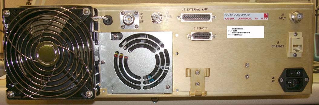
Click to zoom
Application Details
- Equipment Class
- TBC - Licensed Broadcast Station Transmitter
- Date of Grant
- Jan 06, 2008
- Application Purpose
- Original Equipment
- Date of Application
- Nov 25, 2007
- Equipment Note
- 50-Watt UHF Digital Transmitter
- Frequency Range
- 614.00000000 - 806.00000000
- Company
- UBS-Axcera
- Country
- United States
Documents & Files
Document Text
Text extracted from the exhibit documents filed with the FCC. Open a document above to read the original.
Users Manual
Preliminary Instruction Manual CU50ATD Innovator 50-Watt Transmitter AXCERA, LLC 103 FREEDOM DRIVE, P.O. Box 525 LAWRENCE, PA 15055-0525 USA (724) 873-8100 • FAX (724) 873-8105 www.axcera.com • [email protected] Innovator CU50ATD, 50 Watt Transmitter Table of Contents Instruction Manual, Rev. 0 August 14, 2007 CU50ATD INNOVATOR 50-WATT TRANSMITTER Introduction..................................................................................................1 Manual Overview.....................................................................................1 Assembly Designators..............................................................................1 Safety....................................................................................................1 Contact Information.................................................................................2 Return Material Procedure........................................................................2 Warranty Information...............................................................................3 Tray Description...........................................................................................10 8 VSB Demodulator Board......................................................................10 8 VSB Modulator Board..........................................................................10 Amplifier Assembly................................................................................11 2 Stage UHF Amplifier Board,...........................................................12 RF Module Pallet w/Philips Transistors...............................................12 Output Detector Board...........................................................................12 Tray Power Supplies...............................................................................13 Tray LCD Display and Front Panel LED Indicators.............................................13 Input and Output Connections.......................................................................14 Remote Connections.....................................................................................14 Front Panel Screens for the Transmitter..........................................................16 System Alignment........................................................................................19 Set Up of the Output Power of the Transmitter..........................................19 ALC Board Set-Up in the Transmitter.......................................................19 Linearity Correction Adjustment..............................................................20 Frequency Response Delay Equalization Adjustment..................................20 Appendix A Drawings List..............................................................................................A-1 Transmitter Specifications............................................................................B-1 Innovator CU50ATD, 50 Watt Transmitter Introduction Instruction Manual, Rev. 0 1 Manual Overview This manual describes the transmitter, along with the setup and alignment procedures for the transmitter. Assembly Designators Axcera has assigned assembly numbers, Ax designations such as A1, where x=1,2,3...etc, to all assemblies, modules, and boards in the system. These designations are referenced in the text of this manual and shown on the block diagram and interconnect drawings provided in the appendix. The cables that connect between the boards within a tray or assembly and that connect between the trays, racks and cabinets are labeled using Brady markers. Figure 1 is an example of a Brady marked cable. There may be as few as two or as many as four Markers on any one cable. These Brady markers are read starting furthest from the connector. If there are four Brady Markers, this marker is the transmitter number such as transmitter 1 or transmitter 2. The next or the furthest Brady Marker is the rack or cabinet number on an interconnect cable or the board number within a tray. The next number on an interconnect cable is the Tray location or number. The Brady marker closest to the connector is the jack or connector number on an interconnect cable or the jack or connector number on the board within a tray. Figure 1: Brady Marker Identification Drawing Safety The transmitter systems manufactured by Axcera are designed to be easy to use and repair while providing protection from electrical and mechanical hazards. Please review the following warnings and familiarize yourself with the operation and servicing procedures before working on the transmitter system. Read All safety Instructions – All of the safety instructions should be read and understood before operating this equipment. Retain Manuals – The manuals for the transmitter should be retained at the transmitter site for future reference. Axcera provides two manuals for this purpose; one manual can be left at the office while the other can be kept at the site. Heed all Notes, Warnings, and Cautions – All of the notes, warnings, and cautions listed in this safety section and throughout the manual must be followed. Follow Operating Instructions – All of the operating and use instructions for the transmitter should be followed. Cleaning – Unplug or otherwise disconnect all power from the equipment before cleaning. Do not use liquid or aerosol cleaners. Use a damp cloth for cleaning. Innovator CU50ATD, 50 Watt Transmitter Introduction Instruction Manual, Rev. 0 2 Ventilation – Openings in the cabinet and module front panels are provided for ventilation. To ensure the reliable operation of the driver/transmitter, and to protect the unit from overheating, these openings must not be blocked. Servicing – Do not attempt to service this product yourself until becoming familiar with the equipment. If in doubt, refer all servicing questions to qualified Axcera service personnel. Replacement Parts – When replacement parts are used, be sure that the part…
Text truncated - open the document above for the full version.
Cover Letter(s)
November 20, 2007 Federal Communications Commission 445 12th Street, SW Washington, DC 20554 Gentlemen: Axcera is submitting this FCC Equipment Authorization report for the CU50ATD, a 50-watt UHF digital television transmitter. We are applying for a low- power television, Equipment Authorization approval for this UHF transmitter. The FCC identifier selected for this product is OUSCU50ATD. The CU50ATD is a complete 50-watt UHF solid-state digital transmitter. It operates at a nominal output power of 50 watts average, while meeting or exceeding the FCC simple and stringent mask requirements. The transmitter may also be operated at 5 watts average with equivalent or improved performance. The CU50ATD will cover the frequencies of 470 MHz to 608 MHz & 614 MHz to 806 MHz. The enclosed application and test data report are intended to demonstrate compliance with FCC guidelines. Please contact me if you have any questions or if you need additional information. I can be reached by fax at (724) 873-8105 or phone at (724) 873-8100, extension 233. Sincerely, ______________________ David W. Brooking Principal Engineer
External Photos
Axcera-CU50ATD FCC Equipment Authorization Report External Photos November 2007 2-1 2. EXTERNAL PHOTOS 2.1 Front view, complete Axcera-CU50ATD Transmitter Axcera-CU50ATD FCC Equipment Authorization Report External Photos November 2007 2-2 2.2 Rear view, complete, Axcera-CU50ATD Transmitter
ID Label/Location Info
Axcera-CU50ATD FCC Type Acceptance Report ID Label/Location Info November 2007 1-1 1. ID LABEL/LOCATION INFO 1.1 Rear Panel FCC Label 1.2 Rear Panel Manufacturer’s Label Axcera-CU50ATD FCC Type Acceptance Report ID Label/Location Info November 2007 1-2 1.3 Rear view, Axcera-CU50ATD Transmitter with FCC Label and Manufacturer’s Label
Internal Photos
Axcera-CU50ATD FCC Equipment Authorization Report Internal Photos November 2007 6-1 6. INTERNAL PHOTOS 6.1 Top view, CU50ATD Transmitter
Operational Description
Axcera-CU50ATD Equipment Authorization Report Operational Description November 2007 8-1 8. OPERATIONAL DESCRIPTION - MODEL Axcera-CU50ATD 8.1 General Description The CU50ATD is a complete 50-watt UHF solid-state, digital television transmitter. It operates at a nominal output power of 50 watts average. 8.2 Technical Specifications Type of Emission .....................................................................6M00K1D Frequency Range........................470 MHz to 608 MHz and 614 to 806 MHz Output Power............................................................... 50 watts average 8.3 Performance Specifications Operating Frequency Range .........470 MHz to 608 MHz and 614 to 806 MHz RF output - Nominal: Power ............................................................... 50 watts average Impedance .................................................................... 50 ohms Connector ............................................................................ “N” Regulation of Output........................................................................ 3% Signal-to-Noise Ratio (SNR) ........................................... 27 dB or better Carrier Frequency Stability.......................................................... ±1 ppm Out of Band: Compliant with FCC Simple or Stringent Mask (Measured in 30 KHz RBW, relative to total average power) Data Interface: Input Rate.................................................... 19.39 Mbps, 6 MHz Channel Input Interface...............................................SMPTE 310M (ASI optional) Electrical Requirements Power Line Voltage .............................................117/230 volts, 50/60 Hz Power Consumption .............................................................. 1000 watts Environmental Maximum Altitude ..................................................................8,500 feet Operational Temperature Range ...........................................0°C to +50°C Axcera-CU50ATD Equipment Authorization Report Operational Description November 2007 8-2 Mechanical Dimensions: Width .............................................................. 19” (Rack mount) Height................................................................................. 3RU Weight ...........................................................................50 lbs 8.4. System Overview The CU50ATD is made up of the trays/assemblies listed in Table 8-1. Table 8-1. CU50ATD Major Trays and Assemblies MAJOR ASSEMBLY DESIGNATOR TRAY/ASSEMBLY NAME A1 Digital Transmitter Tray 8.4.1 Transmitter Tray The Transmitter accepts an RF On Channel signal (-79 to –8 dBm) and converts it to a DTV RF On Channel output signal at 50 Watts. The transmitter provides linear and nonlinear correction capability for the transmission path as well as internal test sources that are used during initial transmitter installation. 8.4.1.1 (A1) 8 VSB Demodulator Board (1308275) The RF input to the Transmitter is connected to the J1 BNC connector located on the rear panel of the tray. This RF signal is wired to (A1) the 8 VSB demodulator board (1308275), which generates a SMPTE-310 output at J13. The (A1) 8 VSB demodulator assembly receives an off air 8 VSB signal on any VHF or UHF channel and demodulates this to an MPEG-2 transport stream that is per the SMPTE-310M standard. The input to the assembly is at an “F” style connector on the shielded tuner and can be at a level of –78 dBm to –8 dBm. The tuner (TU1) down converts the RF channel to a 44 MHz IF signal. This IF signal is the input to the digital receiver chip U1. The digital receiver chip subsequently decodes the IF and delivers an MPEG-2 transport stream, on a parallel data bus, to a programmable logic array, U8. U8 clocks the asynchronous MPEG data from the receiver chip and outputs a synchronous data stream at a 19.39 MHz rate to buffer/driver U11. U11 subsequently drives the output at J13 to a lower level that is AC coupled out of the board and is cabled to J42 on the 8 VSB Modulator Board. 8.4.1.2 (A2) 8 VSB Modulator Board (1304883) The (A2) 8 VSB Modulator Board (1304883) accepts the SMPTE-310 MPEG data stream input at the SMA connector J42 and produces a 6 MHz wide IF output, at the IF Output Jack J38. The IF output is centered at 44 MHz using a pilot carrier of 46.69 MHz generated on the board. This SMPTE-310 MPEG data stream input is applied to a high-speed window comparator U21 that adjusts the level to a low voltage TTL signal to be used by the Altera FPGA, U3. The SMPTE-310 signal is input to the FPGA to recover the clock and the data. A portion of the clock and recovery circuit is performed by a high- speed comparator, U17, which functions as an external delay circuit. Axcera-CU50ATD Equipment Authorization Report Operational Description November 2007 8-3 The FPGA subsequently uses the SMPTE-310 clock and data as the input to the channel coder contained inside the FPGA. The channel coder is a series of DSP blocks defined by the ATSC standard for 8 VSB data transmission. These blocks include the data randomizer, Reed Solomon Encoder, data interleaver, trellis coder, and sync inserter. The channel coder portion, inside the FPGA, generates the 8 distinct levels in an 8 VSB transmitter. These levels are subsequently input to a linear equalizer that provides for frequency response correction in the transmission path. The linear equalizer is a 67-tap FIR filter that is loaded with tap values from the microcontroller, U1, located on this board. The output of the linear equalizer is then input to two pulse shaping filters, an in phase (I) and a quadrature (Q) filter that are also located inside the FPGA. The pulse shaping filters are FIR filters that have fixed tap values that are preset inside the FPGA. The output of the pulse shaping filters is then applied to a Pre-Distortion Linearizer chip, U4, which can be used to correct for nonlinearities in the data transmission path. The output of the Pre-Distortion chip is …
Text truncated - open the document above for the full version.
Parts List/Tune Up Info
Axcera-CU50ATD FCC Equipment Authorization Report Parts List/Tune-up Info November 2007 7-1 7. PARTS LIST/TUNE-UP INFO 7.1 Parts List The transmitter, can be subdivided as follows: 8 VSB Modulator Board Power Conditioning Board Digital Modulator Board Pre-Corrector Board ALC Board Output Detector Board Control Card Board Frequency Agile Upconverter Board Two Stage UHF Amplifier Board Amplifier Module Astec Switching Power Supply Densei-Lamda Switching Power Supply 7.2 Tune-Up Information This transmitter was aligned at the factory and should not require additional adjustments to achieve normal operation. This transmitter is of a tray design with multiple boards inside the tray. If a board fails, that board needs to be changed out with a replacement board. The failed board can then be sent back for repair. 7.2.1 Set-Up of the Output Power of the Transmitter Check that the Auto/Man switch S1 on the IF Pre-Corrector Board is in the Automatic ALC position. This is the normal operating position for the switch. The voltage at TP1 on the IF Pre-Corrector Board should be .8 VDC with 100% output power. Check that the Auto/Man switch S1 on the ALC Board is in the Automatic ALC position. Adjust R75 the ALC pot on the ALC Board as needed to attain 100% output power. Switch to Manual Gain (Manual ALC) and adjust the Manual Gain pot R62 for 100 % output power. Switch the ALC Board back to Automatic ALC. 7.2.2 ALC Board Set-Up In the Tray On (A5) the ALC Board (1308570), preset the Overdrive Threshold pot R38 full CW and set R62, Manual Adjust, and R75, ALC Adjust, full CCW. Apply an 8-VSB signal at -3 dBm average level to the J1 input jack to the tray. Switch S1 to Manual Gain, and increase the output power to 100%. Calibrate the transmitter output power using R23, Forward Calibration pot, on the Output Detector Board. Turn the output power down to 10% power. Remove the output RF connector from J2 on tray and calibrate the reflected power to 10%, using R7, the Reflected Calibration pot, on the Output Detector Board. Re-connect the RF output connector to the tray and increase the power, in Manual gain, to 110%. Adjust the Overdrive pot R38, CCW until the overdrive threshold just trips and the Overdrive Fault LED DS4 lights. Turn the pot Axcera-CU50ATD FCC Equipment Authorization Report Parts List/Tune-up Info November 2007 7-2 slightly CW so that power comes back up and DS4 goes out. Switch S1 to ALC. Turn the ALC Adjust pot R75 until the power is 100%. Switch S1 between ALC and Manual to verify smooth switching, with minimal change in power. Switch the tray Off and insert a 10 dB attenuator at the input. Switch the tray On and verify the input fault LED comes on and the RF power Mutes. Output power should drop by at least 20-30 dB. Switch the tray Off and remove the 10 dB attenuator. Replace the input connector and turn the tray back on. With the tray in ALC, use the ALC Adjust pot, R75, to decrease the power to 10%. Remove the RF output connector from the tray. Verify that the VSWR Cutback LED, DS6, comes on and the Reflected Power drops to approximately 6%. Reconnect the RF output connector and increase the power back up to 100%. This completes the set up of the ALC board. 6 MHz -35 dB -110 dB 3 MHz 6 MHz Figure 3: Typical Digital Spectrum 7.2.3 Linearity Correction Adjustment (Non-Linear Distortions) As shipped, the transmitter was preset to include amplitude and phase pre-distortion. The pre-distortion was adjusted to approximately compensate the corresponding non-linear distortions of the Power Amplifier. NOTE: On (A3) the IF pre-corrector board (1308796), check that the correction enable/disable jumper W4 on J8 is in the Enable position, between pins 2 & 3. Set up a spectrum analyzer with 30 kHz resolution bandwidth and 30 kHz video bandwidth to monitor the intermodulation products of the RF output signal of the Tray at J2. A typical digital spectrum is shown in Figure 3. There are three Corrector stages, two in phase and one quadrature, adjustments located on the IF Pre-Corrector Board. The adjustments are threshold settings that are adjusted as needed to correct for any amplitude or phase intermod problems. Adjust in phase linearity correction adjustment R67 threshold 1 cut in for the in phase amplitude distortion pre-correction that is needed. Next adjust the linearity correction adjustment R69 threshold 2 cut in also for the in phase amplitude distortion pre-correction that is Axcera-CU50ATD FCC Equipment Authorization Report Parts List/Tune-up Info November 2007 7-3 needed. Finally, adjust the quadrature linearity correction adjustment R89, threshold cut in, for the quadrature phase distortion pre-correction that is needed. The above pots are adjusted for the greatest separation between the digital signal and the intermod at the channel edges. 7.2.4 Frequency Response Delay Equalization Adjustment at 44 MHz The procedure for performing a frequency response delay equalization adjustment for the transmitter is described in the following steps. Check that the jumpers on J4, J5 & J6 are set for 44 MHz between Pins 2 & 3. The center frequency for the first stage is 46.5 MHz. Adjust R24, located on the IF Pre- Corrector Board, for the best depth of frequency response correction at 46.5 MHz. C14 may need to be adjusted to attain best depth at 46.5 MHz. The center frequency for the second stage is 41.5 MHz. Adjust R25 for the best depth of frequency response correction at 41.5 MHz. C15 may need to be adjusted to attain best depth at 41.5 MHz. The center frequency for the third stage is 44 MHz. Adjust R26 for the best depth of frequency response correction at 44 MHz. C16 may need to be adjusted to attain best depth at 44 MHz. After the three delay attenuation equalizers have been adjusted, fine tune, as needed, for the best frequency response across the channel. The transmitter is now set up and ready for normal operation.
Test Report
Axcera – CU50ATD Equipment Authorization Report Test Report November 2007 4-1 4. TEST REPORT 4.1 RF Power Measurements Figure 4-1 shows the test equipment setup for the RF power measurements. Figure 4-1. Test Equipment Setup for RF Power Measurements The output power of the CU50ATD was adjusted to obtain 50 watts average RF output as observed on the power meter. At this power level, the final Measured Power: +7 dBm Coupling Loss: -40.0 dB Power: +47.0 dBm Power = 50 Watts With the power level properly set to 50 watts average, all required tests were performed and recorded in the following sections. CU50ATD Transmitter Hewlett Packard Power Meter Bird Model 8892-300 50 Ohm Termination Connecticut Microwave Directional Coupler EFA 2067.3004.53 8VSB Demodulator HP Spectrum Anaylzer Device Under Test Bandpass Filter Directional Coupler Axcera – CU50ATD Equipment Authorization Report Test Report November 2007 4-2 4. 2 Modulation Characteristics The modulator tray incorporates a modulation technique known as 8-Level Vestigial Side-band (8-VSB), which uses a layered digital architecture and a single carrier frequency. A pilot tone is provided, to allow rapid acquisition of the signal by receivers. The 8-VSB system transmits a serial data bit stream at a rate of 19.4 Mbps in a 6 MHz television channel. This type of transmission is far less susceptible to propagation impairments such as multi-path, noise and interference as compared to analog transmissions. Figure 4-2. Typical Demodulation Test Setup CU50ATD Transmitter Directional Coupler 50 Ohm Termination HP 89441A Vector Signal Analyzer 20 dB Attenuator Laptop Computer Device Under Test EFA 2067.3004.53 8VSB Demodulator Bandpass Filter Directional Coupler Axcera – CU50ATD Equipment Authorization Report Test Report November 2007 4-3 4. 3 Error Vector Magnitude (EVM) and Signal to Noise Ratio (SNR) The Hewlett Packard Vector Signal Analyzer was used to measure that the un-equalized patterns are within the ATSC/FCC EVM limit of 4% and SNR limit of 27db. Figure 4-3. Constellation Diagram Axcera – CU50ATD Equipment Authorization Report Test Report November 2007 4-4 4. 4 Frequency Response Figure 4-4. Frequency Response Plot Axcera – CU50ATD Equipment Authorization Report Test Report November 2007 4-5 4. 5 Peak to Average Figure 4-5. Peak to Average Plot Axcera – CU50ATD Equipment Authorization Report Test Report November 2007 4-6 4. 6 Phase Noise Figure 4-6. Phase Noise Plot Axcera – CU50ATD Equipment Authorization Report Test Report November 2007 4-7 4.7 Occupied Bandwidth Using the test setup in Figure 4-2, with the transmitter operating at maximum power, a photograph of the transmitter occupied bandwidth spectrum was taken and is shown in Figure 4-7. Figure 4-7. Channel Occupied Bandwidth (Pre-Filter) Axcera – CU50ATD Equipment Authorization Report Test Report November 2007 4-8 4.8 Conducted Spurious Emissions The Hewlett Packard Spectrum Analyzer was used to measure harmonics before mask filter. Figure 4-8A. Out of Band Emissions Plot (Pre-Filter) The test data on the following pages demonstrates that the CU50ATD meets both the simple and stringent mask requirements. Axcera – CU50ATD Equipment Authorization Report Test Report November 2007 4-9 Simple Mask Test Data - Part 74.794 of the Rules states: (i) Simple mask. At the channel edges, emissions must be attenuated no less than 46 dB. More than 6 MHz from the channel edges, emissions must be attenuated no less than 71 dB. At any frequency between 0 and 6 MHz from the channel edges, emissions must be attenuated no less than the value determined by the following formula: A (dB) = 46 + (Df2 /1.44) (3) The attenuation values for the simple and stringent emission masks are based on a measurement bandwidth of 500 kHz. Other measurement bandwidths may be used and converted to the reference 500 kHz value by the following formula: A(dB) = Aalternate + 10 log (BWalternate / 500) where A(dB) is the measured or calculated attenuation value for the reference 500 kHz bandwidth, and Aalternate is the measured or calculated attenuation for a bandwidth BWalternate. Emissions include sidebands, spurious emissions and radio harmonics. Attenuation is to be measured at the output terminals of the transmitter (including any filters that may be employed). In the event of interference caused to any service by out-of-channel emissions, greater attenuation may be required. Mask data was measured for the filter with results plotted at 10 kHz steps. In the first 500 kHz adjacent to the channel edge, the out of band power must be 46 dB below the total channel power. To determine the out of band power, the amplifier IMD measured at the final amplifier output before the mask filter was added to the filter response and the power was summed over 500 kHz to give the total out of band power in that band. The total channel power can be found by multiplying the power in 10 kHz by the number of 10 kHz subsections in the occupied bandwidth. The ratio of the out of band to in band power is then calculated. Frequency Filter Response Amp IMD Total Power 590 -27.1 37 -64.1 3.89045E-07 590.01 -27.09 37 -64.09 3.89942E-07 590.02 -27.08 37 -64.08 3.90841E-07 590.03 -27.04 37 -64.04 3.94457E-07 590.04 -26.99 37 -63.99 3.99025E-07 590.05 -26.97 37 -63.97 4.00867E-07 590.06 -26.97 37 -63.97 4.00867E-07 590.07 -26.92 37 -63.92 4.05509E-07 590.08 -26.9 37 -63.9 4.0738E-07 590.09 -26.85 37 -63.85 4.12098E-07 590.1 -26.84 37 -63.84 4.13048E-07 590.11 -26.83 37 -63.83 4.14E-07 590.12 -26.8 37 -63.8 4.16869E-07 590.13 -26.75 37 -63.75 4.21697E-07 590.14 -26.73 37 -63.73 4.23643E-07 590.15 -26.69 37 -63.69 4.27563E-07 590.16 -26.69 37 -63.69 4.27563E-07 590.17 -26.66 37 -63.66 4.30527E-07 590.18 -26.61 37 -63.61 4.35512E-07 590.19 -26.6 37 -63.6 4.36516E-07 590.2 -26.57 37 -63.57 4.39542E-07 Axcera – CU50ATD Equipment Authorization Report Test Report November 2007 4-10 590.21 -26.54 37 -63.54 4.42588E-07 590.22 -26.49 37 -63.49 4.47713E-07 590.23 …
Text truncated - open the document above for the full version.
Test Report
Axcera-CU50ATD FCC Equipment Authorization Report Table of Contents November 2007 TABLE OF CONTENTS CHAPTER 1 ID LABEL/LOCATION INFO 1.1 Rear Panel FCC Label ........................................................................... 1-1 1.2 Rear Panel Manufacturer's Label ............................................................ 1-1 1.3 Front view, complete Axcera-CU50ATD Transmitter w/FCC Label ............... 1-2 1.4 Rear view, complete Axcera-CU50ATD Transmitter w/Manufacturer’s Label. 1-3 CHAPTER 2 EXTERNAL PHOTOS 2.1 Front view, complete Axcera-CU50ATD Transmitter ................................. 2-1 2.2 Rear view, complete Axcera-CU50ATD Transmitter .................................. 2-2 CHAPTER 3 Schematics CHAPTER 4 TEST REPORT 4.1 RF Power Measurements ...................................................................... 4-1 4.2 Modulation Characteristics .................................................................... 4-2 4.3 Error Vector Magnitude (EVM) and Signal to Noise Ratio (SNR)................ 4-3 4.4 Frequency Response ........................................................................... 4-4 4.5 Peak to Average .................................................................................. 4-5 4.6 Phase Noise ........................................................................................ 4-6 4.7 Occupied Bandwidth ............................................................................ 4-7 4.8 Conducted Spurious Emissions .............................................................. 4-8 4.9 Radiated Emissions.............................................................................4-42 4.10 Frequency Stability ...........................................................................4-44 4.11 Test Equipment ................................................................................4-46 CHAPTER 5 USER'S MANUAL CHAPTER 6 INTERNAL PHOTOS 6.1 Top view, Exciter ................................................................................ 6-1 CHAPTER 7 PARTS LIST/TUNE-UP INFO 7.1 Parts List ........................................................................................... 7-1 7.2 Tune-up Information ........................................................................... 7-1 7.2.1 Set-Up of the Out put Power of the Transmitter.............................. 7-1 7.2.2 ALC Board Set-Up in the Tray ...................................................... 7-1 7.2.3 Linearity Correction Adjustment (Non-Linear Distortions) ................ 7-2 7.2.4 Frequency Response Delay Equalization Adjustment at 44 MHz ........ 7-3 Axcera-CU50ATD FCC Equipment Authorization Report Table of Contents November 2007 CHAPTER 8 OPERATIONAL DESCRIPTION - MODEL Axcera-CU50ATD 8.1 General Description ............................................................................. 8-1 8.2 Technical Specifications.................................................................. 8-1 8.3 Performance Specifications ............................................................. 8-1 8.4 System Overview.......................................................................... 8-2 8.4.1 Transmitter Exciter Tray........................................................ 8-2 8.4.1.1 8 VSB Demodulator Board ................................................ 8-2 8.4.1.2 8 VSB Demodulator Board ................................................ 8-2 8.4.1.3 IF Pre-Corrector Board ..................................................... 8-3 8.4.1.4 Amplifier Assembly .......................................................... 8-4 8.4.1.5 2-Stage UHF Amplifier Board ............................................ 8-4 8.4.1.6 RF Module Pallet w/Phillips Transistors ............................... 8-4 8.4.1.7 Output Detector Board ..................................................... 8-5 8.4.5 AC Input ............................................................................. 8-5 8.4.6 Control & Status .................................................................. 8-5 8.4.7 Input and Output Connections ............................................... 8-6 8.4.8 Remote Connections................................…
Text truncated - open the document above for the full version.
Contact Information
Applicant
David Hewitt(Engineering Manager)
Technical Contact
AxceraDavid W. Brooking
[email protected]724-873-8100
103 Freedom Drive · Lawrence, Pennsylvania · United States
Non-Technical Contact
AxceraJames C. Mounts
[email protected]724-873-8100
Technical Specifications
| # | Rule Parts | Frequency Range | Power Output | Emission | Tolerance |
|---|---|---|---|---|---|
| 2 | 74 | 614 MHz - 806 MHz | 50 W | 6M00K1D | 1 ppm |
Other Applications from UBS-Axcera

OUSCU0TD-5-UBS
Mar 27, 2014200W UHF Digital Transmitter
Equipment Class
TBC - Licensed Broadcast Station Transmitter
OUSCL1TC-4
Sep 17, 2013400-Watt, 1.6 GHz DVB-H Transmitter
Equipment Class
TNB - Licensed Non-Broadcast Station Transmitter
OUSCLV2TD-4
Aug 22, 2013Low Band VHF Digital Broadcast Transmitter
Equipment Class
TBC - Licensed Broadcast Station Transmitter
OUSCHV4TD
Jun 14, 20123000-Watt VHF Digital Transmitter
Equipment Class
TBC - Licensed Broadcast Station Transmitter
OUSCU0TD-5
Dec 14, 2011200 Watt UHF Digital Transmitter
Equipment Class
TBC - Licensed Broadcast Station Transmitter