OUSLHV60ATD60-Watt VHF High Band Digital Transmitter
UBS-Axcera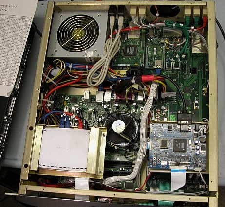
Click to zoom
Application Details
- Equipment Class
- TBC - Licensed Broadcast Station Transmitter
- Date of Grant
- Feb 10, 2008
- Application Purpose
- Original Equipment
- Date of Application
- Dec 30, 2007
- Equipment Note
- 60-Watt VHF High Band Digital Transmitter
- Frequency Range
- 174.00000000 - 216.00000000
- Company
- UBS-Axcera
- Country
- United States
Documents & Files
Document Text
Text extracted from the exhibit documents filed with the FCC. Open a document above to read the original.
Users Manual
INSTRUCTION MANUAL Axciter Digital Modulator/Upconverter System AXCERA, LLC 103 FREEDOM DRIVE P.O. BOX 525 LAWRENCE, PA 15055-0525 USA (724) 873-8100 • FAX (724) 873-8105 www.axcera.com • [email protected] Digital ATSC Exciter-Modulator System Table of Contents Axcera Axciter, Rev. 0 i March 22, 2007 CHAPTER 1: INTRODUCTION......................................................................................................................1 MANUAL OVERVIEW..........................................................................................................................................1 AXCITER OVERVIEW..........................................................................................................................................1 SAFETY...............................................................................................................................................................2 Read All Instructions.....................................................................................................................................2 Retain Manuals..............................................................................................................................................2 Heed Notes, Warnings, and Cautions............................................................................................................2 Follow Instructions........................................................................................................................................2 Cleaning........................................................................................................................................................2 Ventilation.....................................................................................................................................................2 Replacement Parts.........................................................................................................................................3 RETURN MATERIAL PROCEDURE........................................................................................................................3 WARRANTY FOR BROADCAST PRODUCTS...........................................................................................................4 Limited One-year Warranty...........................................................................................................................4 CHAPTER 2: INSTALLATION AND OPERATING INSTRUCTIONS......................................................5 INSTALLATION....................................................................................................................................................5 SETUP AND OPERATION PROCEDURES..............................................................................................................10 MODULATOR OPERATIONAL OVERVIEW..........................................................................................................10 USER INTERFACE..............................................................................................................................................11 Navigating the User Interface.....................................................................................................................11 User Interface Conventions.........................................................................................................................13 SCREEN DISPLAYS AND DETAILS......................................................................................................................15 Axciter Main Screen....................................................................................................................................15 Control and Status Screen...........................................................................................................................16 Signals Status Screen...................................................................................................................................17 Channel Offset Example..............................................................................................................................18 AXACT Equalizers.......................................................................................................................................19 Clock and Power Status Screen...................................................................................................................21 LED Status Screen.......................................................................................................................................22 History.........................................................................................................................................................24 DTVISION LINEAR - OPTIONAL.......................................................................................................................25 DTVision Linear Home/ Spectrum Screen...................................................................................................26 DTVision Constellation Screen....................................................................................................................27 DTVision Eye Screen...................................................................................................................................28 Linear Equalizer Graph...............................................................................................................................29 Linear Quad Display Screen.......................................................................................................................30 DTVISION NON-LINEAR - OPTIONAL...............................................................................................................31 DTVision Non-Linear Home/Spectrum Screen.........................................................................................…
Text truncated - open the document above for the full version.
External Photos
Axcera-LHV60ATD FCC Equipment Authorization Report External Photos December 2007 2-1 2. EXTERNAL PHOTOS 2.1 Front view, complete LHV60ATD Transmitter Axcera-LHV60ATD FCC Equipment Authorization Report External Photos December 2007 2-2 2.2 Rear view, complete Axcera-LHV60ATD Transmitter Axcera-LHV60ATD FCC Equipment Authorization Report External Photos December 2007 2-3 2.3 Rear View, Bandpass Filter Axcera-LHV60ATD FCC Equipment Authorization Report External Photos December 2007 2-4 2.4 Front View, External Axciter Digital Modulator 2.5 Rear View, External Axciter Digital Modulator 2.6 Top View, External Axciter Digital Modulator
ID Label/Location Info
Axcera-LHV60ATD FCC Equipment Authorization Report ID Label/Location Info December 2007 1-1 1. ID LABEL/LOCATION INFO 1.1 Rear Panel FCC Label 1.2 Rear Panel Manufacturer’s Label Axcera-LHV60ATD FCC Equipment Authorization Report ID Label/Location Info December 2007 1-2 1.3 Rear view, complete Axcera-LHV60ATD Transmitter with FCC Label and Manufacturer’s Label
Internal Photos
Axcera-LHV60ATD FCC Equipment Authorization Report Internal Photos December 2007 6-1 6. INTERNAL PHOTOS 6.1 Front view – Chassis Assembly Axcera-LHV60ATD FCC Equipment Authorization Report Internal Photos December 2007 6-2 6.2 Side view - Axciter Upconverter Assembly - Used with Axciter Modulator (Exciter) 6.3 Side view – Axciter Downconverter Assembly - Used with Axciter Modulator (Exciter) Axcera-LHV60ATD FCC Equipment Authorization Report Internal Photos December 2007 6-3 6.4 Side view - Control / Power Supply Assembly 6.5 Side view - Power Amplifier Assembly Axcera-LHV60ATD FCC Equipment Authorization Report Internal Photos December 2007 6-4 6.6 Top view – External Axciter Digital Modulator
Operational Description
Axcera-LHV60ATD FCC Equipment Authorization Report Operational Description December 2007 8-1 8. OPERATIONAL DESCRIPTION - MODEL Axcera-LHV60ATD 8.1 General Description The LHV60ATD is a complete 60-watt High-band VHF solid-state, digital transmitter. It operates at a nominal output power of 60 watts average. 8.2 Technical Specifications Type of Emission .....................................................................6M00K1D Frequency Range....................... 174 MHz to 216 MHz (any 6-MHz channel) Output Power........................................................... 60 watts average 8.3 Performance Specifications Operating Frequency Range ...................................... 174 MHz to 216 MHz RF output - Nominal: Power ............................................................... 60 watts average Impedance .................................................................... 50 ohms Connector ............................................................................ “N” Regulation of Output........................................................................ 3% Signal-to-Noise Ratio (SNR) .............................................. 33 dB typical Carrier Frequency Stability.......................................................±1000 Hz Out of Band: Compliant with FCC Mask (Measured in 30 KHz RBW, relative to total average power Channel Edge ± 500 KHz................................................ -47 dB or better 6 MHz Channel Edge .....................................................-110 dB or better Data Interface: Input Rate.................................................... 19.39 Mbps, 6 MHz Channel Input Interface..........................SMPTE 310M, Serial Differential ECL & TTL Electrical Requirements Power Line Voltage .............................................110-260 volts, 50/60 Hz Power Consumption ................................................................ 725 watts Environmental Maximum Altitude ..................................................................8,500 feet Operational Temperature Range ...........................................0°C to +50°C Axcera-LHV60ATD FCC Equipment Authorization Report Operational Description December 2007 8-2 Mechanical Dimensions: Width ..........................................................................22 inches Depth ..........................................................................34 inches Height..........................................................................55 inches Weight ............................................................................ 250 lbs 8.4. System Overview The LHV60ATD is made up of the trays listed in Table 8-1. Table 8-1. LHV60ATD Major Trays and Assemblies MAJOR ASSEMBLY DESIGNATOR TRAY/ASSEMBLY NAME A1 Axciter Modulator Tray A2 VHF HB Exciter Assembly 8.4.1 Exciter Tray 8.4.1.1 Axciter – Enternal Digital Modulator The Axciter modulator is an ATSC compliant 8 VSB modulator that is used externally with the Innovator LX Driver chassis assembly. The Axciter modulator also accepts a SMPTE-310 MPEG data stream input and outputs a 6 MHz wide IF output centered at 44 MHz. All of the functions of the Axciter modulator are controlled from the front panel pushbuttons. 8.4.1.2 Axciter Upconverter Module The 44 MHz IF input, -6 dBm in level, to the upconverter module assembly is applied through the backplane board from the modulated IF input jack located on the rear of the HX or LX exciter/driver chassis assembly. The 44 MHz IF input to the upconverter/downconverter tray connects through J5, the IF input jack located on the rear panel. The signal connects to the First Conversion board and is converted to a second IF of 1044 MHz by an image rejection mixer located on the First Conversion board. A filter selects the appropriate conversion product, which is then amplified to a level of approximately –8 dBm. The 1 GHz LO frequency is generated externally by the Axciter modulator and is applied to a high pass and low pass filter designed to eliminate any other interfering signals that might be coupled into the 1 GHz LO. The LO is applied to an ALC circuit that maintains the LO level to each mixer of +13 dBm over a wide range of 1 GHz LO input levels. The LO sample is also sent to the Downconverter board inside the tray or to the external Downconverter module for its use. This second IF signal is then applied to a second mixer mounted on the Final Conversion board that converts it back to a broadcast channel (2-69) by an LO that operates in 1.0 MHz steps between 1.1-1.9 GHz depending on the channel selected. The LO frequency equals the Channel center frequency plus 1044 MHz. (As an example CH: 14: Center Frequency is 473.00 MHz therefore LO2 is 473 + 1044, which equals 1517.00 MHz.) Axcera-LHV60ATD FCC Equipment Authorization Report Operational Description December 2007 8-3 The output of the mixer is applied to a 900 MHz Low pass filter to remove unwanted conversion products. The resulting signal is amplified and wired to a Pin diode attenuator and then connected to the output of the Upconverter/Downconverter Tray or the output of the Upconverter Module. This pin diode attenuator adjusts the gain of the tray or module and is controlled by an Automatic Gain Control circuit, which maintains a constant power out of the upconverter, and also the transmitter, that connects to the power amplifier module. Processor board detects an Input Signal fault it automatically Mutes the transmitter. The system controller does not Mute on an IF Processor Input fault. The Axciter upconverter module has no need for periodic alignment. 8.4.1.3 Axciter Downconverter Module A sample of the transmitter’s RF output is applied to the downconverter board, mounted on the downconverter module, at a nominal input level of –6 dBm. The signal is attenuated by a 10 dB pad, and then converted to an IF of 1044 MHz by mixer U1. A sample of the upconversion LO from the L-Band PLL Board mounted in the upconv…
Text truncated - open the document above for the full version.
Parts List/Tune Up Info
Axcera-LHV60ATD FCC Type Acceptance Report Parts List/Tune-up Info December 2007 7-1 7. PARTS LIST/TUNE-UP INFO 7.1 Parts List The transmitter, can be subdivided as follows: External Axciter Digital Modulator Tray Exciter Tray, consisting of: Axciter Upconverter Axciter Downconverter Control & Monitoring / Power Supply Module Power Amplifier Module 7.2 Tune-up Information The LHV60ATD transmitter was aligned at the factory and should not require additional alignments to achieve normal operation. 7.2.1 Exciter Assembly This transmitter takes the IF from the digital modulator and converts the signal to the desired High-Band VHF On Channel RF Output at the systems output power level. Switch On the main AC for the system and the individual circuit breakers on each assembly. Check that AC is present to the system. Check that the RF output of the post-filter coupler assembly is terminated into a dummy load of at least the rated output of the system or connected to the antenna for your system. While performing the alignment, refer to the Test Data Sheet for the transmitter and compare the final readings from the factory with the readings on each of the modules. The readings should be very similar. If a reading is way off, the problem is likely to be in that module. This transmitter operates using a SMPTE 310 input that connects to J27, the MPEG Input Jack, located on the rear of the Axciter Modulator Tray. Check that the MPEG input is present. If used, check that the 10 MHz input from the GPS is connected to J9 on the Axciter Modulator. The check of and the setup of the drive level and output power of the transmitter are completed using the LCD Display on the control/power supply module. In the Transmitter Set-Up menu and the Power Control Screen, set the output power to 100% or the drive level needed to attain the desired output power of the transmitter. The transmitter must be in the Manual Gain position when readjusting the Forward Power. The adjustment of the linearity and phase pre-distortion to compensate for any nonlinear response of the Power Amplifiers are controlled within the Axciter Modulator Tray. Axcera-LHV60ATD FCC Type Acceptance Report Parts List/Tune-up Info December 2007 7-2 7.2.1.1 Upconverter Downconverter Adjustment On the Axciter Modulator, activate the Upconverter Main screen by selecting Upconverter, using the button next to Upconverter on the right side of the Axciter Main Screen. Activate the Downconverter Output Gain by pushing 2 on the key board entry pad. Monitor the DTVision Linear Display by pushing the button next to the DTVision Linear display on the right side of the Axciter Main Screen. At the bottom of the DTVision linear screen, locate the reading next to RMS. If this reading is between –10 dBm and 0 dBm no adjustment is needed. If it is not, adjust the “Downconverter Gain”, then view the RMS value until it is within the –10 dBm to 0 dBm range. 7.2.1.2 Forward Power Calibration Check that the transmitter is at 100% output power, as shown on the LCD display on the Driver/Amplifier in the Set Up menus. Measure with a VOM, TP31-14, Red, and TP31-12, Black, on the terminal block TP31, located on the rear chassis of the Driver/Amplifier Chassis Assembly. Adjust R9, Forward Calibration Adjustment, on the Dual Peak Detector Board (1159965) for a reading of .8VDC on the VOM. Locate the Forward Power Adjust screen on the Driver/Amplifier LCD display in the Set Up menus and adjust the up or down arrow as needed to achieve 100 % output power. This completes the forward power set up. 7.2.1.3 Reflected Power Calibration Switch the transmitter to Standby. Remove the connector that is on Jack J2, on the Dual Peak Detector Board (1159965), and replace with the connector now on J1, also inserting a 10 dB pad in series. Switch the transmitter to operate. Then adjust R10, Reflected Calibration Adjustment, on the dual peak detector board (1159965) for a .32VDC reading, at TB31-13 and TB31-12 return, on the terminal block TB31 mounted on the rear of exciter/driver chassis assembly. Switch the transmitter to Standby. Move the connector back to J1 while removing the 10 dB pad. Replace the original connector onto J2. Axcera-LHV60ATD FCC Type Acceptance Report Parts List/Tune-up Info December 2007 7-3 7.2.2 Axciter Digital Modulator The Digital Modulator has adjustments for modulation levels, and other related parameters. Switch the transmitter to Standby. The ALC is muted when the transmitter is in Standby. To monitor the ALC, preset R3, manual gain-adjust, on the front panel of the Upconverter module, fully CCW. Move switch SW1, Auto/Man AGC, on the front panel of the Upconverter module, to the Manual position. Place the transmitter in Operate. Adjust the ALC GAIN pot on the front panel of the IF Processor to obtain +0.8 VDC on the LCD Display on the Controller/Power Supply in the ALC screen. Move the MAN/AUTO ALC switch back to Auto, which is the normal operating position. To adjust the AGC Cutback setting, raise the output power of the transmitter to 110%. Adjust R2, AGC Cutback, located on the front panel, CCW until the LED DS1, AGC Cutback, just starts to flash. Return the output power of the transmitter to 100%. 7.2.3 Bandpass Filter Assembly The Bandpass Filter Assembly is tuned to reject unwanted distortion products generated when the signals are diplexed and also during the amplification process. The Bandpass Filter is factory tuned to the proper bandwidth and should not need tuned. If you think tuning is needed consult Axcera Field Support Department before beginning the adjustment. The Transmitter is ready for normal operation. This completes the detailed alignment procedures for the transmitter.
Schematics
PA25-VHF-H-34 25W VHF Band III TV Linear Pallet Amplifier web http://www.drft.com • email : [email protected] • 1.775.DELTA RF • FAX 1.775.DELTA FX Delta RF Technology, Inc. • 801 East Glendale Ave • Sparks • NV • 89431 • U S A The specifications contained herein are subject to change without notice. Delta RF Technology, Inc. assumes no liability for the use of this information. © Delta RF Technology, Inc., 2004. Rev 1.b 03/04 High Power RF Amplifiers and Accessories The PA25-VHF-H-34 is a versatile output or driver pallet amplifier. Offering a minimum of 34dB gain, this two stage amplifier can be used as a driver or output stage depending on the application. With no circuit changes required, the PA25-VHF-H-34 can be configured as a Class A driver or Class AB output stage offering excellent flexibility. All gold-metallized MOSFETS are used in construction. • No RF assembly or circuit tuning! • 25 Watts of Linear Output Power Minimum! • 34dB typical gain at Channel 13! • Combined Video and Aural at full rated power! • Modular Construction for ease of Integration! retemaraPniMpyTxaMstinU PEP,tuoPlatnemadnuF cBd03-3DMI,zHM612-512,enot-2 05sttaW cnySkP,tuOrewoPraeniL5204sttaW tupnIrewoP80131mBd+ niaGrewoP43Bd AN-CSTN,deRdleiFlluF,DMI tuptuoderisednahtrettebBd01langistupniroF 45-85-cBd tnerruCniarD3A RWSVtupnI1:1.11:4.1 noitairaVesahPnoitresnI )tinuottinu( 5±° noitairaVniaGrewoP )tinuottinu( 1±Bd cinomraHdnoceS2F51-cBd cinomraHdrihT3F52-cBd pmeTgnitarepOetalpesaB006+C° snoisnemiDlacisyhP mc3xmc31xmc5/"0.1x"0.5x"0.2 Specifications: Vsup=+28V dc , I dq =2.77A, 170-230MHz retemaraPeulaVstinU egatloVgnitarepOmumixaM0.23+CDV egatloVgnitarepOelbatS0.23+ot0.62+CDV 1Q,tnerruCsaiBmumixaM .A020.0ottesyrotcaF 52.0A 4Q,tnerruCsaiBmumixaM .A57.2ottesyrotcaF 0.3A tnerruCniarDlatoTmumixaM5A lavivruShctamsiMdaoL dnaC04tadlehetalpesabehthtiwselgnaesahpllatA mumixamsdnoces2,A5otdetimiltnerrucdI 1:3 erutarepmeTegarotS501+ot04-C° gnitarepOmumixaM erutarepmeTetalpesaB 06+C° Absolute Maximum Ratings: Features Include: •Temperature Compensated Bias •Temperature Controller- Analog Temp Output •High Temp alarm with automatic PA disable •High Temp alarm output •Amplifier Disable •Current Sense, Each Transistor •Connectorized Power and I/O All values listed are without pre-correction. PA25-VHF-H-34 25W VHF Band III TV Linear Pallet Amplifier web http://www.drft.com • email : [email protected] • 1.775.DELTA RF • FAX 1.775.DELTA FX High Power RF Amplifiers and Accessories Pin Vs. Pout 0 2 4 6 8 10 12 14 3537394143 45 Output Power CW, +dBm Input Power CW, +dBm IMD vs. Pout -59.0 -58.0 -57.0 -56.0 -55.0 -54.0 -53.0 37383940414243 Power Out Pk Sync- +dBm IMD, FFR NTSC This amplifier has been designed for two purposes - as an output stage and as an ultra-linear driver. Driver - the amplifier is shipped from the factory biased best case for driver use from 2 - 20W, depending on needed output power (please see curves above). Frequency specific improvements may be made by adjusting the bias on Q1 (refer to page 4). Do not exceed rated bias current for Q1. Output Stage - for improved harmonic performance and efficiency, reset bias for Q1 to 0.250A, and reset bias to Q4 to 0.500A. Minor adjustments may need to be performed on Q1 / Q4 for optimum IMD performance. Do not exceed rated bias current for Q1. PA25-VHF-H-34 25W VHF Band III TV Linear Pallet Amplifier web http://www.drft.com • email : [email protected] • 1.775.DELTA RF • FAX 1.775.DELTA FX High Power RF Amplifiers and Accessories Tips for Mechanical Mounting: 1All holes are clear for #6 Screw. Stainless Steel mounting hardware is recommended, grade 18-8 or better. A lock washer of same material should also be used. 2Ensure mounting surface is flat to better than 0.003” / “ 3Use a thin layer of thermal compound on the backside of the PA - no more than 0.001” - 0.002” thickness! 4Torque all screws to 10-12 in-lbs Considerations for Mechanical Mounting: •Considerations for proper thermal design include •Total power dissipated = Total DC Power Consumed x (1-Efficiency) •Ambient Airflow •Thermal Resistance of Heat Sink For this PA, typical DC efficiency is 30%. At 25W Pk power output, 15W Average, +28.0V DC operation, 84 total watts are consumed, which leaves 70W dissipated power. If we assume an input air temperature of +25°C, and a maximum desired baseplate temperature of 55°C, this leaves a temperature differential between baseplate and ambient air of 30°C. The desired thermal resistance for heatsink mounting surface to air is therefore 30°C/74W = 0.4°C/W. Since the baseplate is aluminum, it is important to find a heat sink that it sized at least as big as the outline of the PA which can give this thermal resistance. For example, a 100mm x 54mm heat sink with serrated fins, 70mm in length, (20 fins across 127mm dimension) with an air velocity of 4 m / s exceeds this value. RF IN RF OUT PA25-VHF-H-34 25W VHF Band III TV Linear Pallet Amplifier web http://www.drft.com • email : [email protected] • 1.775.DELTA RF • FAX 1.775.DELTA FX High Power RF Amplifiers and Accessories O/I :redaehCDI/PIDhctip"001.0dradnatS DSCH,DSDIepytCETMAS 1010-60198epytM3 1-893201,1-393201PMA 603-20617GREB -ro- rotcennocO/IniniPotyltceridredloS 1-1J TUO_MRALAC07sdeecxeetalpesabnehwiHLTT 2-1J NI_MRALA tanwodtuhscitamotuarof1-1JotrepmuJ C06taselbane-eryllacitamotua,C07 3-1J DNUORG 4-1J PUS_SAIB yllanretnipusV.reifilpmasihtrofdesutoN .erehdetcennoc 5-1J PMETerutarepmeTetalpesaB 6-1J ELBASIDreifilpmaelbasiDotiHLTT rewoP :rotcennoCorciMmm0.3 0001-52034XELOM 7000-03034,1000-03034niPXELOM 0-716497-1PMA 606497,016497niPPMA -ro- ottnecajdadapotyltceridredloS rotcennoc 01,1-2J TNERRUC4Q,1QrotsisnarT,esneStnerruC 9,8,3,2-2J DNUORGdnuorGmetsyS 7,6,5,4-2J pusVCDV23+ot82+ Connections: Connect amplifier to +Vsup and Ground using either 3.0mm modular 10-position plug (J2) or soldering directly to pad adjacent to connector. If using Single connection, 14 gauge wire is recommended, 12 gauge ground wire. 20 gauge wire is recommende…
Text truncated - open the document above for the full version.
Schematics
P200-VHF-H-16 200W VHF Band III TV Linear Pallet Amplifier web http://www.drft.com • email : [email protected] • 1.775.DELTA RF • FAX 1.775.DELTA FX Delta RF Technology, Inc. • 801 East Glendale Ave • Sparks • NV • 89431 • U S A The specifications contained herein are subject to change without notice. Delta RF Technology, Inc. assumes no liability for the use of this information. © Delta RF Technology, Inc., 2004. Rev 1.b 04/04 High Power RF Amplifiers and Accessories The P200-VHF-H-16 is an integrated TV linear amplifier designed for the television integrator. Providing a minimum of 175W Pk sync linear power, the P200-VHF-H-16 is the perfect amplifier for any low band VHF transmitter. This cost effective build- ing block makes a great IPA or can be combined in multiple arrays for high power PAs. • No RF assembly or circuit tuning! • 200 Watts of Output Power! • 16dB typical gain at Channel 13! • Combined Video and Aural at full rated power! • Modular Construction for ease of Integration! retemaraPniMpyTxaMstinU Bd1P,tuOrewoP35mBd+ cnySkP,tuOrewoPraeniL cBd45-DMI,AN-CSTN,deRdleiFlluF 571sttaW cnySkP,tupnIrewoP58sttaW niaGrewoP5161Bd tnerruCniarD cnySkPW002=tuoP 0111A RWSVtupnI1:2.11:5.1 noitairaVesahPnoitresnI )tinuottinu( 5±° noitairaVniaGrewoP )tinuottinu( 1±Bd cinomraHdnoceS2F53-cBd cinomraHdnoceS3F51-cBd pmeTgnitarepOetalpesaB007+C° snoisnemiDlacisyhP mc4xmc01xmc5/"5.1x"0.4x"0.2 Specifications: Vsup=+28V dc , I dq =0.8A, 170-230MHz retemaraPeulaVstinU egatloVgnitarepOmumixaM0.43+CDV egatloVgnitarepOelbatS0.23+ot0.62+CDV tnerruCsaiBmumixaM .A8.0ottesyrotcaF 0.3A tnerruCniarDmumixaM mumixamA02rofdetarrotcennoc001J-etoN 41A rewoPtupnImumixaM04mBd+ lavivruShctamsiMdaoL dnaC04tadlehetalpesabehthtiwselgnaesahpllatA mumixamsdnoces2,A21otdetimiltnerrucdI 1:5 erutarepmeTegarotS501+ot04-C° gnitarepOmumixaM erutarepmeTetalpesaB 07+C° Absolute Maximum Ratings: Features Include: •Temperature Compensated Bias •Amplifier Disable •Current Sense •Connectorized Power and I/O P200-VHF-H-16 200W VHF Band III TV Linear Pallet Amplifier web http://www.drft.com • email : [email protected] • 1.775.DELTA RF • FAX 1.775.DELTA FX High Power RF Amplifiers and Accessories Pin vs. Pout 25 30 35 40 45 4547495153 Pout - CW +dBm Pin - CW +dBm 175 MHz 200 MHz 225 MHz Gain Compression -0.5 0 0.5 1 1.5 2 2.5 3 3.5 4 495051525354 Pout - CW +dBm Gain Compression dB 175 MHz 200 MHz 225 MHz Efficiency 10% 15% 20% 25% 30% 35% 40% 45% 50% 55% 454749515355 Pout - Video SLB +dBm Pk Sync Efficiency Ch 7Ch 9 Ch 11,13 Shaded Area denotes recommended operating power level P200-VHF-H-16 200W VHF Band III TV Linear Pallet Amplifier web http://www.drft.com • email : [email protected] • 1.775.DELTA RF • FAX 1.775.DELTA FX High Power RF Amplifiers and Accessories Tips for Mechanical Mounting: 1All holes are clear for #6 Screw. Stainless Steel mounting hardware is recommended, grade 18-8 or better. A lock washer of same material should also be used. 2Ensure mounting surface is flat to better than 0.003” / “ 3Use a thin layer of thermal compound on the backside of the PA - no more than 0.001” - 0.002” thickness! 4Torque all screws to 10-12 in-lbs Considerations for Mechanical Mounting: •Considerations for proper thermal design include •Total power dissipated = Total DC Power Consumed x (1-Efficiency) •Ambient Airflow •Thermal Resistance of Heat Sink P200-VHF-H-16 200W VHF Band III TV Linear Pallet Amplifier web http://www.drft.com • email : [email protected] • 1.775.DELTA RF • FAX 1.775.DELTA FX High Power RF Amplifiers and Accessories rewoP :rotcennoCorciMmm0.3 0001-52034XELOM 7000-03034,1000-03034niPXELOM 0-716497-1PMA 606497,016497niPPMA -ro- ottnecajdadapotyltceridredloS rotcennoc 1-101J TNERRUCesneStnerruC 9,8,3,2-101J DNUORGdnuorGmetsyS 5,4-101J pusVCDV23+ot82+ 01,7,6-101J C/NnoitcennoCoN Connections: Connect amplifier to +Vsup and Ground using either 3.0mm modular 10-position plug (J101) or soldering directly to pad adjacent to connector. If using Single connection, 14 gauge wire is recommended, 14 gauge ground wire. 20 gauge wire is recommended for use in modular connector, and all power connections must be used! In all cases, use of teflon insulated wire is highly recommended. Amplifier Startup +Vsup should be applied to amplifier with no drive applied. The system must allow drain voltage to reach +26V minimum before applying drive or damage can result to the amplifier and void warranty. This typically takes between 2 - 10 seconds and should be verified by the system integrator. The amplifier may be disabled by applying ground to TP1, …
Text truncated - open the document above for the full version.
Contact Information
Applicant
David Hewitt(Engineering Manager)
Technical Contact
AxceraLance R. Trussa
[email protected]724-873-8100
103 Freedom Drive · Lawrence, Pennsylvania · United States
Non-Technical Contact
AxceraJames C. Mounts
[email protected]724-873--8100
Technical Specifications
| # | Rule Parts | Frequency Range | Power Output | Emission | Tolerance |
|---|---|---|---|---|---|
| 1 | 74 | 174 MHz - 216 MHz | 60 W | 6M00K1D | 1000.0000000000 Hz |
Other Applications from UBS-Axcera

OUSCU0TD-5-UBS
Mar 27, 2014200W UHF Digital Transmitter
Equipment Class
TBC - Licensed Broadcast Station Transmitter
OUSCL1TC-4
Sep 17, 2013400-Watt, 1.6 GHz DVB-H Transmitter
Equipment Class
TNB - Licensed Non-Broadcast Station Transmitter
OUSCLV2TD-4
Aug 22, 2013Low Band VHF Digital Broadcast Transmitter
Equipment Class
TBC - Licensed Broadcast Station Transmitter
OUSCHV4TD
Jun 14, 20123000-Watt VHF Digital Transmitter
Equipment Class
TBC - Licensed Broadcast Station Transmitter
OUSCU0TD-5
Dec 14, 2011200 Watt UHF Digital Transmitter
Equipment Class
TBC - Licensed Broadcast Station Transmitter