OUSLLV20AL20-Watt VHF Low Band Translator
UBS-Axcera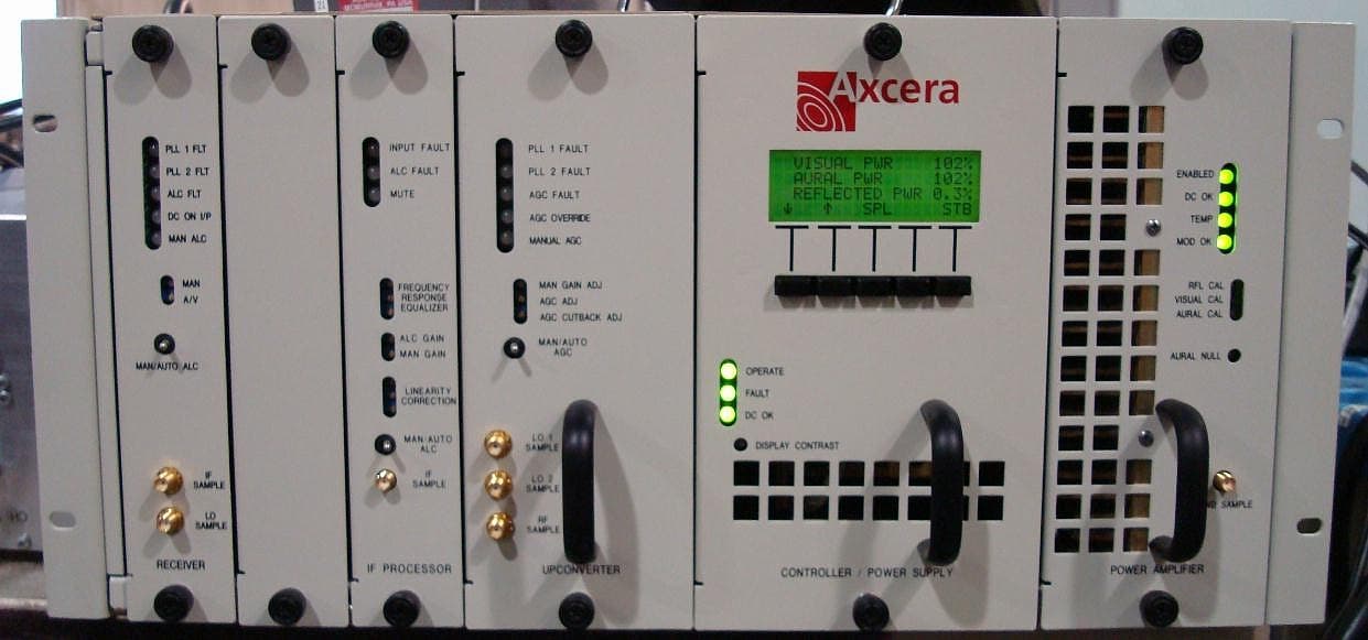
Click to zoom
Application Details
- Equipment Class
- TBC - Licensed Broadcast Station Transmitter
- Date of Grant
- Oct 25, 2007
- Application Purpose
- Original Equipment
- Date of Application
- Sep 06, 2007
- Equipment Note
- 20-Watt VHF Low Band Translator
- Frequency Range
- 76.00000000 - 88.00000000
- Company
- UBS-Axcera
- Country
- United States
Documents & Files
Document Text
Text extracted from the exhibit documents filed with the FCC. Open a document above to read the original.
Users Manual
INSTRUCTION MANUAL Innovator LX Series Analog VHF Translator AXCERA, LLC 103 FREEDOM DRIVE P.O. BOX 525 LAWRENCE, PA 15055-0525 USA (724) 873-8100 • FAX (724) 873-8105 www.axcera.com • [email protected] LX Series VHF Translator Table of Contents LX Series, Rev. 0 iv TABLE OF CONTENTS CHAPTER 1 INTRODUCTION SECTION PAGE 1.1 Manual Overview...................................................................................1-1 1.2 Assembly Designators............................................................................1-1 1.3 Safety..................................................................................................1-2 1.4 Contact Information...............................................................................1-2 1.5 Return Material Procedure......................................................................1-2 1.6 Limited One Year Warranty for Axcera Products........................................1-3 CHAPTER 2 SYSTEM DESCRIPTION, MAINTENANCE & REMOTE CONTROL CONNECTIONS 2.0 System Overview..................................................................................2-1 2.2 Exciter/Amplifier Chassis Assembly.........................................................2-2 2.2.1 Receiver Module...........................................................................2-2 2.2.2 IF Processor Module.....................................................................2-2 2.2.3 VHF/UHF Upconverter Module........................................................2-5 2.2.4 Control & Monitoring/Power Supply Module.....................................2-6 2.2.5 Exciter Power Amplifier Module, VHF HB.........................................2-8 2.3 RF Output Assemblies..........................................................................2-10 2.4 Control and Status...............................................................................2-10 2.5 System Operation................................................................................2-10 2.5.1 Principles of Operation................................................................2-10 2.6 Maintenance.......................................................................................2-11 2.7 Customer Remote Connections.............................................................2-12 CHAPTER 3 SITE CONSIDERATIONS, INSTALLATION AND SETUP PROCEDURES 3.1 Site Considerations................................................................................3-1 3.2 Unpacking the Cabinet, Chassis w/Modules and DTV mask filter.................3-4 3.3 Installing the Chassis w/Modules and filters..............................................3-4 3.4 AC Input...............................................................................................3-6 3.5 Setup and Operation..............................................................................3-6 3.5.1 Input Connections........................................................................3-6 3.5.2 Initial Turn On.............................................................................3-7 3.5.2.2 Receiver Module LEDs on Front Panel....................................3-8 3.5.2.3 IF Processor Module LEDs on Front Panel...............................3-8 3.5.2.4 VHF/UHF Upconverter Module LEDs on Front Panel.................3-8 3.5.2.5 Controller Module LEDs on Front Panel..................................3-8 3.5.2.6 Power Amplifier Module LEDs on Front Panel..........................3-8 3.5.3 Front Panel Screens for the Exciter/Amplifier Chassis Assembly.........3-9 3.5.5 Operation Procedure...................................................................3-18 LX Series VHF Translator Table of Contents LX Series, Rev. 0 v TABLE OF CONTENTS - (Continued) CHAPTER 4 CIRCUIT DESCRIPTIONS 4.2 Receiver Module (not used in the digital translator system)........................4-1 4.2.1 IF ALC Board...............................................................................4-1 4.2.2 VHF Mixer/PLL Board....................................................................4-2 4.2.3 VHF High Band Preamplifier Board.................................................4-2 4.3 IF Processor Module...............................................................................4-2 4.3.1 IF Processor Board.......................................................................4-3 4.3.1.1 Modulator Selected..............................................................4-3 4.3.1.2 External Modulated IF Selected.............................................4-3 4.3.1.3 Main IF Signal Path (Part 1 of 3)...........................................4-3 4.3.1.4 Input Level Detector Circuit..................................................4-3 4.3.1.5 Pin-Diode Attenuator Circuit.................................................4-5 4.3.1.6 Main IF Signal Path (Part 2 of 3)...........................................4-5 4.3.1.7 Amplitude and Phase Pre-Correction Circuits..........................4-6 4.3.1.8 Main IF Signal Path (Part 3 of 3)...........................................4-7 4.3.1.9 ALC Circuit.........................................................................4-7 4.3.1.10 Fault Command.................................................................4-8 4.3.1.11 ±12 VDC needed to operate Board......................................4-8 4.4 VHF/UHF Upconverter Module.................................................................4-8 4.4.1 Downconverter Board...................................................................4-8 4.4.2 L-Band PLL Board.........................................................................4-9 4.4.3 First Conversion Board..................................................................4-9 4.4.4 Upconverter Control Board............................................................4-9 4.5 Control Monitoring/Power Supply Module...............................................4-10 4.5.1 Power Protection Board.......................................................…
Text truncated - open the document above for the full version.
External Photos
Axcera-LLV20AL FCC Type Acceptance Report External Photos September 2007 2-1 2. EXTERNAL PHOTOS 2.1 Front view, LLV20AL Translator 2.2 Rear view, LLV20AL Translator Axcera-LLV20AL FCC Type Acceptance Report External Photos September 2007 2-2 2.3 Side view, Output Bandpass Filter Assembly
ID Label/Location Info
Axcera-LLV20AL FCC Type Acceptance Report ID Label/Location Info September 2007 1-1 1. ID LABEL/LOCATION INFO 1.1 Rear Panel FCC Label 1.2 Rear Panel Manufacturer’s Label Axcera-LLV20AL FCC Type Acceptance Report ID Label/Location Info September 2007 1-2 1.3 Rear view, Axcera-LLV20AL Translator with FCC label and Manufacturer’s Label
Operational Description
Axcera-LLV20AL FCC Type Acceptance Report Operational Description September 2007 8-1 8. OPERATIONAL DESCRIPTION - MODEL Axcera-LLV20AL 8.1 General Description The LLV20AL is a complete 20-watt VHF solid-state, internally diplexed television translator. It operates at a nominal visual output power of 20 watts peak sync and an average aural output power of 2 watts, at an A/V ratio of 10 dB, 10% sound. 8.2 Technical Specifications Type of Emissions: Visual .......................................................................... 5M75C3F Aural ............................................................................250KF3E Frequency Range 54 MHz to 88 MHz (any 6-MHz channel) Output Power Visual ............................................................ 20 watts peak sync Aural ..................................................................2 watts average Maximum Power Rating Visual .......................................................... 20 watts peak visual Aural ..........................................................2 watts average aural Power Consumption ................................................................ 300 watts 8.3 Performance Specifications Visual Performance Operating Frequency Range ..........................................54 MHz to 88 MHz RF output - Nominal: Power ............................................................ 20 watts peak sync Impedance .................................................................... 50 ohms Connector ....................................................................... Type N Visual Sideband Response: -1.25 MHz and below ........................................................... -20B -0.75 to -0.5 MHz..................................................... +0.5, -2.0dB -0.5 MHz to +3.58 MHz....................................................±0.5 dB 3.58 MHz to 4.18 MHz.............................................. +0.5, -1.0 dB Variation of Frequency Response with Brightness...........................±0.5 dB Differential Phase ............................................................................ ±3° Incidental Phase Modulation.............................................................. ±3° Differential Gain .............................................................................. 5% Low Frequency Linearity ................................................................... 5% Intermodulation Products .................................-52 dB or better (red field) Output Variation (Over 1 Frame) ....................................................... 2% Regulation of Output........................................................................ 3% Signal-to-Noise Ratio................................................................. 55 dB 2t K-Factor.................................................................................. 2% Axcera-LLV20AL FCC Type Acceptance Report Operational Description September 2007 8-2 Harmonic Radiation .....................................................................-60 dB Spurious (>3 MHz from channel edge) ...........................................-50 dB Carrier Frequency Stability....................................................... ±1000 Hz Noise Figure w/Input Preamp .................................................3 dB (Max.) Input Dynamic Range (no Preamp) ................................... -60 to -15 dBm Aural Performance RF Output – Nominal Power .............................................................................2 watts Impedance .................................................................... 50 ohms Connector ....................................................................... Type N Electrical Requirements Power Line Voltage .............................................117/230 volts, 50/60 Hz Power Consumption ................................................................ 300 watts Environmental Maximum Altitude ..................................................................8,500 feet Operational Temperature Range ...........................................0°C to +50°C Mechanical Dimensions: Width ..........................................................................19 inches Depth ..........................................................................23 inches Height....................................................................... 8.75 inches Weight ..............................................................................45 lbs 8.4. System Overview The LLV20AL is made up of the trays listed in Table 8-1. Table 8-1. LLV20AL Major Trays and Assemblies MAJOR ASSEMBLY DESIGNATOR TRAY/ASSEMBLY NAME A1 VHF Exciter The VHF Exciter can operate using a 45.75 MHz IF carrier from either the (A1) Receiver tray’s output, or that from a Modulator tray. Both of these carriers must be diplexed with a 41.25 MHz aural carrier, at an A/V ratio not to exceed –10dB. The (Optional) (A11-A2) SAW Filter/Amplifier Board is also contained in the IF Filter/ALC Enclosure. The SAW Filter/Amplifier Board connects to J5 and J6 of the IF Filter/ALC Board if more attenuation of the Out Of Band products is needed. If the SAW Filter/Amplifier Board is not needed, a jumper connects the Combined IF from J5 to J6 on the IF Filter/ALC Board. Axcera-LLV20AL FCC Type Acceptance Report Operational Description September 2007 8-3 The Combined IF is then bandpass filtered to the needed 6 MHz IF bandwidth around the 41.25 MHz + 45.75 MHz Combined IF signal and amplified by U3 to the -41 dBm to +4 dBm Level before it is split. One output is detected by U4 for use as the ALC reference level to the Pin Diode Attenuator Circuit. The ALC comparator drives the Pin Diode Attenuator Circuit to maintain the desired output level, typically +2 dBm. The other split output connects to J2 the Combined IF Output of the board that is cabled to the IF Output Jack of the Tray at J4 (+2 dBm). The AC input to the Tray is 117 VAC or 230 VAC and is directed thru Jack J2, of the…
Text truncated - open the document above for the full version.
Parts List/Tune Up Info
Axcera-LLV20AL FCC Type Acceptance Report Parts List/Tune-up Info September 2007 7-1 7. PARTS LIST/TUNE-UP INFO 7.1 Parts List The translator, can be subdivided as follows: 20-Watt Exciter Tray: - Receiver Module -IF Processor Module -VHF/UHF Upconverter Module -Control & Monitoring / Power Supply Module -Power Amplifier Module 7.2 Tune-up Information The LLV20AL translator was aligned at the factory and should not require additional alignments to achieve normal operation. The UHF/VHF Receiver converts a low level RF input signal to an IF frequency of 44 MHz, filters off any unwanted out of band energy, and normalizes the level so that it can be applied to the IF processor assembly. It consists of three boards. The RF input is applied first to the UHF/VHF preamplifier board, which filters off out of channel energy and amplifies the input signal. The RF output is applied to the Mixer/PLL board, which converts the signal down to an IF frequency of 44 MHz. The IF output is applied to the IF ALC board, which amplifies the signal, filters off any unwanted out of band energy and controls its own IF gain to make sure that the IF output level is constant. There is also a provision to apply +12V to the RF input center conductor to power an external preamplifier. 7.2.1 Exciter Chassis Assembly The exciter chassis assembly operates using an IF input from the receiver module. The IF source connects to J6, the modulated IF Input jack, on the rear of the chassis assembly, which is cabled to the IF Processor Module. On the LCD Display, located on the Controller/Power Supply Module, push the button to switch the translator to Operate. The setup of the RF output includes adjustments to the drive level of the Power Amplifier, the adjustment of the linearity and phase predistortion to compensate for any nonlinear response of the Power Amplifier on the front panel of the IF Processor module. Verify that all red LEDs located on the IF Processor front panel are extinguished. The following details the meaning of each LED when illuminated: • DS1 (input fault) – Indicates that either abnormally low or no IF is present at the input of the module. • DS2 (ALC fault) – Indicates that the ALC circuit is unable to maintain the signal level requested by the ALC reference. This is normally due to excessive attenuation in the linearity signal path or the IF phase corrector signal path, or that switch SW1 is in the Manual ALC Gain position. Axcera-LLV20AL FCC Type Acceptance Report Parts List/Tune-up Info September 2007 7-2 • DS4 (Mute) – Indicates that a Mute command is present to the system. Switch the translator to Standby. The ALC is muted when the translator is in Standby. To monitor the ALC, preset R3, manual gain adjust, on the front panel of the Upconverter module, fully CCW. Move switch SW1, Auto/Man AGC, on the front panel of the Upconverter module, to the Manual position. Place the translator in Operate. Adjust the ALC GAIN pot on the front panel of the IF Processor to obtain +0.8 VDC on the LCD Display on the Controller/Power Supply in the ALC screen. Move the MAN/AUTO ALC switch back to Auto, which is the normal operating position. To adjust the AGC Cutback setting, raise the output power of the translator to 110%. Adjust R2, AGC Cutback, located on the front panel, CCW until the LED DS1, AGC Cutback, just starts to flash. Return the output power of the translator to 100%. 7.2.2 Linearity Correction Adjustment As shipped, the exciter was preset to include amplitude and phase pre-distortion. The pre- distortion was adjusted to approximately compensate the corresponding non-linear distortions of the Power Amplifier. NOTE: On the IF processor board inside the module the correction enable/disable jumper W12 on J30 will be in the Enable position, on pins 2 & 3. Set up a spectrum analyzer with 100 kHz resolution bandwidth and 100 kHz video bandwidth to monitor the intermodulation products of the RF output signal of the Power Amplifier. There are three Linearity Corrector stage adjustments located on the front panel of the IF Processor Module. The adjustments are threshold settings that are adjusted as needed to correct for any amplitude or phase intermod problems. Adjust the top linearity correction adjustment R211 threshold cut in for the in phase amplitude distortion pre- correction that is needed. Next adjust the middle linearity correction adjustment R216 threshold cut in also for the in phase amplitude distortion pre-correction that is needed. Finally adjust the bottom linearity correction adjustment R231 threshold cut in for the quadrature phase distortion pre-correction that is needed. The above pots are adjusted for the greatest separation between the peak visual carrier and the intermod products. 7.2.3 Frequency Response Delay Equalization Adjustment The procedure for performing a frequency response delay equalization adjustment for the translator is described in the following steps: The center frequency for the first stage is 46.5 MHz. Adjust R103, the top frequency response equalizer pot, located on the front panel of the IF Processor Module, for the best depth of frequency response correction at 46.5 MHz. The center frequency for the second stage is 41.5 MHz. Adjust R106, the middle frequency response equalizer pot, located on the front panel of the IF Processor Module, for the best depth of frequency response correction at 41.5 MHz. The center frequency for the second stage is 44 MHz. Adjust R274, the bottom frequency response equalizer pot, located on the front panel of the IF Processor Module, for the best depth of frequency response correction at 44 MHz. After the three delay attenuation equalizers have been adjusted, fine tune, as needed, for Axcera-LLV20AL FCC Type Acceptance Report Parts List/Tune-up Info September 2007 7-3 the best frequency response across the channel. 7.2.4 Calibration of Output Power and Reflected Power of the translator Note: Perform the following procedure only if the power…
Text truncated - open the document above for the full version.
Test Report
TD-020811 Rev. D PWR Supply mA M VM OSC. pin 1 pin 14 pin 7 pin 8 O/P Load incl Probe Cl OUT GND OUTVdd Option Specifications subject to change without notice. Aging: Designed to meet today's requirements for tighter frequency stability tolerance while reducing unit cost. 14 Pin Dip, 3.3V & 5V, HCMOS/TTL CXOH / CXOHV Model 1MHz to 38MHz ±1ppm to ±5ppm ±0.5ppm Max ±0.3ppm Max -40°C to 85°C -55°C to 120°C 3.3V or 5V ± 5% ±3ppm Min Voltage Trim Pin 1 15mA Typ, 30mA Max HCMOS/TTL 40/60% Max @ 50% Vdd 45/55% Max 4ns Typ, 10ns Max "0" = 10% Vdd Max "1" = 90% Vdd Min 15pF/10TTL Max Frequency Range: Frequency Stability: Freq. Stability vs Volt: Freq. Stability vs Load: Temperature Range: Storage: Input Voltage: Mech. Trim. Range: (Option V) Input Current: Output: Symmetry: (Option Y) Rise/Fall Time: Output Voltage: Load: CXOH CXOHV - 4 B C 3 Y - 25.000 Crystek Part Number Guide #6 #8 #1 Crystek TCXO HCMOS/TTL #2 V or blank = (V = Volt.Trim) (Blank = Mech. Trim) #3 4 or blank = Height (4 = 4.5mm) (Blank = 5.0mm) #4 Letter = Operating Temperature (see table 1) #5 Letter = Frequency Stability (see table 1) #6 3 or blank = Input Volt (3 = 3.3 volts) (Blank= 5V) #7 Y or blank = Symmetry (Y=45/55) (Blank = 40/60) #8 Frequency in MHz: 3 or 6 decimal places Example: CXOH-4BC3Y-25.000 = mech. trim, 4.5mm, -10/60, ±2.5ppm, 3.3V, 45/55%, 25.000MHz CXOHV-4B3CY-25.000 = volt. trim, 4.5mm, -10/60,±2.5ppm, 3.3V, 45/55%, 25.000MHz #1#3#4#5#7#2 Table 1 Operating Temperature Freq. Stability (± ppm) 0°C to 50°C -10°C to 60°C -10°C to 70°C -20°C to 70°C -30°C to 60°C -30°C to 70°C -30°C to 75°C -40°C to 85°C 1.52.0 2.0 2.0 2.0 2.5 2.5 2.5 2.5 2.5 2.5 3.0 3.0 3.0 3.0 3.0 3.0 3.0 4.0 4.0 4.0 4.0 4.0 4.0 4.0 4.05.0 5.0 5.0 5.0 5.0 5.0 5.0 5.0 ABCDEF A B C D E F G H 1.0 P 2.5 3.0 2.0 2.0 2.0 CRYSTEK Freq Part no DC .720 (18.30) .472 (12.00) .300 (7.62) #7 #8#14 #1 *A .098 (2.50) .157 (4.00) .600 (15.24) PINFunction 1 7 8 14 VT or NC GND OUT Vcc .178 (4.50) .197 (5.00) *A .300 (7.62) .150 (3.81) .030 (0.76) .075 (1.90) Suggested PCB Layout .150 (3.81) .300 (7.62) .051 (1.30) ID= .360 (9.14) .157 (4.00) Min .039 (1.00) .020 (0.50) All dimensions are Max unless otherwise specified. Dimensions inches (mm) ± 5ppm Min (5V) 2.5V ± 2.5V (3.3V) 1.65V ± 1.65V Voltage Trim Pin 1: Control Voltage: VCTCXO Specification 1ppm Max / yr 24 Temperature Compensated Crystal Oscillator Voltage Trim Option Available
Test Report
Axcera – LLV20AL Type Acceptance Report Test Report September 2007 4-1 4. TEST REPORT 4.1 RF Power Measurements Figure 4-1 shows the test equipment setup for the RF power measurements. Figure 4-1. Test Equipment Setup for RF Power Measurements The video modulation was adjusted for 25% with sync and blanking video signals and the aural power was turned off. The power was then adjusted to obtain 12 watts of average visual RF output (20 watts peak sync at the output connector). This level was used to establish a reference on the spectrum analyzer. Next, the aural power was turned on and adjusted to 10 dB below the visual power. The following operating parameters were recorded: Peak Visual Power /100%=20 Watts Aural Power/100%=2 Watts continuous wave (CW) Reflected Power: <2% Video LO Tektronix TSG95 Video Generator Bird 50 Ohm Termination Video Input RF Output Splitter Tektronix 1450 Demodulator IF Input Tektronix VM700A Video Measurement Test Set Video Directional Coupler TEK Sideband Adapter TEK Spectrum Analyzer HP 8594E Spectrum Analyzer RF Simulated Transmitter Attenuators Translator Under Test Bird Model 43 Power Meter Axcera – LLV20AL Type Acceptance Report Test Report September 2007 4-2 4.2 Modulation Characteristics 4.2.1 Video Modulation The test setup shown in Figure 4-1 was used to adjust the video signal to obtain a white picture level using the Tektronix 1450 Demodulator chopper function, the modulation was accurately measured to be 87.5% while maintaining a depth of modulation at blanking. Next, the video was adjusted for modulated staircase and the differential phase and gain were measured and recorded as follows: • Differential phase: +/-.5° • Differential gain : 1% Figure 4-2 shows the substantially linear transfer characteristics of the transmitter as a demodulated video waveform. Figure 4-2. Substantially Linear Transfer Characteristics of the Transmitter as a Demodulated Video Waveform Axcera – LLV20AL Type Acceptance Report Test Report September 2007 4-3 4.2.2 Video Envelope Delay Not Applicable - Unit under test is a translator. 4.2.3 Video Noise Not Applicable - Unit under test is a translator. 4.2.4 Video Frequency Response The test setup shown in Figure 4-1 was used to record the detected video frequency response; the results are shown in Table 4-2 and Figure 4-3. Note: For this test, the video signal was adjusted to provide a 50% average picture level and the video sweep signal level was set to cover the range from black to white picture. Axcera – LLV20AL Type Acceptance Report Test Report September 2007 4-4 Table 4-2. Detected Video Frequency Response VIDEO FREQUENCY RELATIVE RESPONSE 200 kHz +2 dB 500 kHz 0 dB 750 kHz -0.16 dB 1.0 MHz +0.4 dB 1.25 MHz +0.2 dB 1.5 MHz +0.4 dB 2.0 MHz +0.2 dB 2.5 MHz +0.15 dB 3.0 MHz -0.2 dB 3.5 MHz +0.2 dB 3.58 MHz +0.3 dB 4.1 MHz -1.0 dB 4.18 MHz -3.6 dB 4.5 MHz -19.5dB 4.75 MHz -21.3 dB 5.0 MHz -39 dB Figure 4-3. Graph of Detected Video Frequency Response 4.2.5 RF Sideband Response The RF sideband response was recorded using the test setup shown in Figure 4-1. With the output power set to 20 watts peak of sync, the Tektronix Sideband Adapter was adjusted to provide a sweep test signal and the RF sideband response was recorded. Data from this test is provided in Table 4-3. Photographs of the spectrum analyzer results are shown in Figure 4-4. Axcera – LLV20AL Type Acceptance Report Test Report September 2007 4-5 Table 4-3. RF Sideband Response OUTPUT FREQUENCY (MHz) VIDEO FREQUENCY RESPONSES 83.25 Carrier -- 83.45 +200 KHz 0 (reference) 83.50 +250 -1.0 83.75 +500 -1.5 84.00 +750 -1.1 84.25 +1000 -1.5 85.25 +2000 -2.0 86.25 +3000 -2.5 87.25 +4000 -7.0 87.75 +4500 -28.0 88.00 +4750 -55.0 88.25 +5000 -55.0 83.00 -250 -0.5 82.75 -500 -2.0 82.50 -750 -3.0 82.25 -1000 -12.0 82.00 -1250 -20.0 81.75 -1500 -45.0 81.50 -1750 -50.0 81.25 -2000 -50.0 80.25 -3000 -50.0 79.67 -3580 -50.0 79.25 -4000 -50.0 78.25 -5000 -50.0 89.00 +5750 -50.0 Figure 4-4. Spectrum Analyzer Results Axcera – LLV20AL Type Acceptance Report Test Report September 2007 4-6 4.2.6 Audio Modulation Not Applicable - Unit under test is a translator. Axcera – LLV20AL Type Acceptance Report Test Report September 2007 4-7 4.2.7 AM and FM Noise • Not Applicable - Unit under test is a translator. 4.3 Occupied Bandwidth Using the test setup in Figure 4-6, with the transmitter operating at maximum power, photographs of the translator-occupied bandwidth spectrum were taken and are shown in Figures 4-7 and 4-8. Figure 4-6. Test Setup for Occupied Bandwidth Spectrum Analysis Note: Using the test procedure shown in Figure 4-1, the visual modulation was adjusted to 87.5% at white with the modulated staircase waveform and aural deviation adjusted to ±25 kHz (100%) with the 400 Hz audio tone. LO TEK S/B Adp. Translator Under Test 50 Ohm Termination TEK Spectrum Analyzer Amber 3501 Audio Signal Generator VIDEO Audio Input 15 kHz Audio 20 dB Attenuator Simulated Transmitter Coupler Axcera – LLV20AL Type Acceptance Report Test Report September 2007 4-8 Figure 4-7. Channel-Occupied Bandwidth Figure 4-8. Aural Carrier-Occupied Bandwidth Axcera – LLV20AL Type Acceptance Report Test Report September 2007 4-9 4.4 Conducted Spurious Emissions Using the test setup shown in section 4.1, the spectrum outside of the specified channel was observed and the data was recorded on all products above the 70 dB noise floor of the spectrum analyzer. This data is shown in Table 4-6 and is presented as graphs in Figures 4-9 and 4-10. Table 4-6. Products Above the 70 dB Noise Floor of the Spectrum Analyzer FREQUENCY (MHz) SOURCE PEAK LEVEL OBSERVED (dB) 174.75 Image Visual Carrier None observed 170.25 Image Aural Carrier None observed 129.00 Local Oscillator None observed 74.25 -9 MHz Product None observed 78.75 -4.5 MHz Product None observed 87.75 Aural Carrier -10 83.25 Visual Carrier 0 90.45 +7.2 MHz Product None observed 94.05 +10.8 MHz Product None observed 92.25 +9 MHz Product None observed 91.33 +8.08 MHz…
Text truncated - open the document above for the full version.
Test Report
FCC TYPE ACCEPTANCE REPORT LLV20AL 20 WATT VHF TRANSLATOR AXCERA, LLC 103 FREEDOM DRIVE P.O. BOX 525 LAWRENCE, PA 15055-0525 USA (724) 873-8100 • FAX (724) 873-8105 www.axcera.com • [email protected]
Test Report
Axcera-LLV20AL FCC Type Acceptance Report Table of Contents September 2007 TABLE OF CONTENTS CHAPTER 1 ID LABEL/LOCATION INFO 1.1 Rear Panel FCC Label ........................................................................... 1-1 1.2 Rear Panel Manufacturer's Label ............................................................ 1-1 1.3 Rear view, Axcera-LLV20AL Translator w/FCC and Manuf. Label ............... 1-2 CHAPTER 2 EXTERNAL PHOTOS 2.1 Front view, Axcera-LLV20AL Translator ................................................. 2-1 2.2 Rear view, Axcera-LLV20AL Translator ................................................. 2-1 2.3 Side view, Output Band Pass Filter Assembly .......................................... 2-2 CHAPTER 3 SCHEMATICS CHAPTER 4 TEST REPORT 4.1 RF Power Measurements ...................................................................... 4-1 4.2 Modulation Characteristics .................................................................... 4-2 4.2.1 Video Modulation........................................................................ 4-2 4.2.2 Video Envelope Delay.................................................................. 4-3 4.2.3 Video Noise ............................................................................... 4-3 4.2.4 Video Frequency Response .......................................................... 4-3 4.2.5 RF Sideband Response ................................................................ 4-4 4.2.6 Audio Modulation........................................................................ 4-6 4.2.7 AM and FM Noise........................................................................ 4-7 4.3 Occupied Bandwidth ............................................................................ 4-7 4.4 Conducted Spurious Emissions .............................................................. 4-9 4.5 Radiated Emissions.............................................................................4-10 4.6 Frequency Stability .............................................................................4-12 4.7 Automatic Level Control Test ...............................................................4-14 4.8 Test Equipment ..................................................................................4-15 CHAPTER 5 USER'S MANUAL CHAPTER 6 INTERNAL PHOTOS 6.1 Front view, Chassis Assembly, Exciter ................................................... 6-1 6.2 Side view, Receiver Assembly .............................................................. 6-2 6.3 Side view, IF Processor Assembly ......................................................... 6-2 6.4 Side view, VHF/UHF Upconverter Assembly ............................................ 6-2 6.5 Side view, Control / Power Supply Assembly ......…
Text truncated - open the document above for the full version.
Contact Information
Applicant
David Hewitt(Engineering Manager)
Technical Contact
AxceraLance R. Trussa
[email protected]724-873-8100
103 Freedom Drive · Lawrence, Pennsylvania · United States
Non-Technical Contact
AxceraJames C. Mounts
[email protected]724-873-8100
Technical Specifications
| # | Rule Parts | Frequency Range | Power Output | Emission | Tolerance |
|---|---|---|---|---|---|
| 4 | 74 | 76 MHz - 88 MHz | 2 W | 250KF3E | 1000 Hz |
Other Applications from UBS-Axcera

OUSCU0TD-5-UBS
Mar 27, 2014200W UHF Digital Transmitter
Equipment Class
TBC - Licensed Broadcast Station Transmitter
OUSCL1TC-4
Sep 17, 2013400-Watt, 1.6 GHz DVB-H Transmitter
Equipment Class
TNB - Licensed Non-Broadcast Station Transmitter
OUSCLV2TD-4
Aug 22, 2013Low Band VHF Digital Broadcast Transmitter
Equipment Class
TBC - Licensed Broadcast Station Transmitter
OUSCHV4TD
Jun 14, 20123000-Watt VHF Digital Transmitter
Equipment Class
TBC - Licensed Broadcast Station Transmitter
OUSCU0TD-5
Dec 14, 2011200 Watt UHF Digital Transmitter
Equipment Class
TBC - Licensed Broadcast Station Transmitter