OUSLU2000AL2000-Watt UHF Translator
UBS-Axcera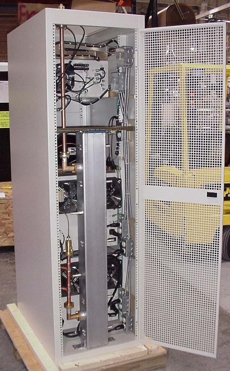
Click to zoom
Application Details
- Equipment Class
- TBC - Licensed Broadcast Station Transmitter
- Date of Grant
- Mar 07, 2004
- Application Purpose
- Original Equipment
- Date of Application
- Jan 15, 2004
- Equipment Note
- 2000-Watt UHF Translator
- Frequency Range
- 470.00000000 - 860.00000000
- Company
- UBS-Axcera
- Country
- United States
Documents & Files
Document Text
Text extracted from the exhibit documents filed with the FCC. Open a document above to read the original.
Users Manual
INSTRUCTION MANUAL INNOVATOR LX SERIES UHF ANALOG DRIVER/UHF TRANSLATOR AXCERA, LLC 103 FREEDOM DRIVE P.O. BOX 525 LAWRENCE, PA 15055-0525 USA (724) 873-8100 • FAX (724) 873-8105 www.axcera.com • [email protected] Analog UHF Driver/Translator Table of Contents LX Series, Rev. 0 August 29, 2003 i TABLE OF CONTENTS SECTION PAGE CHAPTER 1 INTRODUCTION 1.1 Manual Overview............................................................................1-1 1.2 Assembly Designation Numbers.........................................................1-1 1.3 Safety...........................................................................................1-1 1.4 Maintenance..................................................................................1-2 1.5 Material Return Procedure.................................................................1-2 1.6 Limited One-Year Warranty for Axcera Products....................................1-3 CHAPTER 2 SYSTEM DESCRIPTION & REMOTE CONTROL CONNECTIONS 2.1 System Overview...........................................................................2-1 2.1.1 Receiver Tray........................................................................2-2 2.1.2 IF Processor Module................................................................2-3 2.1.3 LO/Upconverter Module...........................................................2-5 2.1.4 Control & Monitoring/Power Supply Module..................................2-7 2.1.5 Power Amplifier Module...........................................................2-8 2.1.6 RF Output Assemblies..............................................................2-9 2.2 Control and Status..........................................................................2-9 2.2.1 Front Panel LCD Display Screen................................................2-10 2.3 System Operation..........................................................................2-10 2.3.1 Principles of Operation............................................................2-11 2.4 Customer Remote Connections.........................................................2-12 CHAPTER 3 SITE CONSIDERATIONS, INSTALLATION AND SETUP PROCEDURES 3.1 Site Considerations..........................................................................3-1 3.2 Unpacking the Chassis w/Modules and Receiver Tray..............................3-4 3.3 Installing the Chassis w/Modules and Receiver Tray...............................3-4 3.4 AC Input.......................................................................................3-6 3.5 Setup and Operation........................................................................3-6 3.5.1 Input Connections..................................................................3-7 3.5.2 Front Panel Screens for the Exciter/Amplifier Chassis Assembly.......3-9 CHAPTER 4 CIRCUIT DESCRIPTIONS 4.1 Receiver Tray.................................................................................4-1 4.1.1 50-Ohm Filter........................................................................4-1 4.1.2 Dual Stage Amplifier Assembly..................................................4-1 4.1.3 Channel Filter........................................................................4-1 4.1.4 Downconverter Amplifier Assembly............................................4-2 4.1.5 Channel Oscillator Assembly.....................................................4-2 4.1.6 x8, x2, x4 Multiplier Board.......................................................4-2 4.1.7 L.O. Filter.............................................................................4-2 4.1.8 IF Filter/ALC Board.................................................................4-2 4.1.9 SAW Board (Optional).............................................................4-2 4.1.10 IF Amplifier Board (Optional)...................................................4-3 4.1.11 IF Filter/Limiter Board (Optional).............................................4-3 4.1.12 IF PLL Board (Optional)..........................................................4-3 4.1.13 IF Carrier Oven Oscillator (Optional).........................................4-3 Analog UHF Driver/Translator Table of Contents LX Series, Rev. 0 August 29, 2003 ii TABLE OF CONTENTS - (Continued) SECTION .........................................................................................PAGE 4.1.14 +/- 12V Power Supply Board...................................................4-4 4.2 IF Processor Module.........................................................................4-4 4.2.1 IF Processor Board..................................................................4-4 4.3 LO/Upconverter Module...................................................................4-10 4.3.1 UHF Generator Board.............................................................4-10 4.3.2 UHF Filters...........................................................................4-11 4.3.3 LO/Upconverter Board............................................................4-11 4.4 Control Monitoring/Power Supply Module............................................4-15 4.4.1 Power Protection Board...........................................................4-16 4.4.2 Control Board.......................................................................4-16 4.4.3 Switch Board........................................................................4-19 4.4.4 Switching Power Supply Assembly............................................4-19 4.5 Power Amplifier Module Assembly......................................................4-19 4.5.1 1-Watt Amplifier Module Assembly............................................4-19 4.5.2 1-Watt UHF Amplifier Board.....................................................4-19 4.5.3 40 Watt UHF Amplifier Assembly...............................................4-20 4.5.4 UHF Module Assembly, RF Module Pallet.....................................4-20 4.5.5 Coupler Board Assembly.........................................…
Text truncated - open the document above for the full version.
Users Manual
INSTRUCTION MANUAL Innovator LX Series Power Amplifier Assembly AXCERA, LLC 103 FREEDOM DRIVE P.O. BOX 525 LAWRENCE, PA 15055-0525 USA (724) 873-8100 • FAX (724) 873-8105 www.axcera.com • [email protected] LX Series Power Amplifier Assembly Table of Contents LX Series, Rev. 0 November 25, 2003 i TABLE OF CONTENTS CHAPTER 1 INTRODUCTION SECTION PAGE 1.1 Manual Overview............................................................................1-1 1.2 Assembly Designation Numbers.........................................................1-1 1.3 Safety...........................................................................................1-1 1.4 Maintenance..................................................................................1-2 1.5 Material Return Procedure.................................................................1-2 1.6 Limited One-Year Warranty for Axcera Products....................................1-3 CHAPTER 2 SYSTEM DESCRIPTION & REMOTE CONTROL CONNECTIONS 2.1 LX Series Power Amplifier Assembly Overview......................................2-1 2.1.1 Power Amplifier Module, 250 Watt.............................................2-1 2.1.2 Power Supply Module Assembly.................................................2-3 2.1.3 Front Panel LCD Display Screens...............................................2-3 2.2 System Operation...........................................................................2-3 2.2.1 Principles of Operation.............................................................2-4 2.3 Customer Remote Connections..........................................................2-5 CHAPTER 3 SITE CONSIDERATIONS, INSTALLATION AND SETUP PROCEDURES 3.1 Site Considerations..........................................................................3-1 3.2 Unpacking the Chassis w/Modules, bandpass and trap filters....................3-4 3.3 Installing the Chassis w/Modules and filters..........................................3-4 3.4 AC Input.......................................................................................3-5 3.5 Setup and Operation........................................................................3-5 3.5.1 Input Connections..................................................................3-5 3.5.2 Front Panel Screens for the Exciter/Amplifier Chassis Assembly.......3-7 3.5.3 Initial Turn On......................................................................3-14 CHAPTER 4 CIRCUIT DESCRIPTIONS 4.1 Power Amplifier Module....................................................................4-1 4.1.1 UHF Phase/Gain Board.............................................................4-1 4.1.2 150 Watt Driver Pallet Assembly................................................4-1 4.1.3 150 Watt Driver, Dual Output Board...........................................4-1 4.1.4 UHF Module Assembly, RF Module Pallet, Philips...........................4-2 4.1.5 2 Way UHF Combiner Assembly.................................................4-2 4.1.6 Amplifier Control Board............................................................4-3 4.2 Power Supply Assembly....................................................................4-5 CHAPTER 5 DETAILED ALIGNMENT PROCEDURES 5.1 Module Replacement........................................................................5-1 5.1.1 Initial Test Setup....................................................................5-1 5.2 Innovator LX Series Exciter/Amplifier Chassis Assembly..........................5-2 5.2.1 Linearity Correction Adjustment................................................5-3 5.2.2 Frequency Response Delay Equalization Adjustment......................5-4 5.2.3 Calibration of Forward Output Power Level...................................5-4 5.2.4 Calibration of Reflected Output Power Level.................................5-5 5.3 Bandpass Filter Assembly.................................................................5-5 LX Series Power Amplifier Assembly Table of Contents LX Series, Rev. 0 November 25, 2003 ii TABLE OF CONTENTS - (Continued) 5.4 UHF Trap Filter Assembly..................................................................5-5 5.4.1 The Effects of Tuning the Output Trap Filter.................................5-6 APPENDICES APPENDIX A INNOVATOR LX SERIES SPECIFICATIONS APPENDIX B DRAWINGS AND PARTS LISTS LX Series Power Amplifier Assembly Table of Contents LX Series, Rev. 0 iii LIST OF FIGURES FIGURE PAGE 3-1 1 kW Minimum Ventilation Configuration.......................................3-4 3-2 Front and Rear View Reconnection Drawing...................................3-5 3-3 Rear View of LX Series Translator................................................3-6 4-1 UHF Amplifier Module, 250 Watts.................................................4-2 5-1 Typical Red Field Spectrum.........................................................5-4 LX Series Power Amplifier Assembly Table of Contents LX Series, Rev. 0 iv LIST OF TABLES TABLE PAGE 2-1 LX Series Power Amplifier Assemblies...........................................2-1 2-2 Power Amplifier Status Indicators................................................2-3 2-3 Power Amplifier Control Adjustments............................................2-3 2-4 Power Amplifier Sample.............................................................2-3 2-5 Pioneer Chassis Customer Remote Connections.......................2-5 3-1 Rear Chassis Connections for LX Series Translator...........................3-6 3-2 Menu 01 Splash Screen #1.........................................................3-7 3-3 Menu 02 Splash Screen #2.........................................................3-7 3-4 Menu 10 Main Screen................................................................3-7 3-5 Menu 11 Error List Access Screen................................................3-8 3-6 Menu 12 Translator Device Data Access Screen..............................3-8 3-7 Menu 13 Translator Configuration Access Scre…
Text truncated - open the document above for the full version.
External Photos
Axcera-LU2000AL FCC Type Acceptance Report External Photos January 2004 2-1 2. EXTERNAL PHOTOS 2.1 Front view, complete LU2000AL Translator Axcera-LU2000AL FCC Type Acceptance Report External Photos January 2004 2-2 2.2 Rear view, complete Axcera-LU2000AL Translator
ID Label/Location Info
Axcera-LU2000AL FCC Type Acceptance Report ID Label/Location Info January 2004 1-1 1. ID LABEL/LOCATION INFO 1.1 Front Panel FCC Label 1.2 Rear Panel Manufacturer’s Label Axcera-LU2000AL FCC Type Acceptance Report ID Label/Location Info January 2004 1-2 1.3 Front view, complete Axcera-LU2000AL Translator with FCC Label Axcera-LU2000AL FCC Type Acceptance Report ID Label/Location Info January 2004 1-3 1.4 Rear view, complete Axcera-LU2000AL Translator Axcera-LU2000AL FCC Type Acceptance Report ID Label/Location Info January 2004 1-4 Rear view, Axcera-LU2000AL Translator with Manufacturer’s Label.
Internal Photos
Axcera-LU2000AL FCC Type Acceptance Report Internal Photos January 2004 6-1 6. INTERNAL PHOTOS 6.1 Front view – Chassis Assembly (Exciter) Axcera-LU2000AL FCC Type Acceptance Report Internal Photos January 2004 6-2 6.2 Side view - IF Processor Assembly (Exciter) 6.3 Side view - L.O. Upconverter Assembly (Exciter) Axcera-LU2000AL FCC Type Acceptance Report Internal Photos January 2004 6-3 6.4 Side view - Control / Power Supply Assembly (Exciter) 6.5 Side view - Power Amplifier Assembly (Exciter) Axcera-LU2000AL FCC Type Acceptance Report Internal Photos January 2004 6-4 6.6 Front view – Chassis Assembly (External Power Amplifier) 6.7 Side view - Power Amplifier Assembly (External Power Amplifier) Axcera-LU2000AL FCC Type Acceptance Report Internal Photos January 2004 6-5 6.8 Side view – Power Supply Assembly (External Power Amplifier) 6.9 Side view – 4-Way Combiner Assembly (External Power Amplifier) Axcera-LU2000AL FCC Type Acceptance Report Internal Photos January 2004 6-6 6.10 Top view, Receiver Tray
Operational Description
Axcera-LU2000AL FCC Type Acceptance Report Operational Description January 2004 8-1 8. OPERATIONAL DESCRIPTION - MODEL Axcera-LU2000AL 8.1 General Description The LU2000AL is a complete 2000-watt UHF solid-state, internally diplexed television translator. It operates at a nominal visual output power of 2000 watts peak sync and an average aural output power of 200 watts, at an A/V ratio of 10 dB, 10% sound. 8.2 Technical Specifications Type of Emissions: Visual .......................................................................... 5M75C3F Aural ............................................................................250KF3E Frequency Range....................... 470 MHz to 860 MHz (any 6-MHz channel) Output Power Visual .........................................................2000 watts peak sync Aural .............................................................. 200 watts average Maximum Power Rating Visual ....................................................... 2000 watts peak visual Aural ...................................................... 200 watts average aural Power Consumption .............................................................. 6700 watts 8.3 Performance Specifications Visual Performance Operating Frequency Range ...................................... 470 MHz to 860 MHz RF output - Nominal: Power .........................................................2000 watts peak sync Impedance .................................................................... 50 ohms Connector..................................................................... 7/8” EIA Visual Sideband Response: -1.25 MHz and below ........................................................... -20B -0.75 to -0.5 MHz..................................................... +0.5, -2.0dB -0.5 MHz to +3.58 MHz....................................................±0.5 dB 3.58 MHz to 4.18 MHz.............................................. +0.5, -1.0 dB Variation of Frequency Response with Brightness...........................±0.5 dB Differential Phase ............................................................................ ±3° Incidental Phase Modulation.............................................................. ±3° Differential Gain .............................................................................. 5% Low Frequency Linearity ................................................................... 5% Intermodulation Products .............................................. -52 dB (red field) Output Variation (Over 1 Frame) ....................................................... 2% Regulation of Output........................................................................ 3% Signal-to-Noise Ratio ................................................................. 55 dB Axcera-LU2000AL FCC Type Acceptance Report Operational Description January 2004 8-2 2t K-Factor.................................................................................. 2% Harmonic Radiation .....................................................................-60 dB Spurious (>3 MHz from channel edge) ...........................................-50 dB Carrier Frequency Stability....................................................... ±1000 Hz Noise Figure w/Input Preamp .................................................3 dB (Max.) Input Dynamic Range (no Preamp) .................................. --60 to -15 dBm Aural Performance RF Output – Nominal Power......................................................................... 200 watts Impedance .................................................................... 50 ohms Connector..................................................................... 7/8” EIA Electrical Requirements Power Line Voltage................................................... 230 volts, 50/60 Hz Power Consumption .............................................................. 6700 watts Environmental Maximum Altitude ..................................................................8,500 feet Operational Temperature Range ...........................................0°C to +50°C Mechanical Dimensions: Width ..........................................................................22 inches Depth ..........................................................................34 inches Height..........................................................................55 inches Weight ............................................................................ 550 lbs 8.4. System Overview The LU2000AL (1303828) is made up of the (3) trays listed in Table 8-1. Table 8-1. LU2000AL Major Trays and Assemblies MAJOR ASSEMBLY DESIGNATOR TRAY/ASSEMBLY NAME DRAWING NUMBER A1 Receiver 1265-1100 A2 UHF Exciter 1303268 A3, A4 External Amplifier Assembly 1303828 The (A2) UHF Exciter can operate using a 45.75 MHz IF carrier from either the (A1) Receiver tray’s output, or that from a Modulator tray. Both of these carriers must be diplexed with a 41.25 MHz aural carrier, at an A/V ratio not to exceed –10dB. Axcera-LU2000AL FCC Type Acceptance Report Operational Description January 2004 8-3 8.4.1 Receiver Tray The RF Input to the Tray, (-61 dBm to -26 dBm in Level), is fed through J1 to the input 50Ω Filter or through J5 to the 75Ω input Filter, which are of a double tuned design that is adjusted to the desired Input UHF or VHF Channel Frequency. Note: If the input signal is greater then -25dBm, an attenuator should be used to limit the level to -25dBm. +12 VDC, for use by an (Optional) external Preamplifier Assembly, connects to the filter through F1 a 1 Amp Fuse. This +12 VDC is DC Multiplexed onto the input signal cable from the Preamplifier. DS1 a Red LED located on TB1 in the Tray will be lit if the +12 VDC is present on the input cable. If a Preamplifier is not used, F1 should be removed and DS1 should not be lit. The signal is next amplified +12 dB to approximately the -49 to -4 dBm level by a low noise amplifier located on the Dual Sta…
Text truncated - open the document above for the full version.
Parts List/Tune Up Info
Axcera-LU2000AL FCC Type Acceptance Report Parts List/Tune-up Info January 2004 7-1 7. PARTS LIST/TUNE-UP INFO 7.1 Parts List The translator, can be subdivided as follows: Receiver Tray: • VHF filter • Dual stage amplifier board • Channel oscillator Assembly • Channel oscillator multiplier board • Downconverter/amplifier board • IF filter/ALC board • SAW filter amplifier board • Power supply board Exciter Tray: • IF Processor Module • L.O. / Upconverter Module • Control & Monitoring / Power Supply Module • Power Amplifier Module External Amplifier Trays: • 4-Way Splitter (Qty of 2) • Power Amplifier Module (Qty of 8) • Power Supply Module (Qty of 4) • 4-Way Combiner (Qty of 2) 7.2 Tune-up Information The LU2000AL translator was aligned at the factory and should not require additional alignments to achieve normal operation. The UHF/VHF Receiver Tray w/(Optional) Frequency Correction selects the desired UHF or VHF On Channel Input Signal and converts it to a Combined IF Signal of 45.75 MHz Visual + 41.25 MHz Aural. The Tray also has provisions for a Frequency Correction Option that consists of a VCXO Channel Oscillator Assembly with a PLL Circuit which maintains an exact IF Output Frequency, over the capture range of the PLL circuit, even if the Input UHF or VHF Frequency may vary. 7.2.1 RF Input Signal Path (Receiver) The RF Input to the Tray, (-61 dBm to -16 dBm in Level), is fed through J1 for 50Ω to (A7) the input 50Ω Filter, DC Multiplexed (1035-1204 UHF, 1035-1902 VHF LB or 2065-1024 VHF HB) or through J5 for 75Ω to (A7) the 75Ω input Filter, DC Multiplexed (1035-1207 UHF, 1035-1903 VHF LB or 2065-1023 VHF HB), which is of a double tuned design that is adjusted to the desired Input UHF or VHF Channel Frequency. Note: If the input signal is greater then -25dBm, an attenuator should be used to limit the level to -25dBm. +12 VDC, for use by an (Optional) external Preamplifier Assembly, connects to the filter through F1 a 1 Amp Fuse. This +12 VDC is DC Multiplexed onto the input signal cable from the Preamplifier. DS1 a Red LED located on TB1 in the Tray will be lit if the +12 VDC is present on the input cable. If a Preamplifier is not used, F1 should be removed and DS1 should not be lit. Axcera-LU2000AL FCC Type Acceptance Report Parts List/Tune-up Info January 2004 7-2 The signal is next amplified +12 dB to approximately the -49 to -4 dBm level by a low noise amplifier located on (A8-A1) the Dual Stage Amplifier Board (1227-1501) that is contained in (A8) the Dual Stage Amplifier Assembly (1227-1503). The board has approximately +13 dB or +26 dB of gain, depending on whether Jumper W1 on J5 is in place. The signal is then filtered in (A9) a Channel Filter (1007-1101 UHF, 1034-1202 VHF LB or 2065-1000 VHF HB) and then applied back to (A8-A1) the Dual Stage Board where the same amplification takes place. Jumper W1 on J7, located on the Dual Stage Board, should be removed if the Receiver Input level is greater than -40dBm. The output is connected to (A10) the Downconverter Amplifier Assembly (1227-1505) that contains (A10-A1) the Downconverter Amplifier Board (1227-1502). The RF, at the -47 dBm to -2 dBm Level, connects to the "R" Input Jack of the Mixer Z1 located on the Downconverter Amplifier Board. 7.2.2 Local Oscillator Signal Path (Receiver) The Local Oscillator Signal is derived from a cut to channel crystal mounted in an oven that is factory set at 45° C. The Oscillator operates at 1/8 for UHF, 1/4 for VHF High Band or 1/2 for VHF Low Band of the desired local oscillator frequency. The crystal is mounted on (A4-A1) the Channel Oscillator Board, Dual Oven (1145-1201), that is part of the Channel Oscillator Assembly (1145-1202). The oscillator circuitry is a modified Colpitts design operating in a separate oven set at 50° C. for improved stability. If the Frequency Correction Option is purchased, the VCXO Channel Oscillator Assembly (1145-1206), which contains the VCXO Channel Oscillator Board (1145-1204), is used in place of the standard Channel Oscillator Assembly, and an AFC voltage from the PLL circuit maintains the frequency of the VCXO. The output of the Channel Oscillator is connected to the (A5-A1) the x8 Multiplier Board (1227-1002) for UHF, the x4 Multiplier Board (1227-1525) for VHF HB or the x2 Multiplier Board (1227-1524) for VHF LB, which is located in (A5) the Multiplier Enclosure (1265- 1125). The proper multiplier board takes the output of the Channel Oscillator (+3 dBm) and multiplies it eight, four or two times by a series of three, two or one x2 Broadband Doublers (2x2x2 = x8), which produces the L.O. signal on the desired frequency needed for the upconversion process. The signal is then amplified to the +16 dBm level. A sample of the multiplied L.O. Signal is fed to a detector circuit, which lights the Green LED DS1 that indicates that the L.O. is present at the Output Jack J2 of the Multiplier Board. This Green LED is seen through a hole in the lid of the Multiplier Assembly and is an indication, when lit, that there is a signal present at the output of the Multiplier Board. The L.O. signal is filtered in (A6) a L.O. Filter 1007-1101 UHF, 2065-1000 VHF HB or 1034-1211 VHF LB) and then sent (+15 dBm) to J2 on (A10-A1) the Downconverter Amplifier Board. The L.O. Input to the Downconverter Amplifier Board is connected thru a 3 dB matching pad to the "L" Input of the Mixer (Z1) at a +12 dBm level. 7.2.3 Combined IF Signal Path (Receiver) The L.O. and the RF signals are mixed in the Mixer Stage of the Downconverter Amplifier Board to produce the desired IF difference frequency at -55 dBm to -10 dBm in level, depending on the RF Input Level. The Combined IF Signal is routed to (A11-A1) the IF Filter/ALC Board (1227-1504), which is mounted in (A11) the IF Filter/ALC Enclosure (1265-1105). The IF Filter/ALC Board contains a Pin Diode Attenuator circuit, which is part of the Automatic Level Control (ALC) that controls the level of the IF Signal to the two stage amplifie…
Text truncated - open the document above for the full version.
Schematics
5 5 4 4 3 3 2 2 1 1 DD CC BB AA -12V +12V VREF +12V -12V +6.8V +6.8V +6.8V +12V -12V +12V -12V VREF +12V VREF +6.8V -12V +12V -12V +12V VREF +6.8V +12V +12V +12V +12V -12V +12V -12V +12V +12V +12V -12V +12V -12V -12V +12V +12V -12V +12V -12V -12V -12V +12V +12V +12V +12V +12V -12V -12V +12V -12V +12V +12V -12V -12V +12V +12V +12V +12V -12V -12V -12V +12V +12V -12V +12V A B J42-G J42-C J42-B J42-D J42-A J42-F C J42-E J42-H J42-J J42-K Axcera REV ECO DATEAPV TITLE THIS PRINT IS THE PROPERTY OF AXCERA, IT SHALL NOT BE COPIED WITHOUT PERMISSION MATERIAL FINISH DWN CHK REL SCALESHEET REV REV ECO DATE APV DWG. NO. --- ----- ----- 1301983 B0 SCH., ANALOG, IF PROCESSOR BD. (1301977) JKF 2/24/03 D1 OF 2 3/6/03 LRT 3/6/03LRT CUTBACK LEVEL CUTBACK ENABLE/DISABLE MOD IF I/P VIDEO LOSS MODULATOR SEL. LOCAL MOD SELECT DISABLE/ ENABLE NOTES: 1) ALL DIODES ARE 1N5711 UNLESS OTHERWISE NOTED. 2) ALL NPN TRANSITORS ARE 2N3904 UNLESS OTHERWISE NOTED. 3) ALL OP AMPS ARE TL074 UNLESS OTHERWISE NOTED. 4) ALL CAPACITORS ARE IN uF UNLESS OTHERWISE NOTED. 5) ALL INDUCTORS ARE IN uH UNLESS OTHERWISE NOTED. 6) ALL RESISTORS ARE 1/8W UNLESS OTHERWISE NOTED. INPUT FAULT FREQ RESP MOD ENABLE BD. BD. IN PHASE OUTPUT QUADRATURE OUTPUT IN PHASE QUADRATURE W13 W 14 THRESHOLD THRESHOLD IN PHASE AMP. ADJ. QUAD AMP. ADJ. J42-7C J42-32B J42-14C J42-24C J42-21C J42-9C CORRECTION ENABLEDISABLE THRESHOLD FULL POWER SET J42-8C J42-16C J42-18C FAULT DETECTOR PIN ATTEN. VOLT W13 ADD ED J36 - J41, L54 - L5 6, W13 -W15, TP5, TP6, & R275, R276, R279 -R 285. R225 & R229 WERE 130 OH M. U14, U18 & U22 WERE MAV-11. ADDED NOTE EXTERNAL CABLE ASSY FOR W13 & W14CON N. JKF B0 W15 (FT PNL) (FT PNL) (FT PNL) (FT PNL) J42-30C (FT PNL) FULL POWER SET EXTERN AL CABLE ASSY. EXTERN AL CABLE ASSY. 2 0110968 9/3/ 03 LRT R214 130 1W C6 .01 R239 20 1/16W U16D TLO74 + 12 - 13 14 - 11 + 4 C155 .1 C159 .01 U24D TLO74 + 12 - 13 14 - 11 + 4 R53 4.7K R242 330 1/16W C145 .01 J33 1 2 3 U19A TLO74 + 3 - 2 1 - 11 + 4 U18 ERA-5 1 3 2 4 R206 5.6 1/16W R59 100 R224 470 S EC P RI T6 T4-1 1 CT 2 34 NC 5 6 L47 .47uH U24C TLO74 + 10 - 9 8 - 11 + 4 R200 51 R50 100 L46 .47uH J30 1 2 3 R223 0 R201 51 R254 130 1W S EC P RI T7 T4-1 1 CT 2 34 NC 5 6 L31 .47 C9 .01 R68 2.7K C149 .01 U20 MAV-11 1 3 2 4 L6 .1 C168 .1 C44 .01 C166 .1 Z1 SCPQ-50 SUM PORT 1 PORT 1 2 GND 3 GND 4 PORT 2 5 50 TERM 6 GND 7 GND 8 U9B + 5 - 6 7 - 11 + 4 L52 .47uH TP5 + C57 10 uF 35V C143 .1 R240 0 R52 2.7K CR19 1N914 C45 .01 L3 .1 J5 1 2 3 J40 1 2 3 R255 110 1W C13 .01 R212 470 C144 .01 J36 1 2 3 R231 5K CW 3 2 1 R221 130 1W R251 22 1/16W R237 22 1/16W C11 .01 C142 .1 C131 .01 R227 68 1/16W L49 4.7 R69 510 R210 100 L4 .27 C8 .01 R258 200 CW 3 2 1 R55 1K C153 .01 R2 470 CR30 1N5711 L7 .47 L30 .47 CR14 L42 4.7 C163 .01 C10 .01 R233 10 TP6 R282 10K 1/10W 1% CR25 1N5711 C141 .01 R244 130 R281 10K 1/10W 1% R216 5K CW 3 2 1 C83 .1 R253 27 CR13 + C81 10 uF 35V R256 68 1/16W R238 200 CW 3 2 1 CR26 1N5711 R4 470 R208 5.6 1/16W C46 .01 R220 51 C1 100pF CR15 1N914 Q4 B 1 C 3 E 2 C124 .1 C84 .1 U19C TLO74 + 10 - 9 8 - 11 + 4 J41 1 2 3 + C80 10 uF 35V R63 47K C162 .01 R218 470 C147 .01 J37 1 2 3 C53 .1 C161 .01 S EC P RI T8 T4-1 1 CT 2 34 NC 5 6 R229 110 1W C146 .01 R249 68 1/16W R128 68K C160 .01 R230 22 1/16W R235 470 Q15 BS170 R279 10K 1/10W 1% R51 10K + C47 10 uF 35V R137 510 L51 .47uH VR3 6.8V L5 .27 C48 .1 R121 2.2K C165 .01 J31 1 2 3 R261 470 DS5 CR31 1N5711 R57 100K R257 0 CR17 R65 6.8K L43 4.7 Q2 B 1 E 2 C 3 CR1 1N5767 Z2 ADP-2-1W S PORT 1 N.C. 2 PORT 1 3 PORT 2 4 N.C. 5 GND 6 C139 .1 R246 180 1/16W CR20 1N914 C172 .01 L44 4.7 R236 470 R209 5.6 1/16W L18 .47 C50 4.7pF Q12 BS170 R48 100 U19B TLO74 + 5 - 6 7 - 11 + 4 U19D TLO74 + 12 - 13 14 - 11 + 4 W2 C123 .1 R250 180 1/16W R247 22 1/16W C132 180pF R71 5K CW 3 2 1 U1 MAV-11 1 3 2 4 CR27 1N5711 C150 .01 L2 .27 + C52 10 uF 35V R130 1K R222 180 1/16W R265 47K TP1 R232 560 1/16W J29 1 2 3 R54 2K 1/2W R285 0 R219 0 U9D + 12 - 13 14 - 11 + 4 R132 1.5K R217 10 C133 130pF C51 .001 L50 .47uH C135 51 pF VR2 1N4733A U17 MAV-11 1 3 2 4 C130 .01 L48 4.7 R211 5K CW 3 2 1 R243 3K 1/16W R9 2.7K R264 10K 1/16W U9A + 3 - 2 1 - 1…
Text truncated - open the document above for the full version.
Contact Information
Applicant
David Hewitt(Engineering Manager)
Technical Contact
AxceraLance R Trussa
[email protected]724-873-8100
103 Freedom Drive · Lawrence, Pennsylvania · United States
Non-Technical Contact
AxceraJames C Mounts
[email protected]724-873-8100
Technical Specifications
| # | Rule Parts | Frequency Range | Power Output | Emission | Tolerance |
|---|---|---|---|---|---|
| 2 | 74 | 470 MHz - 860 MHz | 2000 W | 5M75C3F | 1000 Hz |
Other Applications from UBS-Axcera

OUSCU0TD-5-UBS
Mar 27, 2014200W UHF Digital Transmitter
Equipment Class
TBC - Licensed Broadcast Station Transmitter
OUSCL1TC-4
Sep 17, 2013400-Watt, 1.6 GHz DVB-H Transmitter
Equipment Class
TNB - Licensed Non-Broadcast Station Transmitter
OUSCLV2TD-4
Aug 22, 2013Low Band VHF Digital Broadcast Transmitter
Equipment Class
TBC - Licensed Broadcast Station Transmitter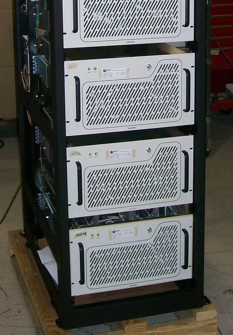
OUSCHV4TD
Jun 14, 20123000-Watt VHF Digital Transmitter
Equipment Class
TBC - Licensed Broadcast Station Transmitter
OUSCU0TD-5
Dec 14, 2011200 Watt UHF Digital Transmitter
Equipment Class
TBC - Licensed Broadcast Station Transmitter