OUSLU2000AT2000-Watt UHF Transmitter
UBS-Axcera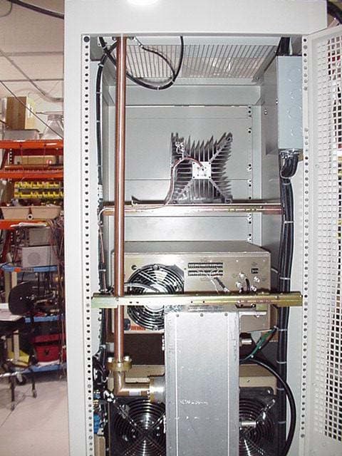
Click to zoom
Application Details
- Equipment Class
- TBC - Licensed Broadcast Station Transmitter
- Date of Grant
- Apr 27, 2004
- Application Purpose
- Original Equipment
- Date of Application
- Mar 29, 2004
- Equipment Note
- 2000-Watt UHF Transmitter
- Frequency Range
- 470.00000000 - 860.00000000
- Company
- UBS-Axcera
- Country
- United States
Documents & Files
Document Text
Text extracted from the exhibit documents filed with the FCC. Open a document above to read the original.
Users Manual
INSTRUCTION MANUAL INNOVATOR LX SERIES UHF Analog Driver/Transmitter AXCERA, LLC 103 FREEDOM DRIVE P.O. BOX 525 LAWRENCE, PA 15055-0525 USA (724) 873-8100 • FAX (724) 873-8105 www.axcera.com • [email protected] UHF Analog Driver/Transmitter Table of Contents LX Series, Rev. 0 October 31, 2003 i TABLE OF CONTENTS SECTION PAGE CHAPTER 1 INTRODUCTION 1.1 Manual Overview............................................................................1-1 1.2 Assembly Designation Numbers.........................................................1-1 1.3 Safety...........................................................................................1-1 1.4 Maintenance..................................................................................1-2 1.5 Material Return Procedure.................................................................1-2 1.6 Limited One-Year Warranty for Axcera Products....................................1-3 CHAPTER 2 SYSTEM DESCRIPTION & REMOTE CONTROL CONNECTIONS 2.1 System Overview...........................................................................2-1 2.1.1 Modulator Module (not used in a translator system).......................2-1 2.1.2 IF Processor Module................................................................2-3 2.1.3 LO/Upconverter Module...........................................................2-5 2.1.4 Control & Monitoring/Power Supply Module..................................2-7 2.1.5 Power Amplifier Module, 10-100W transmitter..............................2-8 2.1.5.1 Driver Amplifier Module, used with high power transmitters....2-9 2.1.6 RF Output Assemblies.............................................................2-11 2.2 Control and Status.........................................................................2-11 2.2.1 Front Panel LCD Display Screen................................................2-11 2.3 System Operation..........................................................................2-12 2.3.1 Principles of Operation............................................................2-12 2.4 Customer Remote Connections.........................................................2-14 CHAPTER 3 SITE CONSIDERATIONS, INSTALLATION AND SETUP PROCEDURES 3.1 Site Considerations..........................................................................3-1 3.2 Unpacking the Chassis w/Modules, bandpass and trap filters....................3-4 3.3 Installing the Chassis w/Modules and filters..........................................3-4 3.4 AC Input.......................................................................................3-5 3.5 Setup and Operation........................................................................3-5 3.5.1 Input Connections..................................................................3-5 3.5.2 Front Panel Screens for the Exciter/Amplifier Chassis Assembly.......3-7 3.5.3 Initial Turn On......................................................................3-14 CHAPTER 4 CIRCUIT DESCRIPTIONS 4.1 Modulator Module (not used in a translator system)...............................4-1 4.1.1 Analog Modulator Board...........................................................4-1 4.2 IF Processor Module.........................................................................4-6 4.2.1 IF Processor Board..................................................................4-6 4.3 LO/Upconverter Module...................................................................4-11 4.3.1 UHF Generator Board.............................................................4-12 4.3.2 UHF Filters...........................................................................4-13 4.3.3 LO/Upconverter Board............................................................4-13 4.4 Control Monitoring/Power Supply Module............................................4-17 4.4.1 Power Protection Board...........................................................4-17 4.4.2 Control Board.......................................................................4-18 4.4.3 Switch Board........................................................................4-20 4.4.4 Switching Power Supply Assembly............................................4-20 UHF Analog Driver/Transmitter Table of Contents LX Series, Rev. 0 October 31, 2003 ii TABLE OF CONTENTS - (Continued) SECTION PAGE 4.5 Power Amplifier Module Assembly used in 10-100 Watt transmitters.........4-21 4.5.1 1-Watt Amplifier Module Assembly............................................4-21 4.5.2 1-Watt UHF Amplifier Board.....................................................4-21 4.5.3 40-Watt UHF Amplifier Assembly..............................................4-21 4.5.4 UHF Module Assembly, RF Module Pallet.....................................4-22 4.5.5 Coupler Board Assembly.........................................................4-23 4.5.6 Amplifier Control Board...........................................................4-23 4.5.7 Band-pass and Trap Filter.......................................................4-25 4.6 OR Driver Amplifier Module Assembly used in high power transmitters......4-25 4.6.1 1-Watt Amplifier Module Assembly............................................4-25 4.6.2 1-Watt UHF Amplifier Board.....................................................4-26 4.6.3 40-Watt UHF Amplifier Assembly..............................................4-26 4.6.4 Coupler Board Assembly.........................................................4-26 4.6.5 Amplifier Control Board...........................................................4-27 CHAPTER 5 DETAILED ALIGNMENT PROCEDURES 5.1 Module Replacement........................................................................5-1 5.1.1 Initial Test Setup....................................................................5-1 5.2 LU Series Exciter/Amplifier Chassis Assembly........................................5-2 5.2.1 Linearity Correction Adjustment................................................5-3 5…
Text truncated - open the document above for the full version.
Users Manual
INSTRUCTION MANUAL Innovator LX Series Power Amplifier Assembly AXCERA, LLC 103 FREEDOM DRIVE P.O. BOX 525 LAWRENCE, PA 15055-0525 USA (724) 873-8100 • FAX (724) 873-8105 www.axcera.com • [email protected] LX Series Power Amplifier Assembly Table of Contents LX Series, Rev. 0 November 25, 2003 i TABLE OF CONTENTS CHAPTER 1 INTRODUCTION SECTION PAGE 1.1 Manual Overview............................................................................1-1 1.2 Assembly Designation Numbers.........................................................1-1 1.3 Safety...........................................................................................1-1 1.4 Maintenance..................................................................................1-2 1.5 Material Return Procedure.................................................................1-2 1.6 Limited One-Year Warranty for Axcera Products....................................1-3 CHAPTER 2 SYSTEM DESCRIPTION & REMOTE CONTROL CONNECTIONS 2.1 LX Series Power Amplifier Assembly Overview......................................2-1 2.1.1 Power Amplifier Module, 250 Watt.............................................2-1 2.1.2 Power Supply Module Assembly.................................................2-3 2.1.3 Front Panel LCD Display Screens...............................................2-3 2.2 System Operation...........................................................................2-3 2.2.1 Principles of Operation.............................................................2-4 2.3 Customer Remote Connections.....................................................2-5 CHAPTER 3 SITE CONSIDERATIONS, INSTALLATION AND SETUP PROCEDURES 3.1 Site Considerations..........................................................................3-1 3.2 Unpacking the Chassis w/Modules, bandpass and trap filters....................3-4 3.3 Installing the Chassis w/Modules and filters..........................................3-4 3.4 AC Input.......................................................................................3-5 3.5 Setup and Operation........................................................................3-5 3.5.1 Input Connections..................................................................3-5 3.5.2 Front Panel Screens for the Exciter/Amplifier Chassis Assembly.......3-7 3.5.3 Initial Turn On......................................................................3-14 CHAPTER 4 CIRCUIT DESCRIPTIONS 4.1 Power Amplifier Module....................................................................4-1 4.1.1 UHF Phase/Gain Board.............................................................4-1 4.1.2 150 Watt Driver Pallet Assembly................................................4-1 4.1.3 150 Watt Driver, Dual Output Board...........................................4-1 4.1.4 UHF Module Assembly, RF Module Pallet, Philips...........................4-2 4.1.5 2 Way UHF Combiner Assembly.................................................4-2 4.1.6 Amplifier Control Board............................................................4-3 4.2 Power Supply Assembly....................................................................4-5 CHAPTER 5 DETAILED ALIGNMENT PROCEDURES 5.1 Module Replacement........................................................................5-1 5.1.1 Initial Test Setup....................................................................5-1 5.2 Innovator LX Series Exciter/Amplifier Chassis Assembly..........................5-2 5.2.1 Linearity Correction Adjustment................................................5-3 5.2.2 Frequency Response Delay Equalization Adjustment......................5-4 5.2.3 Calibration of Forward Output Power Level...................................5-4 5.2.4 Calibration of Reflected Output Power Level.................................5-5 5.3 Bandpass Filter Assembly.................................................................5-5 LX Series Power Amplifier Assembly Table of Contents LX Series, Rev. 0 November 25, 2003 ii TABLE OF CONTENTS - (Continued) 5.4 UHF Trap Filter Assembly..................................................................5-5 5.4.1 The Effects of Tuning the Output Trap Filter.................................5-6 APPENDICES APPENDIX A INNOVATOR LX SERIES SPECIFICATIONS APPENDIX B DRAWINGS AND PARTS LISTS LX Series Power Amplifier Assembly Table of Contents LX Series, Rev. 0 iii LIST OF FIGURES FIGURE PAGE 3-1 1 kW Minimum Ventilation Configuration.......................................3-4 3-2 Front and Rear View Reconnection Drawing...................................3-5 3-3 Rear View of LX Series Transmitter..............................................3-6 4-1 UHF Amplifier Module, 250 Watts.................................................4-2 5-1 Typical Red Field Spectrum.........................................................5-4 LX Series Power Amplifier Assembly Table of Contents LX Series, Rev. 0 iv LIST OF TABLES TABLE PAGE 2-1 LX Series Power Amplifier Assemblies...........................................2-1 2-2 Power Amplifier Status Indicators................................................2-3 2-3 Power Amplifier Control Adjustments............................................2-3 2-4 Power Amplifier Sample.............................................................2-3 2-5 Pioneer Chassis Customer Remote Connections.......................2-5 3-1 Rear Chassis Connections for LX Series Transmitter.........................3-6 3-2 Menu 01 Splash Screen #1.........................................................3-7 3-3 Menu 02 Splash Screen #2.........................................................3-7 3-4 Menu 10 Main Screen................................................................3-7 3-5 Menu 11 Error List Access Screen................................................3-8 3-6 Menu 12 Transmitter Device Data Access Screen............................3-8 3-7 Menu 13 Transmitter Configuration Access Screen.....…
Text truncated - open the document above for the full version.
External Photos
External Photos In order to minimize the number of uploaded exhibit files, this information has been included in the uploaded file “Compiled Report Part 1 – LU2000AT.pdf”
External Photos
Axcera-LU2000AT FCC Type Acceptance Report External Photos March 2004 2-1 2. EXTERNAL PHOTOS 2.1 Front view, complete LU2000AT Transmitter Axcera-LU2000AT FCC Type Acceptance Report External Photos March 2004 2-2 2.2 Rear view, Axcera-LU2000AT Transmitter (upper cabinet view) Axcera-LU2000AT FCC Type Acceptance Report External Photos March 2004 2-3 2.3 Rear view, Axcera-LU2000AT Transmitter (lower cabinet view)
ID Label/Location Info
ID / Label Location Info In order to minimize the number of uploaded exhibit files, this information has been included in the uploaded file “Compiled Report Part 1 – LU2000AT.pdf”
ID Label/Location Info
Axcera-LU2000AT FCC Type Acceptance Report ID Label/Location Info March 2004 1-1 1. ID LABEL/LOCATION INFO 1.1 Front Panel FCC Label 1.2 Rear Panel Manufacturer’s Label Axcera-LU2000AT FCC Type Acceptance Report ID Label/Location Info March 2004 1-2 1.3 Front view, complete Axcera-LU2000AT Transmitter with FCC Label Axcera-LU2000AT FCC Type Acceptance Report ID Label/Location Info March 2004 1-3 1.4 Rear view, Axcera-LU2000AT Transmitter with Manufacturer’s Label.
Internal Photos
Internal Photos In order to minimize the number of uploaded exhibit files, this information has been included in the uploaded file “Compiled Report Part 2 – LU2000AT.pdf”
Internal Photos
Axcera-LU2000AT FCC Type Acceptance Report Internal Photos March 2004 6-1 6. INTERNAL PHOTOS 6.1 Front view – Chassis Assembly (Exciter) 6.2 Side view - Modulator Assembly (Exciter) Axcera-LU2000AT FCC Type Acceptance Report Internal Photos March 2004 6-2 6.3 Side view - IF Processor Assembly (Exciter) 6.4 Side view - L.O. Upconverter Assembly (Exciter) Axcera-LU2000AT FCC Type Acceptance Report Internal Photos March 2004 6-3 6.5 Side view - Control / Power Supply Assembly (Exciter) 6.6 Side view - Power Amplifier Assembly (Exciter) Axcera-LU2000AT FCC Type Acceptance Report Internal Photos March 2004 6-4 6.7 Front view – Chassis Assembly (External Power Amplifier) x2 6.8 Side view - Power Amplifier Assembly (External Power Amplifier) x8 Axcera-LU2000AT FCC Type Acceptance Report Internal Photos March 2004 6-5 6.9 Side view – Power Supply Assembly (External Power Amplifier) x4 6.10 Side view – 4-Way Combiner Assembly (External Power Amplifier) x2
Operational Description
Operational Description In order to minimize the number of uploaded exhibit files, this information has been included in the uploaded file “Compiled Report Part 2 – LU2000AT.pdf”
Operational Description
Axcera-LU2000AT FCC Type Acceptance Report Operational Description March 2004 8-1 8. OPERATIONAL DESCRIPTION - MODEL Axcera-LU2000AT 8.1 General Description The LU2000AT is a complete 2000-watt UHF solid-state, internally diplexed television transmitter. It operates at a nominal visual output power of 2000 watts peak sync and an average aural output power of 200 watts, at an A/V ratio of 10 dB, 10% sound. 8.2 Technical Specifications Type of Emissions: Visual .......................................................................... 5M75C3F Aural ............................................................................250KF3E Frequency Range....................... 470 MHz to 860 MHz (any 6-MHz channel) Output Power Visual .........................................................2000 watts peak sync Aural .............................................................. 200 watts average Maximum Power Rating Visual ....................................................... 2000 watts peak visual Aural ...................................................... 200 watts average aural Power Consumption .............................................................. 6700 watts 8.3 Performance Specifications Visual Performance Operating Frequency Range ...................................... 470 MHz to 860 MHz RF output - Nominal: Power .........................................................2000 watts peak sync Impedance .................................................................... 50 ohms Connector..................................................................... 7/8” EIA Visual Sideband Response: -1.25 MHz and below ........................................................... -20B -0.75 to -0.5 MHz..................................................... +0.5, -2.0dB -0.5 MHz to +3.58 MHz....................................................±0.5 dB 3.58 MHz to 4.18 MHz.............................................. +0.5, -1.0 dB Variation of Frequency Response with Brightness...........................±0.5 dB Differential Phase ............................................................................ ±3° Incidental Phase Modulation.............................................................. ±3° Differential Gain .............................................................................. 5% Low Frequency Linearity ................................................................... 5% Intermodulation Products .............................................. -52 dB (red field) Output Variation (Over 1 Frame) ....................................................... 2% Regulation of Output........................................................................ 3% Axcera-LU2000AT FCC Type Acceptance Report Operational Description March 2004 8-2 Signal-to-Noise Ratio ................................................................. 55 dB 2t K-Factor.................................................................................. 2% Harmonic Radiation .....................................................................-60 dB Spurious (>3 MHz from channel edge) ...........................................-50 dB Carrier Frequency Stability....................................................... ±1000 Hz Aural Performance Frequency Deviation Capability (Transmitters) ............................. ±75 kHz Distortion .....................................................................................0.5% FM Noise ....................................................................................-60 dB AM Noise ....................................................................................-55 dB Visual to Aural Separation ......................................... 4.5 MHz, ±100 Hz Composite Audio Input (Multi-channel sound - Transmitters) Input Level ........................................................1V peak, nominal Input Impedance.......................................... 75 ohms, unbalanced Frequency Range: ±0.1 dB Response.................................................50 Hz to 50 kHz ±0.5 dB Response ............................................30 Hz to 120 kHz Monaural Audio Input (Transmitters): Input Level ............................................................ 0 to +10 dBm Input Impedance............................................ 600 ohms, balanced Frequency Range (±0.5 dB resp.) ..........................30 Hz to 15 kHz Pre-emphasis..................................................................... 75 uS Subcarrier Audio Input (Transmitters): Input Level ........................................................1V peak, nominal Input Impedance.......................................... 75 ohms, unbalanced Frequency Range (±0.5 dB resp.) ...................... 20 kHz to 120 kHz Electrical Requirements Power Line Voltage................................................... 230 volts, 50/60 Hz Power Consumption .............................................................. 6700 watts Environmental Maximum Altitude ..................................................................8,500 feet Operational Temperature Range ...........................................0°C to +50°C Mechanical Dimensions: Width ..........................................................................22 inches Depth ..........................................................................34 inches Height..........................................................................55 inches Weight ............................................................................ 550 lbs Axcera-LU2000AT FCC Type Acceptance Report Operational Description March 2004 8-3 8.4. System Overview The LU2000AT (1303866) is made up of the trays listed in Table 8-1. Table 8-1. LU2000AT Major Trays and Assemblies MAJOR ASSEMBLY DESIGNATOR TRAY/ASSEMBLY NAME DRAWING NUMBER A1 UHF Exciter Assembly 1302065 A2 External Amplifier Assembly 1303866 8.4.1 Exciter Tray/External Amplifier Tray The output of the Exciter Tray (driver) drives …
Text truncated - open the document above for the full version.
Parts List/Tune Up Info
Parts List / Tune Up Info In order to minimize the number of uploaded exhibit files, this information has been included in the uploaded file “Compiled Report Part 2 – LU2000AT.pdf”
Parts List/Tune Up Info
Axcera-LU2000AT FCC Type Acceptance Report Parts List/Tune-up Info March 2004 7-1 7. PARTS LIST/TUNE-UP INFO 7.1 Parts List The transmitter, can be subdivided as follows: Exciter Tray: Modulator Module IF Processor Module L.O. / Upconverter Module Control & Monitoring / Power Supply Module Power Amplifier Module External Amplifier Tray: • 4-Way Splitter (Qty of 2) • Power Amplifier Module (Qty of 8) • Power Supply Module (Qty of 4) • 4-Way Combiner (Qty of 2) 7.2 Tune-up Information The LU2000AT transmitter was aligned at the factory and should not require additional alignments to achieve normal operation. 7.2.1 Exciter/Amplifier Chassis Assembly This transmitter takes the baseband audio and video inputs or, if the (Optional) 4.5-MHz composite input kit is purchased, either a single composite video + 4.5-MHz input or separate baseband video and audio inputs, and converts them to the desired UHF On Channel RF Output at the systems output power level. 7.2.2 Modulator Module Assembly Note: Not present in Translator systems. The Modulator Assembly has adjustments for video levels and audio modulation levels, and other related parameters. Connect an NTSC baseband video test signal input (1 Vpk-pk) to the transmitter video input jack J7 on the rear of the tray. Jacks J7 and J17 are loop-through connected; the J17 jack can be used as a video source for another transmitter. Connect a baseband audio input (+10 dBm) to the balanced audio input terminal block TB02-1 [+], TB02-2 [-], and TB02-3 [ground] or, if stereo/composite audio is provided, connect it to BNC jack J3, the composite audio input jack. Verify that all LEDs located on the front panel of the Modulator are Green. The following details the meaning of each LED: AURAL UNLOCK (DS5) – Red Indicates that 4.5 MHz Aural IF is unlocked from the Nominal 45.75 MHz visual IF. VISUAL UNLOCK (DS6) – Red Indicates that the Nominal 45.75 MHz visual IF is unlocked from the 10 MHz reference. Axcera-LU2000AT FCC Type Acceptance Report Parts List/Tune-up Info March 2004 7-2 AUDIO OVER DEVIATION (DS4) – Red Indicates that the input Audio level is too high. (±75 kHz max) VIDEO LOSS (DS1) – Red Indicates that the input Video level is too low. OVER MODULATION (DS3) – Red Indicates that the input Video level is too high. ALTERNATE IF (DS7) – Red Indicates that an external Nominal 45.75 MHz IF is not present to the modulator. 10 MHz PRESENT (DS2) – Red Indicates that an external 10 MHz reference is not present to the modulator. Look at the front panel LCD meter on the Control/Power Supply Module Assembly. Set the LCD screen to the Modulator Details video output level screen, the screen indicates active video from 0 to 1 Vpk-pk. The normal video input level is 1 Vpk-pk on the front panel screen. If this reading is not at the proper level, the overall video level can be changed by adjusting the VIDEO LEVEL control R42 on the front panel of the Modulator to the 1 Vpk- pk level on the front panel screen. Note: An NTSC or FCC composite signal should be used for video metering calibration. Switch the LCD display to the Modulator Details screen that indicates the AUDIO DEVIATION (modulation level) of the signal up to 75 kHz. Mono Set-up: The modulator was factory set for a ±25-kHz deviation with a mono, balanced, audio input of +10 dBm. If the reading is not at the correct level, adjust the MONO Audio Gain pot R110, located on the front panel of the modulator, as necessary, to attain the ±25-kHz deviation on the front panel screen. Stereo Set-up: The modulator was factory set for a ±75-kHz deviation with a stereo, composite, audio input of 1 Vpk-pk. If this reading is not correct, adjust the STEREO Audio Gain pot R132, located on the front panel of the modulator, as necessary, for the ±75-kHz deviation. Secondary Audio Set-up: Note: Remove any stereo or mono audio modulation input to the transmitter during the set up of the secondary audio. The modulator was factory set for a ±15-kHz deviation with a secondary audio input of 1 Vpk-pk. If this reading is not correct, adjust the SAP/PRO Audio Gain pot R150, located on the front panel of the modulator, as necessary, for the ±15-kHz deviation. 7.2.3 If Processor Module Assembly On the LCD Display, located on the Controller/Power Supply Module, push the button to switch the transmitter to Operate. The setup of the RF output includes adjustments to the drive level of the Power Amplifier, the adjustment of the linearity and phase pre-distortion to compensate for any nonlinear response of the Power Amplifier on the front panel of the IF Processor module. Verify that all red LEDs located on the IF Processor front panel are extinguished. The following details the meaning of each LED when illuminated: Axcera-LU2000AT FCC Type Acceptance Report Parts List/Tune-up Info March 2004 7-3 • DS1 (input fault) – Indicates that either abnormally low or no IF is present at the input of the module. • DS2 (ALC fault) – Indicates that the ALC circuit is unable to maintain the signal level requested by the ALC reference. This is normally due to excessive attenuation in the linearity signal path or the IF phase corrector signal path, or that switch SW1 is in the Manual ALC Gain position. • DS4 (Mute) – Indicates that a Mute command is present to the system. Switch the transmitter to Standby. The ALC is muted when the transmitter is in Standby. To monitor the ALC, preset R3, manual gain adjust, on the front panel of the Upconverter module, fully CCW. Move switch SW1, Auto/Man AGC, on the front panel of the Upconverter module, to the Manual position. Place the transmitter in Operate. Adjust the ALC GAIN pot on the front panel of the IF Processor to obtain +0.8 VDC on the LCD Display on the Controller/Power Supply in the ALC screen. Move the MAN/AUTO ALC switch back to Auto, which is the normal operating position. To adjust the AGC Cutback setting, raise the output power of the transmitter to 110%. Adjust R2, AGC Cutback, located on the…
Text truncated - open the document above for the full version.
Schematics
5 5 4 4 3 3 2 2 1 1 DD CC BB AA VIDEO VIDEO VIDEO VIDEO VIDEO VIDEO VIDEO VIDEO VIDEO VIDEO VIDEO VIDEO VIDEO VIDEO VIDEO VIDEO VIDEO VIDEO VIDEO VIDEO VIDEO VIDEO VIDEO VIDEO VIDEO VIDEO VIDEO VIDEO VIDEO VIDEO VIDEO VIDEO VIDEO VIDEO VIDEO VIDEO VIDEO VIDEO VIDEO VIDEO VIDEO VIDEO VIDEO VIDEO -12V +12V +5V -12V+12V -12V +12V +12V +12V -12V +12V +12V -12V -12V +12V +12V -12V +12V -12V +12V -12V +12V -12V -12V +12V -12V -12V +12V -12V -12V +12V +12V-12V +12V +12V -12V +12V -12V +12V +12V -12V +5V +12V -12V +12V -12V-12V +12V +12V +12V-12V +5V +5V +12V VIDEO VIDEO -12V +12V "F" "G" "H" "K" +12VDC_C4 -12VDC_C1 "P" "W" "V" Axcera REV ECO DATEAPV TITLE THIS PRINT IS THE PROPERTY OF AXCERA, IT SHALL NOT BE COPIED WITHOUT PERMISSION MATERIAL FINISH DWN CHK REL SCALESHEET REV REV ECO DATE APV DWG. NO. --- ----- ----- 1301798 B0 SCH., ANALOG MODULATOR BD., SYS. M/N (1301797) JKF 2/20/03 D1 OF 3 LRT 2/20/03 2/20/03LRT NOTES: 1) ALL RESISTORS ARE 1/8W UNLESS OTHERWISE NOTED. 2) ALL CAPACITORS ARE uF UNLESS OTHERWISE NOTED. 3) ALL INDUCTORS ARE IN uH UNLESS OTHER WISE NOTED. 4) ALL IC'S ARE SURFACE MT EXCEPT MC7805CT, LM317T AND LM337T. 5) ALL TRANSISTORS ARE SURFACE MT. 6) ALL PASSIVE COMPONENTS ARE SURFACE MOUNT EXCEPT: SWITCHES, VARIABLE CAPS, COILS, POTS, MV209 , MVAM108, DIPPED MICA CAPS, LEDS, CONNECTORS. 7) J1 IS A 96 PIN DIN. 8) VIA 3, 4, 5, & 6 CONNECTS IF GND TO MAIN GND. 9) VIA 1 & 2 CONNECTS VID GND TO MAIN GND. 10) VIA 7 & 8 CONNECTS AUDIO GND TO MAIN GND. 11) W7 CONNECTS J12-J14. 12) W8 CONNECTS J13-J17. 13) W9 CONNECTS J18-J21. 14) W10 CONNECTS J19-J20. PRE VIDEO DELAY VIS IF O/P AUR IF O/P -12VDC_C1 +12VDC_C4 VIDEO LOSS 10MHz PRESENT 10MHZ I/P "WA" (PG3) VIS IF I/P W7 W8 W9 OVER MOD VIS IF I/P AUR IF I/P AUR IF O/P COMBINED IF O/P VIDEO GAIN GD1 GD1 GD2 GD2 GD3 GD3 GD4 GD4 VIDEO I/P (-) VIDEO I/P (+) POST VIDEO DELAY MAN. BIAS BD BD BD WHITE CLIP SYNC CLIP SYNC STRETCH MAGNITUDE "WB" (PG3) "WC" (PG3) (PG 3) (PG 3) (PG 3) (PG 3) SYNC STRETCH CUT-IN R21, R22, R37 & R38 WERE 1K. C25 WAS 0ohm. U25 & U26 WERE MAV-11. R217, R218, R230 & R236 WERE 100 OHM.R170 WAS 200 OHM. J41 WAS J1. ADDED R299 - R3021, C181 - C195, U131-U133, CR40, CR41, VIA 1 & VIA 2. ADD +12V @ R71, R74 CONN. REM. U22 PIN 12 TO PIN 13 CONN. REM. SW10-1 TO SW11-8 CONN. CONN SW10-1 TO U22-13. DEL R220 & R237. ADDED NOTE *EXTERNAL CABLE ASSY. FOR W7-W10 CONN. JKF B0 VIS. IF O/P (FT PNL) (FT PNL) (FT PNL) (FT PNL) (FT PNL) * EXTERNAL CABLE ASSY. * EXTERNAL CABLE ASSY. * EXTERNAL CABLE ASSY. (PG 2) (PG 3) (PG 3) 9/3/03LRT20110968 GREEN RED DS3 R80 1.2K C18 .1 R90 1K C43 .1 R26 75 L3 15 R87 4.7K R70 0 R44 150 R71 4.7K R41 2.2K R34 2.2K R89 4.7K R2 3.3K R79 100K VR1 1N4733A 5.1V R92 2.2K C10 270pF U5A TLO74 + - + 3 - 2 1 - 11 + 4 C8 .1 C7 .1 C26 0 CR6 1N5711 R62 1K R37 470 C14 220pF R95 2.7K C20 1 R94 10K + - U4A LT1229CS8 + - 3 2 1 8 4 CR3 1N914 C28 .1 R81 2.2K C181 1.8-10pF C15 .1 J18 1 2 3 R27 2.2K Q4 2N3906 B 1 C 3 E 2 J8 1 2 3 R16 39 R69 47K R50 220 R86 510 R299 100 + - U3A LT1229CS8 + - 3 2 1 8 4 U5D TLO74 + - + 12 - 13 14 - 11 + 4 Q9 BS170 R43 2.2K R1 1K Q7 2N3904 B 1 E 2 C 3 L6 .47uH C182 .1 R18 33 C36 .1 R302 1K C9 .1 R39 2.2K R66 10K C39 .1 L8 2.7 + C34 .47 C35 4.7 R54 1K R67 5K CW 3 2 1 C21 .001 R305 2.21K 1/10W 1% CR5 1N914 R47 1K R11 5K CW 3 2 1 U…
Text truncated - open the document above for the full version.
Contact Information
Applicant
David Hewitt(Engineering Manager)
Technical Contact
AxceraLance R Trussa
[email protected]724-873-8100
103 Freedom Drive · Lawrence, Pennsylvania · United States
Non-Technical Contact
AxceraJames C Mounts
[email protected]724-873-8100
Technical Specifications
| # | Rule Parts | Frequency Range | Power Output | Emission | Tolerance |
|---|---|---|---|---|---|
| 2 | 74 | 470 MHz - 860 MHz | 2000 W | 5M75C3F | 1000 Hz |
Other Applications from UBS-Axcera

OUSCU0TD-5-UBS
Mar 27, 2014200W UHF Digital Transmitter
Equipment Class
TBC - Licensed Broadcast Station Transmitter
OUSCL1TC-4
Sep 17, 2013400-Watt, 1.6 GHz DVB-H Transmitter
Equipment Class
TNB - Licensed Non-Broadcast Station Transmitter
OUSCLV2TD-4
Aug 22, 2013Low Band VHF Digital Broadcast Transmitter
Equipment Class
TBC - Licensed Broadcast Station Transmitter
OUSCHV4TD
Jun 14, 20123000-Watt VHF Digital Transmitter
Equipment Class
TBC - Licensed Broadcast Station Transmitter
OUSCU0TD-5
Dec 14, 2011200 Watt UHF Digital Transmitter
Equipment Class
TBC - Licensed Broadcast Station Transmitter