OUSLU3000ATD3000-Watt UHF Digital Transmitter
UBS-Axcera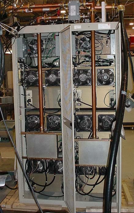
Click to zoom
Application Details
- Equipment Class
- TBC - Licensed Broadcast Station Transmitter
- Date of Grant
- Jul 26, 2007
- Application Purpose
- Original Equipment
- Date of Application
- Jun 17, 2007
- Equipment Note
- 3000-Watt UHF Digital Transmitter
- Frequency Range
- 614.00000000 - 806.00000000
- Company
- UBS-Axcera
- Country
- United States
Documents & Files
Document Text
Text extracted from the exhibit documents filed with the FCC. Open a document above to read the original.
Users Manual
Instruction Manual Innovator, LX Series Digital UHF Driver/Transmitter AXCERA, LLC 103 FREEDOM DRIVE, P.O. Box 525 LAWRENCE, PA 15055-0525 USA (724) 873-8100 • FAX (724) 873-8105 www.axcera.com • [email protected] Digital UHF Driver/Transmitter Table of Contents LX Series, Digital, Rev. 4 March 8, 2007 i TABLE OF CONTENTS CHAPTER 1 INTRODUCTION SECTION PAGE 1.1 Manual Overview...................................................................................1-1 1.2 Assembly Designation Numbers..............................................................1-1 1.3 Safety..................................................................................................1-2 1.4 Contact Information.........................................................................1-2 1.5 Material Return Procedure......................................................................1-2 1.6 Limited One Year Warranty for Axcera Products........................................1-3 CHAPTER 2 SYSTEM DESCRIPTION & REMOTE CONTROL CONNECTIONS 2.0 System Overview.................................................................................2-1 2.1 (Optional) Exciter Switcher Tray..............................................................2-2 2.2 Exciter Amplifier Chassis Assembly..........................................................2-3 2.2.1 DM8 Modulator Assembly..............................................................2-3 2.2.2 IF Processor Module.....................................................................2-4 2.2.3 VHF/UHF Upconverter Module........................................................2-6 2.2.4 Control & Monitoring/Power Supply Module.....................................2-7 2.2.5 Power Amplifier Module (In 5-50W Transmitters).............................2-8 2.2.6 Or Driver Amplifier Module (In High Power Transmitters)................2-10 2.3 RF Output Assemblies..........................................................................2-12 2.4 Control and Status...............................................................................2-12 2.4.1 Front Panel LCD Display Screen...................................................2-12 2.5 System Operation................................................................................2-12 2.5.1 Principles of Operation................................................................2-12 2.6 Maintenance.......................................................................................2-14 2.7 Customer Remote Connections.......................................................2-14 CHAPTER 3 SITE CONSIDERATIONS, INSTALLATION AND SETUP PROCEDURES 3.1 Site Considerations................................................................................3-1 3.2 Unpacking the Chassis w/Modules...........................................................3-5 3.3 Installing the Chassis w/Modules.............................................................3-5 3.4 AC Input...............................................................................................3-7 3.5 Setup and Operation..............................................................................3-8 3.5.1 Input Connections........................................................................3-8 3.5.2 Initial Turn On.............................................................................3-9 3.5.2.1 DM8 Digital Modulator Module LEDs on Front Panel.................3-9 3.5.2.2 IF Processor Module LEDs on Front Panel...............................3-9 3.5.2.3 VHF/UHF Upconverter Module LEDs on Front Panel.................3-9 3.5.2.4 Controller Module LEDs on Front Panel................................3-10 3.5.2.5 Power Amplifier or Driver Module LEDs on Front Panel..........3-10 3.5.3 Front Panel Screens for the Exciter/Amplifier Chassis Assembly.......3-10 3.5.4 Operational Procedure................................................................3-19 CHAPTER 4 CIRCUIT DESCRIPTIONS 4.0 (Optional) Exciter Switcher Tray..............................................................4-1 4.0.1 Exciter Switcher Control Board.......................................................4-1 4.1 DM8 Digital Modulator Module.................................................................4-1 4.1.1 Digital Modulator, DT1D Board.......................................................4-1 4.1.1.1 SMPTE-310 Input................................................................4-1 Digital UHF Driver/Transmitter Table of Contents LX Series, Digital, Rev. 4 March 8, 2007 ii TABLE OF CONTENTS - (Continued) SECTION PAGE 4.1.1.2 Channel Coder....................................................................4-1 4.1.1.3 Analog Output Section.........................................................4-2 4.1.1.4 Pilot Frequency Generation...................................................4-2 4.1.1.5 Voltage Requirements.........................................................4-2 4.1.2 VSB Front Panel Board..................................................................4-3 4.2 IF Processor Module...............................................................................4-3 4.2.1 IF Processor Board.......................................................................4-3 4.2.1.1 DM8 Modulator Selected......................................................4-3 4.2.1.2 External Modulated IF Selected.............................................4-3 4.2.1.3 Main IF Signal Path (Part 1 of 3)...........................................4-3 4.2.1.4 Input Level Detector Circuit..................................................4-4 4.2.1.5 Pin Diode Attenuator Circuit.................................................4-5 4.2.1.6 Main IF Signal Path (Part 2 of 3)...........................................4-5 4.2.1.7 Amplitude and Phase Pre Correction Circuits..........................4-6 4.2.1.8 Main IF Signal Path (Part 3 of 3)...........................................4-7 4.2.1.9 ALC Circuit......................................…
Text truncated - open the document above for the full version.
Users Manual
INSTRUCTION MANUAL Innovator LX Series Digital Power Amplifier Assembly AXCERA, LLC 103 FREEDOM DRIVE P.O. BOX 525 LAWRENCE, PA 15055-0525 USA (724) 873-8100 • FAX (724) 873-8105 www.axcera.com • [email protected] LX Series Digital Table of Contents Power Amplifier Assembly Volume 2, Rev. 1 June 15, 2006 i TABLE OF CONTENTS CHAPTER 1 INTRODUCTION SECTION PAGE 1.1 Manual Overview...................................................................................1-1 1.2 Assembly Designation Numbers..............................................................1-1 1.3 Safety..................................................................................................1-2 1.4 Contact Information.........................................................................1-2 1.5 Material Return Procedure......................................................................1-2 1.6 Limited One Year Warranty for Axcera Products........................................1-3 CHAPTER 2 AMPLIFIER ASSEMBLY DESCRIPTION, MAINTENANCE & REMOTE CONTROL CONNECTIONS 2.1 LX Series Power Amplifier Chassis Assembly Overview.............................2-1 2.1.1 Power Amplifier Chassis Configurations...........................................2-3 2.1.1.1 125 Watt Power Amplifier Chassis Configuration.....................2-3 2.1.1.2 250 Watt Power Amplifier Chassis Configuration.....................2-3 2.1.1.3 500W Power Amplifier Chassis Configuration..........................2-3 2.1.2 System Configurations..................................................................2-4 2.1.2.1 125W, 250W or 500W System Configurations........................2-4 2.1.2.2 1 kW System Configuration..................................................2-4 2.1.2.3 1.5 kW System Configuration...............................................2-4 2.1.2.4 2 kW System Configuration..................................................2-5 2.1.2.5 2.5 kW System Configuration...............................................2-5 2.1.2.6 3 kW System Configuration..................................................2-6 2.1.3 Power Amplifier Module Assembly, 250W........................................2-8 2.1.4 Power Supply Module Assembly...................................................2-10 2.1.5 Front Panel LCD Display Screens..................................................2-10 2.2 External Assembly...............................................................................2-10 2.2.1 Visual/Aural Metering Board........................................................2-10 2.3 System Operation................................................................................2-10 2.3.1 Principles of Operation................................................................2-11 2.4 Maintenance.......................................................................................2-12 2.5 Customer Remote Connections.......................................................2-12 CHAPTER 3 SITE CONSIDERATIONS, INSTALLATION AND SETUP PROCEDURES 3.1 Site Considerations................................................................................3-1 3.2 Unpacking the Chassis w/Modules and bandpass filter...............................3-5 3.3 Installing the Chassis w/Modules and filters..............................................3-5 3.4 AC Input...............................................................................................3-6 3.5 Setup and Operation..............................................................................3-7 3.5.1 Input Connections........................................................................3-7 3.5.2 Initial Turn On.............................................................................3-8 3.5.2.1 DM8 Digital Modulator Module LEDs on Front Panel.................3-8 3.5.2.2 IF Processor Module LEDs on Front Panel...............................3-8 3.5.2.3 VHF/UHF Upconverter Module LEDs on Front Panel.................3-8 3.5.2.4 Controller Module LEDs on Front Panel..................................3-9 3.5.2.5 Power or Driver Amplifier Module LEDs on Front Panel............3-9 3.5.3 Front Panel Screens for the Exciter/Amplifier Chassis Assembly.........3-9 3.5.4 Operation Procedure.....................................................................3-9 LX Series Digital Table of Contents Power Amplifier Assembly Volume 2, Rev. 1 June 15, 2006 ii TABLE OF CONTENTS - (Continued) SECTION PAGE CHAPTER 4 CIRCUIT DESCRIPTIONS Power Amplifier Chassis Assembly..........................................................4-1 4.1 Power Amplifier Module..........................................................................4-1 4.1.1 UHF Phase/Gain Board..................................................................4-1 4.1.2 150 Watt Driver Pallet Assembly....................................................4-2 4.1.3 150 Watt Driver, Dual Output Board...............................................4-2 4.1.4 UHF Module Assembly, RF Module Pallet, Philips..............................4-2 4.1.5 2 Way UHF Combiner Assembly.....................................................4-3 4.1.6 Amplifier Control Board.................................................................4-3 4.2 Power Supply Assembly.........................................................................4-5 4.3 External Assembly.................................................................................4-5 4.3.1 Dual Peak Detector Board.............................................................4-5 APPENDICES APPENDIX A INNOVATOR LX SERIES SPECIFICATIONS APPENDIX B DRAWINGS AND PARTS LISTS APPENDIX C TRANSMITTER LOG SHEET LX Series Digital Table of Contents Power Amplifier Assembly Volume 2, Rev. 1 iii LIST OF FIGURES FIGURE PAGE 1-1 Brady Marker Identification Drawing.................................................1-1 2-1 500W Digital Power Amplifier Assembly Racking Plan.........................2-3 3-1 1 kW Minimum Ventilation Configuration.........................…
Text truncated - open the document above for the full version.
External Photos
Axcera-LU3000ATD FCC Type Acceptance Report External Photos June 2007 2-1 2. EXTERNAL PHOTOS 2.1 Front view, complete LU3000ATD Transmitter with Optional Dual Exciters, Exciter Switcher (right), Axciter Modulator (w/Left Exciter) and DM8 Modulator Module (w/Right Exciter) Axcera-LU3000ATD FCC Type Acceptance Report External Photos June 2007 2-2 2.2 Rear view, complete Axcera-LU3000ATD Transmitter Axcera-LU3000ATD FCC Type Acceptance Report External Photos June 2007 2-3 2.3 Side View, Bandpass Filter Axcera-LU3000ATD FCC Type Acceptance Report External Photos June 2007 2-4 2.4 Front View, External Axciter Digital Modulator 2.5 Rear View, External Axciter Digital Modulator 2.6 Top View, External Axciter Digital Modulator
ID Label/Location Info
Axcera-LU3000ATD FCC Type Acceptance Report ID Label/Location Info June 2007 1-1 1. ID LABEL/LOCATION INFO 1.1 Rear Panel FCC Label 1.2 Rear Panel Manufacturer’s Label Axcera-LU3000ATD FCC Type Acceptance Report ID Label/Location Info June 2007 1-2 1.3 Front view, complete LU3000ATD Transmitter with Optional Dual Exciters, Exciter Switcher (right), Axciter Modulator (w/Left Exciter) and DM8 Modulator Module (w/Right Exciter) Axcera-LU3000ATD FCC Type Acceptance Report ID Label/Location Info June 2007 1-3 1.4 Rear view, complete Axcera-LU3000ATD Transmitter with FCC ID and Manufacturer’s Label
Internal Photos
Axcera-LU3000ATD FCC Type Acceptance Report Internal Photos June 2007 6-1 6. INTERNAL PHOTOS 6.1 Front view – Chassis Assembly (Exciter) 6.2 Side view – DM8 – Internal Digital Modulator Assembly (Exciter) Axcera-LU3000ATD FCC Type Acceptance Report Internal Photos June 2007 6-2 6.3 Side view - IF Processor Assembly – Used with DM8 Modulator (Exciter) 6.4 Side view – VHF/UHF Upconverter Assembly – Used with DM8 Modulator (Exciter) Axcera-LU3000ATD FCC Type Acceptance Report Internal Photos June 2007 6-3 6.5 Side view – Axciter Upconverter Assembly - Used with Axciter Modulator (Exciter) 6.6 Side view – Axciter Downconverter Assembly - Used with Axciter Modulator (Exciter) Axcera-LU3000ATD FCC Type Acceptance Report Internal Photos June 2007 6-4 6.7 Side view - Control / Power Supply Assembly (Exciter) 6.8 Side view - Power Amplifier Assembly (Exciter) Axcera-LU3000ATD FCC Type Acceptance Report Internal Photos June 2007 6-5 6.9 Front view – Chassis Assembly (External Power Amplifier) 6.10 Side view - Power Amplifier Assembly (External Power Amplifier) Axcera-LU3000ATD FCC Type Acceptance Report Internal Photos June 2007 6-6 6.11 Side view – Power Supply Assembly (External Power Amplifier) 6.12 Side view – 4-Way Combiner Assembly (External Power Amplifier) Axcera-LU3000ATD FCC Type Acceptance Report Internal Photos June 2007 6-7 6.13 Top view – External Axciter Digital Modulator
Operational Description
Axcera-LU3000ATD FCC Type Acceptance Report Operational Description June 2007 8-1 8. OPERATIONAL DESCRIPTION - MODEL Axcera-LU3000ATD 8.1 General Description The LU3000ATD is a complete 3000-watt UHF solid-state, digital transmitter. It operates at a nominal visual output power of 3000 watts average. 8.2 Technical Specifications Type of Emission .....................................................................6M00K1D Frequency Range.................... 470 MHz to 608 MHz & 614 MHz to 806 MHz Output Power........................................................3000 watts average 8.3 Performance Specifications Operating Frequency Range ..... 470 MHz to 608 MHz & 614 MHz to 806 MHz RF output - Nominal: Power ........................................................... 3000 watts average Impedance .................................................................... 50 ohms Connector .................................................................. 3-1/8” EIA Regulation of Output........................................................................ 3% Signal-to-Noise Ratio (SNR) ........................................... 27 dB or better Carrier Frequency Stability.......................................................±1000 Hz Out of Band: Compliant with FCC Mask (Measured in 30 KHz RBW, relative to total average power Channel Edge ± 500 KHz................................................ -47 dB or better 6 MHz Channel Edge .....................................................-110 dB or better Data Interface: Input Rate.................................................... 19.39 Mbps, 6 MHz Channel Input Interface..........................SMPTE 310M, Serial Differential ECL & TTL Electrical Requirements Power Line Voltage................................................... 230 volts, 50/60 Hz Power Consumption ............................................................20,500 watts Environmental Maximum Altitude ..................................................................8,500 feet Operational Temperature Range ...........................................0°C to +50°C Axcera-LU3000ATD FCC Type Acceptance Report Operational Description June 2007 8-2 Mechanical Dimensions: Width ..........................................................................44 inches Depth ..........................................................................34 inches Height..........................................................................74 inches Weight .......................................................................... 1330 lbs 8.4. System Overview The LU3000ATD is made up of the trays listed in Table 8-1. Table 8-1. LU3000ATD Major Trays and Assemblies MAJOR ASSEMBLY DESIGNATOR TRAY/ASSEMBLY NAME A1 UHF Exciter Assembly A2, A3, A4, A5, A6, A7 External Amplifier Assembly A8 Optional Axciter Modulator 8.4.1 Exciter Tray/External Amplifier Tray The output of the Exciter Tray (driver) drives the input to the External Amplifier Tray. 8.4.1.1 DM8 – Internal Digital Modulator Module (Exciter) The DM8 modulator is an ATSC compliant 8 VSB modulator that slides into the left most slot in the Innovator LX Driver chassis assembly. The DM8 modulator accepts a SMPTE- 310 MPEG data stream input and outputs a 6 MHz wide IF output centered at 44 MHz with a pilot carrier at 46.69 MHz. The DM8 modulator provides linear and nonlinear correction capability for the transmission path as well as internal test sources that are used during initial transmitter installation. All of the functions of the DM8 modulator are controlled from the LX Controller LCD display and pushbuttons. 8.4.1.2 Axciter – Enternal Digital Modulator Module (Exciter) The Axciter modulator is an ATSC compliant 8 VSB modulator that is used externally with the Innovator LX Driver chassis assembly. Like the DM8 modulator, the Axciter modulator also accepts a SMPTE-310 MPEG data stream input and outputs a 6 MHz wide IF output centered at 44 MHz. All of the functions of the Axciter modulator are controlled from the front panel pushbuttons. 8.4.1.3 IF Processor Module – Used with DM8 Only (Exciter) The IF Processor Assembly contains the IF Processor Board (1301977). The IF Processor provides pre-correction to ensure broadcast quality output signal. The pre-correction consists of amplitude linearity correction, Incidental Carrier Phase Modulation (ICPM) correction and frequency response correction. The IF Processor module is configured either for an analog or digital system. Pin 13C of the IF Processor module is grounded in analog systems and left not connected in digital systems. An IF Processor Interlock signal is used to report the presence of the IF Axcera-LU3000ATD FCC Type Acceptance Report Operational Description June 2007 8-3 Processor module to the Control Monitoring board. If the IF Processor interlock signal is not present, the transmitter/Exciter Driver RF output is Muted (turned off). If an analog IF Processor module is installed and the Modulation Present signal is not true, the transmitter / Exciter Driver output is Muted (turned off). The Control & Monitoring/Power Supply module uses the IF Processor module for System output power control. Through the front panel display or a remote interface, an operator can set the transmitter's RF output power. The range of RF power adjustment is between 0% (full off) and 105% (full power plus). A front panel IF Processor module potentiometer sets the upper limit of RF power at 120%. The system's Control Monitoring board compares the RF Power Monitoring module RF power level with the desired level and uses the IF Power Control PWM line to correct for errors. In digital systems, a digital level control (DLC) voltage is generated on the IF Processor module and sent to the digital modulator. RF power control is implemented by changing the DLC voltage provided to the digital modulator. The 'RF High' potentiometer sets the upper adjusted range of RF control circuit output to 120%. The IF Processor mod…
Text truncated - open the document above for the full version.
Parts List/Tune Up Info
Axcera-LU3000ATD FCC Type Acceptance Report Parts List/Tune-up Info June 2007 7-1 7. PARTS LIST/TUNE-UP INFO 7.1 Parts List The transmitter, can be subdivided as follows: Exciter Tray: DM8 – Internal Digital Modulator Module or External Axciter Digital Modulator Tray IF Processor Module (Used only with DM8 Modulator) VHF/UHF Upconverter Module (Used only with DM8 Modulator) or Axciter Upconverter (Used only with Axciter Modulator Tray) Axciter Downconverter (Used only with Axciter Modulator Tray) Control & Monitoring / Power Supply Module Power Amplifier Module External Amplifier Trays (Qty of 6): 4-Way Splitter (Qty of 6) Power Amplifier Module (Qty of 24) Power Supply Module (Qty of 12) 4-Way Combiner (Qty of 6) 7.2 Tune-up Information The LU3000ATD transmitter was aligned at the factory and should not require additional alignments to achieve normal operation. 7.2.1 Exciter Assembly This transmitter takes the IF from the digital modulator and converts the signal to the desired UHF On Channel RF Output at the systems output power level. 7.22 DM8 - Digital Modulator or Axciter Digital Modulator Note: Not present in Translator systems. The Digital Modulators have adjustments for modulation levels, and other related parameters. Verify that all red LEDs located on the IF Processor front panel are extinguished. The following details the meaning of each LED when illuminated: • DS1 (input fault) – Indicates that either abnormally low or no IF is present at the input of the module. • DS2 (ALC fault) – Indicates that the ALC circuit is unable to maintain the signal level requested by the ALC reference. This is normally due to excessive attenuation in the linearity signal path or the IF phase corrector signal path, or that switch SW1 is in the Manual ALC Gain position. • DS4 (Mute) – Indicates that a Mute command is present to the system. Switch the transmitter to Standby. The ALC is muted when the transmitter is in Standby. To monitor the ALC, preset R3, manual gain-adjust, on the front panel of the Upconverter Axcera-LU3000ATD FCC Type Acceptance Report Parts List/Tune-up Info June 2007 7-2 module, fully CCW. Move switch SW1, Auto/Man AGC, on the front panel of the Upconverter module, to the Manual position. Place the transmitter in Operate. Adjust the ALC GAIN pot on the front panel of the IF Processor to obtain +0.8 VDC on the LCD Display on the Controller/Power Supply in the ALC screen. Move the MAN/AUTO ALC switch back to Auto, which is the normal operating position. To adjust the AGC Cutback setting, raise the output power of the transmitter to 110%. Adjust R2, AGC Cutback, located on the front panel, CCW until the LED DS1, AGC Cutback, just starts to flash. Return the output power of the transmitter to 100%. 7.2.3 If Processor Module Assembly (Used with DM8 Only) On the LCD Display, located on the Controller/Power Supply Module, push the button to switch the transmitter to Operate. The setup of the RF output includes adjustments to the drive level of the Power Amplifier, the adjustment of the linearity and phase pre-distortion to compensate for any nonlinear response of the Power Amplifier on the front panel of the IF Processor module. Verify that all red LEDs located on the IF Processor front panel are extinguished. The following details the meaning of each LED when illuminated: • DS1 (input fault) – Indicates that either abnormally low or no IF is present at the input of the module. • DS2 (ALC fault) – Indicates that the ALC circuit is unable to maintain the signal level requested by the ALC reference. This is normally due to excessive attenuation in the linearity signal path or the IF phase corrector signal path, or that switch SW1 is in the Manual ALC Gain position. • DS4 (Mute) – Indicates that a Mute command is present to the system. Switch the transmitter to Standby. The ALC is muted when the transmitter is in Standby. To monitor the ALC, preset R3, manual gain-adjust, on the front panel of the Upconverter module, fully CCW. Move switch SW1, Auto/Man AGC, on the front panel of the Upconverter module, to the Manual position. Place the transmitter in Operate. Adjust the ALC GAIN pot on the front panel of the IF Processor to obtain +0.8 VDC on the LCD Display on the Controller/Power Supply in the ALC screen. Move the MAN/AUTO ALC switch back to Auto, which is the normal operating position. To adjust the AGC Cutback setting, raise the output power of the transmitter to 110%. Adjust R2, AGC Cutback, located on the front panel, CCW until the LED DS1, AGC Cutback, just starts to flash. Return the output power of the transmitter to 100%. 7.2.4 Linearity Correction Adjustment As shipped, the exciter was preset to include amplitude and phase pre-distortion. The pre- distortion was adjusted to approximately compensate the corresponding non-linear distortions of the Power Amplifier. NOTE: On the IF processor board inside the module the correction enable/disable jumper W12 on J30 must be in the Enable position, on pins 2 & 3. Set up a spectrum analyzer for 30 kHz resolution bandwidth and 30 kHz video bandwidth. Axcera-LU3000ATD FCC Type Acceptance Report Parts List/Tune-up Info June 2007 7-3 Connect the spectrum analyzer to monitor the intermodulation products of the RF output signal of the Power Amplifier. A typical digital spectrum is shown in Figure 5-1. There are three Linearity Corrector stage adjustments located on the front panel of the IF Processor Module. The adjustments are threshold settings that are adjusted as needed to correct for any amplitude or phase intermodulation problems. Adjust the top linearity correction adjustment R211 threshold cut in for the in phase amplitude distortion pre- correction that is needed. Next adjust the middle linearity correction adjustment R216 threshold cut in also for the in phase amplitude distortion pre-correction that is needed. Finally, adjust the bottom linearity correction adjustment R231 threshold cut in for the quadratu…
Text truncated - open the document above for the full version.
Schematics
5 5 4 4 3 3 2 2 1 1 DD CC BB AA Axcera REV ECO DATEAPV TITLE THIS PRINT IS THE PROPERTY OF AXCERA, IT SHALL NOT BE COPIED WITHOUT PERMISSION MATERIAL FINISH DWN CHK REL SCALESHEET REV REV E CO DATE A PV DWG. NO. --- ----- ----- 1303569B0 SCH., 2 WAY SPLITTER/PHASE SHIFTER, UHF (1303567) JKF 11/11/03 B1 OF 1 11/12/03TB 11/12/03TB CHGD CONN. OF U2 & U3. JKF B020111424 6/22/04TB J2 SMA 1 C2 .8-10pF U3 1084607 14 32 C4 .8-10pF J3 SMA 1 NOTE: 1) ALL RESISTORS ARE 1/8W UNLESS OTHERWISE NOTED. 2) ALL CAPACITORS ARE IN uF UNLESS OTHERWISE NOTED. 3) ALL INDUCTORS ARE IN uH UNLESS OTHERWISE NOTED. C1 .8-10pF U1 1084607 14 32 J1 SMA 1 R1 50 40W U2 1084607 14 32 C3 .8-10pF 9 9 8 8 7 7 6 6 5 5 4 4 3 3 2 2 1 1 EE DD CC BB AA Axcera REV ECO DATEAPV TITLE THIS PRINT IS THE PROPERTY OF AXCERA, IT SHALL NOT BE COPIED WITHOUT PERMISSION MATERIAL FINISH DWN CHK REL SCALESHEET REV REV E CO DATE A PV DWG. NO. --- ----- ----- 1159976C0 SCH., DUAL PEAK DETECTOR, SMT (1159965) PJK 2/23/00 B 1 OF 1 2/26/01 LRT2/26/01 LRT ANALOG DIGITAL B0 20092702 6 /11/01 UNCALIBRATED OUTPUT 1 O/P ANALOG (KEY) GND +12V -12V GND GND ANALOG OUTPUT 4 DIGITAL UNCAL. DIGITAL GND OUTPUT 3 GND ANALOG O/P OUTPUT 2 DIGITAL NOTE: TP1 & TP2 ARE PROVIDED FOR FUNCTION TEST PURPOSES ONLY, AND ARE ACCOMPLISHED BY ADDING VIA HOLE TO TOP OF PCB. REMOVED C 2, C4, L1, L2, CR3, AND C R4. R25 AND R 26 WERE 470K. R7 AND R8 WERE 2.2K. C7 A ND C8 WERE .0 01. ADDED J8, J9, W3, W4, R27-R 30. (PJK) LRT C0 20110722 3/4W 3/4W 3/4W 3/4W ADDED C2 & C4. J KF LRT 5 /16/03 W2 C16 300pF C4 .001 L6 .47 uH C12 300pF J6 1 2 3 R27 100K R24 100 R8 100K L10 .47 uH CR1 5082-2811 J7 1 2 3 R29 100K L5 .47 uH R19 1K C2 .001 R20 10K 1 2 3 J5 J9 1 2 3 R16 100 C8 .47 C11 300pF R15 100 R2 100 C10 300pF L4 .47 uH C7 .47 CR2 5082-2811 L7 .47 uH W3 C13 300pF L8 .47 uH C14 300pF R23 100 L9 .47 uH C3 100pF R1 100 1 2 3 J4 C15 300pF R4 100 R28 100K R17 100 R18 100 R26 2.2K J8 1 2 3 J1 J2 11 12 10 9 5 6 4 3 8 7 2 1 J3 - + U1C 8 9 10 + - U1D 12 13 14 C1 100pF R7 100K W1 1 2 3 CW R10 10K TP1 R25 2.2K TP2 1 2 3 CW R9 10K R3 100 W4 + - U1A 15906221 1 2 3 4 11 C5 0.1 uF + - U1B 5 6 7 R21 1K R30 100K R22 10K C6 0.1 uF L3 .47 uH C9 300pF
Schematics
55 44 33 22 11 D D C C B B A A Axcera REV ECO DATE APV TITLE THIS PRINT IS THE PROPE RTY OF AXCERA, IT SHALL NOT BE COPIED WITHOUT PERMISSION MATERIAL FINISH DWN CHKREL SCALE SHEET REV REV ECO DATEAPV DWG. NO. --- ---------- 1305940 B0 SCH., 8 VSB FRONT PANEL BD., LX (1305939) JKF 4/8/05 B1 OF 1 4/8/05 LAJ 4/8/05 LAJ POWER MPEGPLL APLL B RS-232 POWER MPEGPLL APLL BCOMKEY TX RX COM TX RX COM PLL B UNLOCKEDPLL A UNLOCKED MPEG NOT PRESENT KEY (NOT USED) (NOT USED) B0 20111868 ADDED R1, R2 & R3. ADDED"NOT USED" TO DS1 & J3. (CR) 11/15/05 LAJ J3 1234 GREEN RED DS4 R2 1K GREEN RED DS1 R3 1K GREEN RED DS2 R1150 J2 123456789 10 GREEN RED DS3 J1 123456789
Schematics
Axcera
Schematics
INSTRUCTION MANUAL Axciter Digital Modulator/Upconverter System AXCERA, LLC 103 FREEDOM DRIVE P.O. BOX 525 LAWRENCE, PA 15055-0525 USA (724) 873-8100 • FAX (724) 873-8105 www.axcera.com • [email protected] Digital ATSC Exciter-Modulator System Table of Contents Axcera Axciter, Rev. 0 i March 22, 2007 CHAPTER 1: INTRODUCTION......................................................................................................................1…
Text truncated - open the document above for the full version.
Contact Information
Applicant
David Hewitt(Engineering Manager)
Technical Contact
AxceraLance R. Trussa
[email protected]724-873-8100
103 Freedom Drive · Lawrence, Pennsylvania · United States
Non-Technical Contact
AxceraJames C. Mounts
[email protected]724-873-8100
Technical Specifications
| # | Rule Parts | Frequency Range | Power Output | Emission | Tolerance |
|---|---|---|---|---|---|
| 2 | 74 | 614 MHz - 806 MHz | 3000 W | 6M00K1D | 1000 Hz |
Other Applications from UBS-Axcera

OUSCU0TD-5-UBS
Mar 27, 2014200W UHF Digital Transmitter
Equipment Class
TBC - Licensed Broadcast Station Transmitter
OUSCL1TC-4
Sep 17, 2013400-Watt, 1.6 GHz DVB-H Transmitter
Equipment Class
TNB - Licensed Non-Broadcast Station Transmitter
OUSCLV2TD-4
Aug 22, 2013Low Band VHF Digital Broadcast Transmitter
Equipment Class
TBC - Licensed Broadcast Station Transmitter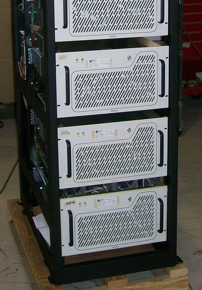
OUSCHV4TD
Jun 14, 20123000-Watt VHF Digital Transmitter
Equipment Class
TBC - Licensed Broadcast Station Transmitter
OUSCU0TD-5
Dec 14, 2011200 Watt UHF Digital Transmitter
Equipment Class
TBC - Licensed Broadcast Station Transmitter