OUSLU5000AT5000-Watt UHF Transmitter
UBS-Axcera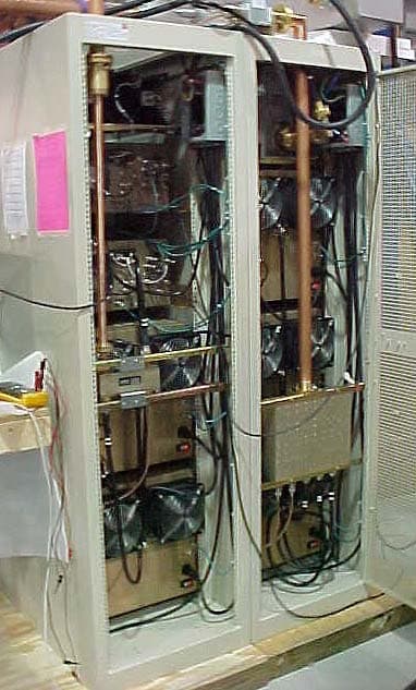
Click to zoom
Application Details
- Equipment Class
- TBC - Licensed Broadcast Station Transmitter
- Date of Grant
- Apr 26, 2005
- Application Purpose
- Original Equipment
- Date of Application
- Mar 15, 2005
- Equipment Note
- 5000-Watt UHF Transmitter
- Frequency Range
- 470.00000000 - 860.00000000
- Company
- UBS-Axcera
- Country
- United States
Documents & Files
Document Text
Text extracted from the exhibit documents filed with the FCC. Open a document above to read the original.
Users Manual
Instruction Manual Single Channel Exciter Switcher w/Innovator LX Series Transmitter Axcera, LLC 103 Freedom Drive, P.O. Box 525 Lawrence, PA 15055-0525 USA (724) 873-8100 • FAX (724) 873-8105 www.axcera.com • [email protected] Single Channel Exciter Switcher, LX Series (1305715) Table of Contents - Page 1 of 1 - 03/01/05 1. Introduction: 2. System: A. System Description B. Installation Instructions C. Initial Turn On Procedure D. System Operation Procedure E. Drawings: 1. Single Channel Exciter Switcher 500/1kW Interconnect........................1305746 2. Single Channel Exciter Switcher 5kW Interconnect..............................1305741 3. Single Channel Exciter Switcher Tray: A. Description B. Drawings: 1. Interconnect...............................................................................1305739 4. Subassemblies: This section contains the drawings of the boards and subassemblies that make up the Exciter Switcher. A drawing list of the Boards and Subassemblies as they appear in the section is located at the front of the section. 5. Maintenance: The Section contains information on the normal operation and maintenance of the Exciter Switcher. It also contains information on the plugs, jacks, sockets and pins that make up the cable assemblies in the Exciter Switcher. Single Channel Exciter Switcher, LX Series (1305715) System Description - Page 1 of 1 - The Single Channel Auto Switcher consists of (A1) a Single Channel Exciter Switcher Tray (1305715) with a separate (A2) coaxial transfer relay, mounted on a bracket that faces toward the rear of the cabinet, behind the Switcher Tray. The Exciter Switcher Tray is designed to monitor the selected On Air Exciter and automatically switch to the back up Exciter if the On Air Exciter should malfunction. The coaxial relay has the RF outputs from both Exciters connected to its inputs and, depending on if the energizing voltage is applied or not, the selected Exciter RF Output is connected to the external amplifiers and the RF output from the other exciter is connected to a load. Functionally the Single Channel Exciter Switcher Tray contains an Exciter Switcher Control Board (1305704), which provides the monitoring of the operation of both Exciters and the control of the automatic switching of the Exciters in case of malfunction in the On Air Exciter. ICs on the board monitor the operating parameters of the Exciters and determine if the Exciters are functioning properly. The front panel of the Exciter Switcher has an LCD display, which provides set up screens for the operation of the switching process. The coaxial relay has four “N” connectors that provide input and output connections to the relay. The RF Output from Exciter “A” connects to J21. The RF Output from Exciter “B” connects to J23. The Selected Exciter RF Output to the external amplifiers connects to J24. The Exciter “A/B” Load connects to J22, to which the RF output of the Off Air Exciter is connected. A wire harness connects to the relay from J14 on the Exciter Switcher Control Board. These connections provide the control voltages to the relay from the control board and status indication connections back to the control board. This Instruction Manual contains the Schematics, Interconnects, Assembly Drawings and Replacement Parts Lists needed for the troubleshooting of the Exciter Switcher. The Manual also contains information on the operation and maintenance of the Exciter Switcher. Single Channel Exciter Switcher, LX Series (1305715) Installation Procedure - Page 1 of 1 - NOTE: If the Single Channel Exciter Switcher is already installed as part of a Transmitter System then this section may be skipped. Remove the (A29) Exciter Switcher with the Exciter Switcher Board (A1), the Relay Panel (A2), all cables and the wire harness from the shipping box. Remove the packing material from around the Switcher and any accessories and inspect them for damage. Notify Axcera and the shipper if damage is found. The Exciter Switcher is designed to fit into a standard 19" rack normally between the two Exciters to be controlled. Mount the Assembly to the rack using the hardware found in the Installation Material Kit. Refer to the Single Channel Exciter Switcher Interconnect (1305739) and the system Interconnect (1305741 for 5 kW) while installing the wire harness and cabling to the proper Jacks and connectors. The following RF connections are made using RG-55 cables. Locate the cables labeled for the each of the following connections and physically make those connections. Labeling for the transmitter system is as follows: (A27) Exciter A, (A28) Exciter B, (A29) Exciter Switcher, (A30) Load, (A15) 2 Way Splitter then to (A5) on of the 4 Way Splitters, two are used in a 5kW system. (A2) Transfer Function Relay From\To (A27) Exciter A RF Input A29-J21 Exciter A RF Output A27-J25 (A30) Exciter A/B Load Output A29-J22 To Exciter A/B Load A30-J1 (A28) Exciter B RF Input A29-J23 Exciter B RF Output A28-J25 Selected Exciter RF Output A29-J24 To RF Splitter (A15) in 5kW Refer to the Single Channel Exciter Switcher Interconnect (1305739) and the system Interconnect (1305746 for 500/1 kW) while installing the wire harness and cabling to the proper Jacks and connectors. The following RF connections are made using RG-55 cables. Locate the cables labeled for the each of the following connections and physically make those connections. Labeling for the transmitter system is as follows: (A2) Exciter A, (A12) Exciter B, (A14) Exciter Switcher and (A15) Load. (A2) Transfer Function Relay From\To (A2) Exciter A RF Input A14-J21 Exciter A RF Output A2-J25 (A15) Exciter A/B Load Output A14-J22 To Exciter A/B Load A15-J1 (A12) Exciter B RF Input A14-J23 Exciter B RF Output A12-J25 Selected Exciter RF Output A14-J24 To the (A3) Power Amplifier Assembly The Exciter Switcher is ready for AC connection. Remove the AC Line Cord from the Installation Material Kit and install onto Jack J1 on the Exciter Switcher. Connect t…
Text truncated - open the document above for the full version.
Users Manual
%PDF-1.3%âãÏÓ 831 0 obj<< /Linearized 1 /O 833 /H [ 893 1588 ] /L 1743912 /E 12864 /N 121 /T 1727173 >> endobj xref831 23 0000000016 00000 n 0000000811 00000 n 0000002481 00000 n 0000002743 00000 n 0000003029 00000 n 0000004132 00000 n 0000004411 00000 n 0000005530 00000 n 0000005569 00000 n 0000006680 00000 n 0000006956 00000 n 0000006978 00000 n 0000007758 00000 n 0000007780 00000 n 0000008016 00000 n 0000009094 00000 n 0000009370 00000 n 0000009392 00000 n 0000010460 00000 n 0000010483 00000 n 0000012585 00000 n 0000000893 00000 n 0000002458 00000 n trailer<</Size 854/Info 804 0 R /Root 832 0 R /Prev 1727162 /ID[<9bcdbc73782a10633163890eee5fad51><9bcdbc73782a10633163890eee5fad51>]>>start xref0%%EOF 832 0 obj<< /Pages 805 0 R /Type /Catalog /StructTreeRoot 772 0 R >> endobj852 0 obj<< /S 2465 /C 2736 /Filter /FlateDecode /Length 853 0 R >> stream H‰ìVmlSU >çÜÛs»Ñ–{˽]7:·μÝmÁÁ c ` N (ƒÍñ1V ” ƒ•o л dcˆ 1Ä Ä¢& jL ~d_‰FMà Q ( Œ ̃hbb‚¾çžv ýã/oÚû>ç}Ÿ÷óœÛ[„ ŸƒÈ‚ ¾Ž 4|)HBV$"«Á×Qó6¿0è“#\ƒÃ' ta•úÂ...c+£è-— ßewiœ7Hk_Qø¹¤g ̄/a j/Ò"!`\Œ~•: -º5û ¬ƒäfû¥³ Õ åDÿ ] ÙçÊšÉÏK ?” •ïwæ\̾c9i©«:6æMyC2gÐ{Õ^h¹PùüwÝcw ́Û;%7–=©eáôó—μ›ÞwÞÝ7~škñi{üòùŽZë¼£½ 禖 ̧kíÓè!aFßžð¥ä¦XÅ ¼ 6 MμÿØ— DoŸhŠ...Žåα½d§ K«Ž÷ ïW–wæM¶éäwr¥ª#ö j>ÿ R_³ μõ·¿- >úíÌæ½ e§è B ̄V ½œZdÕO9?Íj!? ̄T=[x:¶( ̈¿çü šûÕ ý5=ÞH— ßìñ~’å,©éi-<âô4œ ̧-évù+At9= ¬îvz’ך º ž†·¼ÕÝÙžà‰3ý‡³Á½h°Ëã ö4 v” åã1Î’¼ ± #ÔS™¼ 6pÄ‘ ™™‹X ’¦ÒqDÐT,Qñ kª Qâª&RÉEUM ±Ïï’ ̈¦ŠØ_Xà{ ÈåÅ¢ªQI ®!¾( "ù-‰º ̄ áh^îx[¾Ç>‚à ̈œìÎ 2Ó M(æ@ K úÁ‰xBP, %P‚N ż 0«’F±8LO ̄ ¬W=Ç Qõ € ́ihÍ Á‚h¦ èX„ ̧<...ÍÎ`¦ Þ{1Ü1ôH3kAÕ hh1...\ I‰ @7 D(¹›a a Œð2u¬ ́‘ Ov8 Ô4Y H@·ÙÁ*©„ m _q·¿ÃL £4£ #ò²ö 0ÒR6¶€.âRI„‰a– ̧”ª’M³³òKY R>ZŽÙ4E ¶ ßø ß "ÜC“ö § Ø~xòKsÜTš 3óù S«Z€J£’3 ãöù Š hE÷äߣ Àp à(SÈY ÃŽf9œ£à„Ì* §! —qš )cO s ö ̃ªÓ€Í^& (-¶ `æ * ^¢Ó- ̄‹5®Y^Ѻ= b㪠+›ÖoX·zmóž–- › ›¶î®ßμmÇνÉí`mÝ· y#ð×T<¶pqõÜy•3§ïZÙ ́vçî=«WíزμeÓæĺæm Ö ‘ªù Ö< ~hƬ‡çÌ^ðÔÁ§ êW ˆ.Y ́ôÉeμ ’ŸÖö ́ QÛ &à% g¿@ì b½/ é +ŠÒ KìÎ 8c “› ¢ ^¦R2:¢ƒ.”f) Åê 0D îƤÉe¹ Vk ÆÍìñxœs o¦, # D¡È] ‹ â«äI± —%U”P Y³ * âò” Ìø–zV:' Ia)°3 «:ð ́š ØDB\ ̃wóÆz®D 0 ˆA¼Át¹PA]ºù ́Zñ •¢° ¦ O ?ë Yê ÒÓÃN=Áß Ì „† L ¡x¢sø2ã†B¡òH]}¼ó~Wzs‘ !ƒÿ•øÿï lÕ)”»® 2 ¾ æ-iÈ! Ê=Ž6¢ q‘lü‰ÄÒ$ ) { Er μ]–ÂvÅ/ –H...pËòKV›UQå>7.hO¡)èÐLQÆKUxâd¹ÍÑ{ -· ª† ×à ̈jÔâ tE7ÚD ÉÄ8‹á$M½ú ² )o[ üLÍ ¡ô¢B‡ñ U Ò6Q ̃Õò-2f A/ gKQ»OC ý`5–...1 :n—w|†D!åë·3÷vãë æ~”®fî-Bt¿é^R wkÒ-YÐ îèŠ F£/ADy³/ (D(+‹ëþ ` ä(æƒendstreamendobj853 0 obj1469 endobj833 0 obj<< /Type /Page /Parent 807 0 R /Resources << /Font << /F0 835 0 R /F1 837 0 R /F2 839 0 R /F3 845 0 R >> /XObject << /im1 850 0 R >> /ProcSet 851 0 R >> /Contents 838 0 R /MediaBox [ 0 0 612 792 ] /CropBox [ 0 0 612 792 ] /Rotate 0 >> endobj834 0 obj<< /Type /FontDescriptor /FontName /Verdana,Bold /Flags 16416 /FontBBox [ - 250 -210 2134 1005 ] /MissingWidth 544 /StemV 181 /StemH 181 /ItalicAngle 0 /CapHeight 1005 /XHeight 503 /Ascent 1005 /Descent -210 /Leading 215 /MaxWidth 1778 /AvgWidth 568 >> endobj835 0 obj<< /Type /Font /Subtype /TrueType /Name /F0 /BaseFont /TimesNewRoman /FirstChar 32 /LastChar 255 /Widths [ 250 333 408 500 500 833 778 180 333 333 500 564 250 333 250 278 500 500 500 500 500 500 500 500 500 500 278 278 564 564 564 444 921 722 667 667 722 611 556 722 722 333 389 722 611 889 722 722 556 722 667 556 611 722 722 944 722 722 611 333 278 333 469 500 333 444 500 444 500 444 333 500 500 278 278 500 278 778 500 500 500 500 333 389 278 500 500 722 500 500 444 480 200 480 541 778 500 778 333 500 444 1000 500 500 333 1000 556 333 889 778 611 778 778 333 333 444 444 350 500 1000 333 980 389 333 722 778 444 722 250 333 500 500 500 500 200 500 333 760 276 500 564 333 760 500 400 549 300 300 333 576 453 250 333 300 310 500 750 750 750 444 722 722 722 722 722 722 889 667 611 611 611 611 333 333 333 333 722 722 722 722 722 722 722 564 722 722 722 722 722 722 556 500 444 444 444 444 444 444 667 444 444 444 444 444 278 278 278 278 500 500 500 500 500 500 500 549 500 500 500 500 500 500 500 500 ] /Encoding /WinAnsiEncoding /FontDescriptor 836 0 R >> endobj836 0 obj<< /Type /FontDescriptor /FontName /TimesNewRoman /Flags 34 /FontBBox [ -250 -216 1158 1000 ] /MissingWidth 321 /StemV 73 /StemH 73 /ItalicAngle 0 /CapHeight 891 /XHeight 446 /Ascent 891 /Descent -216 /Leading 149 /MaxWidth 965 /AvgWidth 401 >> endobj837 0 obj<< /Type /Font /Subtype /TrueType /Name /F1 /BaseFont /Verdana,Bold /FirstChar 32 /LastChar 255 /Widths [ 342 402 587 867 711 1272 862 332 543 543 711 867 361 480 361 689 711 711 711 711 711 711 711 711 711 711 402 402 867 867 867 617 964 776 762 724 830 683 650 811 837 546 555 771 637 948 847 850 733 850 782 710 682 812 764 1128 764 737 692 543 689 543 867 711 711 668 699 588 699 664 422 699 712 342 403 671 342 1058 712 687 699 699 497 593 456 712 650 979 669 651 597 711 543 711 867 1000 711 1000 332 711 587 1049 711 711 711 1777 710 543 1135 1000 692 1000 1000 332 332 587 587 711 711 1000 711 964 593 543 1068 1000 597 737 342 402 711 711 711 711 543 711 711 964 598 850 867 480 964 711 587 867 598 598 711 721 711 361 711 598 598 850 1182 1182 1182 617 776 776 776 776 776 776 1094 724 683 683 683 683 546 546 546 546 830 847 850 850 850 850 850 867 850 812 812 812 812 737 735 713 668 668 668 668 668 668 1018 588 664 664 664 664 342 342 342 342 679 712 687 687 687 687 687 867 687 712 712 712 712 651 699 651 ] /Encoding /WinAnsiEncoding /FontDescriptor 834 0 R >> endobj838 0 obj[ 842 0 R 844 0 R ]endobj839 0 obj<< /Type /Font /Subtype /TrueType /Name /F2 /BaseFont /Verdana /FirstChar 32 /LastChar 255 /Widths [ 352 394 459 818 636 1076 727 269 454 454 636 818 364 454 364 454 636 636 636 636 636 636 636 636 636 636 454 454 818 818 818 545 1000 684 686 698 771 632 575 775 751 421 455 693 557 843 748 787 603 787 695 684 616 732 684 989 685 615 685 454 454 454 818 636 636 601 623 521 623 596 352 623 633 274 344 592 274 973 633 607 623 623 427 521 394 633 592 818 592 592 525 635 454 635 818 1000 636 1000 269 636 459 818 636 636 636 1521 684 454 1070 1000 685 1000 1000 269 269 459 459 545 636 1000 636 977 521 454 981 1…
Text truncated - open the document above for the full version.
Users Manual
INSTRUCTION MANUAL Innovator, LX Series UHF Analog Driver/Transmitter/Translator AXCERA, LLC 103 FREEDOM DRIVE P.O. BOX 525 LAWRENCE, PA 15055-0525 USA (724) 873-8100 • FAX (724) 873-8105 www.axcera.com • [email protected] UHF Analog Driver/Transmitter/Translator Table of Contents LX Series, Rev. 3 March 2, 2005 i TABLE OF CONTENTS CHAPTER 1 INTRODUCTION SECTION PAGE 1.1 Manual Overview............................................................................1-1 1.2 Assembly Designators......................................................................1-1 1.3 Safety...........................................................................................1-2 1.4 Contact Information.....................................................................1-2 1.5 Material Return Procedure.................................................................1-2 1.6 Limited One Year Warranty for Axcera Products.....................................1-3 CHAPTER 2 SYSTEM DESCRIPTION, MAINTENANCE & REMOTE CONTROL CONNECTIONS System Overview...........................................................................2-1 2.0 (Optional) Exciter Switcher Tray........................................................2-2 2.1 Exciter/Amplifier Chassis Assembly....................................................2-2 2.1.1 Receiver Module (not used in a transmitter system)......................2-2 2.1.2 Modulator Module (may not be used in a translator system)............2-4 2.1.3 IF Processor Module................................................................2-5 2.1.4 VHF/UHF Upconverter Module...................................................2-7 2.1.5 Control & Monitoring/Power Supply Module..................................2-9 2.1.6 Exciter PA Module used in 10-100W Xmitters. or Drvrs above 2kW..2-10 2.1.6.1 Driver Amplifier Module, used with 1kW or 2kW transmitters.2-12 2.1.7 RF Output Assemblies.............................................................2-14 2.2 Control and Status.........................................................................2-14 2.2.1 Front Panel LCD Display Screen................................................2-14 2.3 System Operation..........................................................................2-14 2.3.1 Principles of Operation............................................................2-14 2.4 Maintenance.................................................................................2-17 2.5 Customer Remote Connections...................................................2-17 CHAPTER 3 SITE CONSIDERATIONS, INSTALLATION AND SETUP PROCEDURES 3.1 Site Considerations..........................................................................3-1 3.2 Unpacking the Chassis w/Modules, bandpass and trap filters....................3-5 3.3 Installing the Chassis w/Modules and filters..........................................3-5 3.4 AC Input.......................................................................................3-6 3.5 Setup and Operation........................................................................3-7 3.5.1 Input Connections..................................................................3-7 3.5.2 Initial Turn On.......................................................................3-9 3.5.2.1 (Optional) Receiver Module LEDs on Front Panel...................3-9 3.5.2.2 Modulator Module LEDs on Front Panel...............................3-9 3.5.2.3 IF Processor Module LEDs on Front Panel...........................3-10 3.5.2.4 VHF/UHF Upconverter Module LEDs on Front Panel..............3-10 3.5.2.5 Controller Module LEDs on Front Panel..............................3-10 3.5.2.6 Power Amplifier or Driver Module LEDs on Front Panel..........3-10 3.5.3 Front Panel Screens for the (Optional) Exciter Switcher Assembly....3-10 3.5.4 Front Panel Screens for the Exciter/Amplifier Chassis Assembly......3-13 3.5.5 Operation Procedure..............................................................3-22 CHAPTER 4 CIRCUIT DESCRIPTIONS 4.0 (Optional) Exciter Switcher Tray (Used with dual exciter system)..............4-1 UHF Analog Driver/Transmitter/Translator Table of Contents LX Series, Rev. 3 March 2, 2005 ii TABLE OF CONTENTS - (Continued) SECTION PAGE 4.0.1 Exciter Switcher Control Board..................................................4-1 4.1 (Optional) Receiver Module (not used in a transmitter system).................4-1 4.1.1 IF ALC Board.........................................................................4-1 4.1.2 UHF Mixer/PLL Board...............................................................4-2 4.1.3 UHF Preamplifier Board............................................................4-2 4.2 Modulator Module (may not be used in a translator system)....................4-3 4.2.1 Analog Modulator Board...........................................................4-3 4.2.1.1 Mono, Balanced Audio Input.............................................4-3 4.2.1.2 Stereo, Composite Audio Input.........................................4-3 4.2.1.3 SAP/PRO, Subcarrier Audio Input......................................4-3 4.2.1.4 Audio Modulation of the 3.4 MHz VCO ................................4-4 4.2.1.5 Phase Lock Loop (PLL) Circuit...........................................4-4 4.2.1.6 Main Video Signal Path (Part 1 of 2)...................................4-5 4.2.1.7 Delay Equalizer Circuits...................................................4-5 4.2.1.8 Sync Tip Clamp Circuit....................................................4-5 4.2.1.9 Main Video Signal Path (Part 2 of 2)...................................4-6 4.2.1.10 45.75 MHz Oven Oscillator Circuit....................................4-6 4.2.1.11 Visual Modulator Circuit.................................................4-7 4.2.1.12 Aural Modulator Circuit..................................................4-7 4.2.1.13 Combining the 45.75 MHz & 41.25 MHz IF Signals..............4-7 4.2.1.14 Voltage Requirements...............…
Text truncated - open the document above for the full version.
Users Manual
INSTRUCTION MANUAL Innovator LX Series Power Amplifier Assembly AXCERA, LLC 103 FREEDOM DRIVE P.O. BOX 525 LAWRENCE, PA 15055-0525 USA (724) 873-8100 • FAX (724) 873-8105 www.axcera.com • [email protected] LX Series Power Amplifier Assembly Table of Contents LX Series, Rev. 0 November 25, 2003 i TABLE OF CONTENTS CHAPTER 1 INTRODUCTION SECTION PAGE 1.1 Manual Overview............................................................................1-1 1.2 Assembly Designation Numbers.........................................................1-1 1.3 Safety..........................................................................................1-1 1.4 Maintenance..................................................................................1-2 1.5 Material Return Procedure................................................................1-2 1.6 Limited One-Year Warranty for Axcera Products....................................1-3 CHAPTER 2 SYSTEM DESCRIPTION & REMOTE CONTROL CONNECTIONS 2.1 LX Series Power Amplifier Assembly Overview.....................................2-1 2.1.1 Power Amplifier Module, 250 Watt.............................................2-1 2.1.2 Power Supply Module Assembly.................................................2-3 2.1.3 Front Panel LCD Display Screens...............................................2-3 2.2 System Operation...........................................................................2-3 2.2.1 Principles of Operation.............................................................2-4 2.3 Customer Remote Connections.....................................................2-5 CHAPTER 3 SITE CONSIDERATIONS, INSTALLATION AND SETUP PROCEDURES 3.1 Site Considerations.........................................................................3-1 3.2 Unpacking the Chassis w/Modules, bandpass and trap filters....................3-4 3.3 Installing the Chassis w/Modules and filters..........................................3-4 3.4 AC Input.......................................................................................3-5 3.5 Setup and Operation.......................................................................3-5 3.5.1 Input Connections..................................................................3-5 3.5.2 Front Panel Screens for the Exciter/Amplifier Chassis Assembly.......3-7 3.5.3 Initial Turn On......................................................................3-14 CHAPTER 4 CIRCUIT DESCRIPTIONS 4.1 Power Amplifier Module....................................................................4-1 4.1.1 UHF Phase/Gain Board............................................................4-1 4.1.2 150 Watt Driver Pallet Assembly................................................4-1 4.1.3 150 Watt Driver, Dual Output Board...........................................4-1 4.1.4 UHF Module Assembly, RF Module Pallet, Philips...........................4-2 4.1.5 2 Way UHF Combiner Assembly.................................................4-2 4.1.6 Amplifier Control Board...........................................................4-3 4.2 Power Supply Assembly...................................................................4-5 CHAPTER 5 DETAILED ALIGNMENT PROCEDURES 5.1 Module Replacement.......................................................................5-1 5.1.1 Initial Test Setup....................................................................5-1 5.2 Innovator LX Series Exciter/Amplifier Chassis Assembly..........................5-2 5.2.1 Linearity Correction Adjustment................................................5-3 5.2.2 Frequency Response Delay Equalization Adjustment......................5-4 5.2.3 Calibration of Forward Output Power Level..................................5-4 5.2.4 Calibration of Reflected Output Power Level.................................5-5 5.3 Bandpass Filter Assembly.................................................................5-5 LX Series Power Amplifier Assembly Table of Contents LX Series, Rev. 0 November 25, 2003 ii TABLE OF CONTENTS - (Continued) 5.4 UHF Trap Filter Assembly..................................................................5-5 5.4.1 The Effects of Tuning the Output Trap Filter.................................5-6 APPENDICES APPENDIX A INNOVATOR LX SERIES SPECIFICATIONS APPENDIX B DRAWINGS AND PARTS LISTS LX Series Power Amplifier Assembly Table of Contents LX Series, Rev. 0 iii LIST OF FIGURES FIGURE PAGE 3-1 1 kW Minimum Ventilation Configuration.......................................3-4 3-2 Front and Rear View Reconnection Drawing...................................3-5 3-3 Rear View of LX Series Transmitter..............................................3-6 4-1 UHF Amplifier Module, 250 Watts.................................................4-2 5-1 Typical Red Field Spectrum........................................................5-4 LX Series Power Amplifier Assembly Table of Contents LX Series, Rev. 0 iv LIST OF TABLES TABLE PAGE 2-1 LX Series Power Amplifier Assemblies...........................................2-1 2-2 Power Amplifier Status Indicators................................................2-3 2-3 Power Amplifier Control Adjustments............................................2-3 2-4 Power Amplifier Sample.............................................................2-3 2-5 Pioneer Chassis Customer Remote Connections.......................2-5 3-1 Rear Chassis Connections for LX Series Transmitter........................3-6 3-2 Menu 01 Splash Screen #1........................................................3-7 3-3 Menu 02 Splash Screen #2........................................................3-7 3-4 Menu 10 Main Screen................................................................3-7 3-5 Menu 11 Error List Access Screen................................................3-8 3-6 Menu 12 Transmitter Device Data Access Screen............................3-8 3-7 Menu 13 Transmitter Configuration Access Screen...................…
Text truncated - open the document above for the full version.
External Photos
Axcera-LU5000AT FCC Type Acceptance Report External Photos February 2005 2-1 2. EXTERNAL PHOTOS 2.1 Front view, complete LU5000AT Transmitter Axcera-LU5000AT FCC Type Acceptance Report External Photos February 2005 2-2 2.2 Rear view, complete Axcera-LU5000AT Transmitter Axcera-LU5000AT FCC Type Acceptance Report External Photos February 2005 2-3 2.3 Rear view, Axcera-LU5000AT Transmitter (Cabinet Combiner) 2.4 Side view, Axcera-LU5000AT Transmitter (Band-pass Filter-right and Trap Filter-left)
ID Label/Location Info
Axcera-LU5000AT FCC Type Acceptance Report ID Label/Location Info February 2005 1-1 1. ID LABEL/LOCATION INFO 1.1 Rear Panel FCC Label 1.2 Rear Panel Manufacturer’s Label Axcera-LU5000AT FCC Type Acceptance Report ID Label/Location Info February 2005 1-2 1.3 Rear view, complete Axcera-LU5000AT Transmitter with FCC label 1.4 Axcera-LU5000AT FCC Type Acceptance Report ID Label/Location Info February 2005 1-3 1.4 Rear view, Axcera-LU5000AT Transmitter with FCC Label (close-up). 1.5 Rear view, Axcera-LU5000AT Transmitter with Manufacturer’s label (close-up)
Internal Photos
Axcera-LU5000AT FCC Type Acceptance Report Internal Photos February 2005 6-1 6. INTERNAL PHOTOS 6.1 Front view – Chassis Assembly (Exciter) 6.2 Side view - Modulator Assembly (Exciter) Axcera-LU5000AT FCC Type Acceptance Report Internal Photos February 2005 6-2 6.3 Side view - IF Processor Assembly (Exciter) 6.4 Side view – VHF/UHF Upconverter Assembly (Exciter) Axcera-LU5000AT FCC Type Acceptance Report Internal Photos February 2005 6-3 6.5 Side view - Control / Power Supply Assembly (Exciter) 6.6 Side view - Power Amplifier Assembly (Exciter) Axcera-LU5000AT FCC Type Acceptance Report Internal Photos February 2005 6-4 6.7 Front view – Chassis Assembly (External Power Amplifier) 6.8 Side view - Power Amplifier Assembly (External Power Amplifier) Axcera-LU5000AT FCC Type Acceptance Report Internal Photos February 2005 6-5 6.9 Top view – Power Supply Assembly (External Power Amplifier) 6.10 Side view – 4-Way Combiner Assembly (External Power Amplifier) Axcera-LU5000AT FCC Type Acceptance Report Internal Photos February 2005 6-6 6.11 Top view – Exciter Switcher Assembly (optional)
Operational Description
Axcera-LU5000AT FCC Type Acceptance Report Operational Description February 2005 8-1 8. OPERATIONAL DESCRIPTION - MODEL Axcera-LU5000AT 8.1 General Description The LU5000AT is a complete 5000-watt UHF solid-state, internally diplexed television transmitter. It operates at a nominal visual output power of 5000 watts peak sync and an average aural output power of 500 watts, at an A/V ratio of 10 dB, 10% sound. 8.2 Technical Specifications Type of Emissions: Visual .......................................................................... 5M75C3F Aural ............................................................................250KF3E Frequency Range....................... 470 MHz to 860 MHz (any 6-MHz channel) Output Power Visual .........................................................5000 watts peak sync Aural .............................................................. 500 watts average Maximum Power Rating Visual ....................................................... 5000 watts peak visual Aural ...................................................... 500 watts average aural Power Consumption ............................................................16,700 watts 8.3 Performance Specifications Visual Performance Operating Frequency Range ...................................... 470 MHz to 860 MHz RF output - Nominal: Power .........................................................5000 watts peak sync Impedance .................................................................... 50 ohms Connector.................................................................. 3 1/8” EIA Visual Sideband Response: -1.25 MHz and below ........................................................... -20B -0.75 to -0.5 MHz..................................................... +0.5, -2.0dB -0.5 MHz to +3.58 MHz....................................................±0.5 dB 3.58 MHz to 4.18 MHz.............................................. +0.5, -1.0 dB Variation of Frequency Response with Brightness...........................±0.5 dB Differential Phase ............................................................................ ±3° Incidental Phase Modulation.............................................................. ±3° Differential Gain .............................................................................. 5% Low Frequency Linearity ................................................................... 5% Intermodulation Products .............................................. -52 dB (red field) Output Variation (Over 1 Frame) ....................................................... 2% Regulation of Output........................................................................ 3% Axcera-LU5000AT FCC Type Acceptance Report Operational Description February 2005 8-2 Signal-to-Noise Ratio ................................................................. 55 dB 2t K-Factor.................................................................................. 2% Harmonic Radiation .....................................................................-60 dB Spurious (>3 MHz from channel edge) ...........................................-50 dB Carrier Frequency Stability....................................................... ±1000 Hz Aural Performance Frequency Deviation Capability (Transmitters) ............................. ±75 kHz Distortion .....................................................................................0.5% FM Noise ....................................................................................-60 dB AM Noise ....................................................................................-55 dB Visual to Aural Separation ......................................... 4.5 MHz, ±100 Hz Composite Audio Input (Multi-channel sound - Transmitters) Input Level ..................................…
Text truncated - open the document above for the full version.
Contact Information
Applicant
David Hewitt(Engineering Manager)
Technical Contact
AxceraLance R Trussa
[email protected]724-873-8100
103 Freedom Drive · Lawrence, Pennsylvania · United States
Non-Technical Contact
AxceraJames C Mounts
[email protected]724-873-8100
Technical Specifications
| # | Rule Parts | Frequency Range | Power Output | Emission | Tolerance |
|---|---|---|---|---|---|
| 2 | 74 | 470 MHz - 860 MHz | 5000 W | 5M75C3F | 1000 Hz |
Other Applications from UBS-Axcera

OUSCU0TD-5-UBS
Mar 27, 2014200W UHF Digital Transmitter
Equipment Class
TBC - Licensed Broadcast Station Transmitter
OUSCL1TC-4
Sep 17, 2013400-Watt, 1.6 GHz DVB-H Transmitter
Equipment Class
TNB - Licensed Non-Broadcast Station Transmitter
OUSCLV2TD-4
Aug 22, 2013Low Band VHF Digital Broadcast Transmitter
Equipment Class
TBC - Licensed Broadcast Station Transmitter
OUSCHV4TD
Jun 14, 20123000-Watt VHF Digital Transmitter
Equipment Class
TBC - Licensed Broadcast Station Transmitter
OUSCU0TD-5
Dec 14, 2011200 Watt UHF Digital Transmitter
Equipment Class
TBC - Licensed Broadcast Station Transmitter